EP1003290A2 - Elektronische Vorrichtung und Verfahren zur Unterspannungserkennung - Google Patents
Elektronische Vorrichtung und Verfahren zur Unterspannungserkennung Download PDFInfo
- Publication number
- EP1003290A2 EP1003290A2 EP99309279A EP99309279A EP1003290A2 EP 1003290 A2 EP1003290 A2 EP 1003290A2 EP 99309279 A EP99309279 A EP 99309279A EP 99309279 A EP99309279 A EP 99309279A EP 1003290 A2 EP1003290 A2 EP 1003290A2
- Authority
- EP
- European Patent Office
- Prior art keywords
- voltage
- low
- electronic device
- data
- voltage detection
- Prior art date
- Legal status (The legal status is an assumption and is not a legal conclusion. Google has not performed a legal analysis and makes no representation as to the accuracy of the status listed.)
- Withdrawn
Links
Images


Classifications
-
- G—PHYSICS
- G06—COMPUTING OR CALCULATING; COUNTING
- G06F—ELECTRIC DIGITAL DATA PROCESSING
- G06F1/00—Details not covered by groups G06F3/00 - G06F13/00 and G06F21/00
- G06F1/26—Power supply means, e.g. regulation thereof
- G06F1/28—Supervision thereof, e.g. detecting power-supply failure by out of limits supervision
-
- G—PHYSICS
- G06—COMPUTING OR CALCULATING; COUNTING
- G06F—ELECTRIC DIGITAL DATA PROCESSING
- G06F11/00—Error detection; Error correction; Monitoring
- G06F11/07—Responding to the occurrence of a fault, e.g. fault tolerance
- G06F11/0703—Error or fault processing not based on redundancy, i.e. by taking additional measures to deal with the error or fault not making use of redundancy in operation, in hardware, or in data representation
- G06F11/0751—Error or fault detection not based on redundancy
-
- G—PHYSICS
- G01—MEASURING; TESTING
- G01R—MEASURING ELECTRIC VARIABLES; MEASURING MAGNETIC VARIABLES
- G01R19/00—Arrangements for measuring currents or voltages or for indicating presence or sign thereof
- G01R19/165—Indicating that current or voltage is either above or below a predetermined value or within or outside a predetermined range of values
- G01R19/16533—Indicating that current or voltage is either above or below a predetermined value or within or outside a predetermined range of values characterised by the application
- G01R19/16538—Indicating that current or voltage is either above or below a predetermined value or within or outside a predetermined range of values characterised by the application in AC or DC supplies
- G01R19/16542—Indicating that current or voltage is either above or below a predetermined value or within or outside a predetermined range of values characterised by the application in AC or DC supplies for batteries
Definitions
- the present invention relates to electronic devices, for example, though not exclusively, devices equipped with electronic circuits that are driven by power supply means such as a battery, and a low-voltage detection method for detecting low voltage.
- Portable electronic devices are well known. Many of these portable electronic devices are battery driven and driven by a primary or secondary battery. Some examples of these kinds of electronic devices are, portable game devices, portable audio devices and cellular telephones.
- Fig. 1 is a block diagram showing the configuration of a previously proposed low-voltage detection circuit. As shown in Fig. 1, the low-voltage detection circuit 101 is equipped with a BGR circuit 102 and a comparator 103.
- the BGR circuit 102 is a constant-voltage output circuit called the "Band Gap Reference.”
- the BGR circuit 102 outputs a predetermined absolute reference voltage Vref.
- the comparator 103 compares the reference voltage Vref and the actual power-supply voltage Vlevel, and when the power-supply voltage Vlevel drops below the reference voltage Vref, it outputs a low-voltage detection signal Vdd_Low.
- the system uses this Vdd_Low signal as a trigger to perform necessary processing such as displaying "Battery End" or to save data for the application being executed.
- the reference voltage Vref is generally determined to correspond to the lowest operable voltage for the internal circuits, however, the actual lowest operable voltage of the elements of the internal circuits, such as the semiconductors or the like, may vary depending on the manufacturing process or operating conditions. Therefore, depending on the variation of elements and operating conditions, "Batter End” was sometimes displayed for batteries that could still be used.
- Embodiments of the present invention can provide an electronic device and low-voltage detection method which makes it possible to use battery capacity effectively.
- the electronic device comprises an electronic circuit which is driven by a drive voltage supplied from a power-supply unit, a memory unit which is driven by the drive voltage, a comparison unit which writes data to the memory unit, after which it reads the data that have been written and compares the written data with the read data, and a judgment unit which judges whether or not the electronic circuit is operating properly based on the comparison results of the comparison unit.
- the low-voltage detection method is a low-voltage detection method which monitors the drive voltage that is supplied to an electronic circuit of an electronic device, and which comprises a comparison step wherein data are written to the memory unit that is driven by the drive voltage, after which the data that have been written are read and the written data are then compared with the read data, and a judgment step wherein the value of the drive voltage is judged based on the comparison results as to whether or not it has dropped below the minimum operable voltage value for the electronic circuit.
- a second electronic device comprises a memory that is driven by voltage supplied from a battery, and a CPU that is driven by the voltage.
- the CPU performs a write test for the memory, and based on the results of this write test, judges whether or not the voltage has dropped below the minimum operable voltage.
- a second low-voltage detection method is a low-voltage detection method which monitors the voltage supplied to the electronic device, and it comprises a step that performs a write test for the memory that is driven by the voltage, and a judgment step that judges, based on the results of the write test, whether or not the voltage has dropped below the minimum operable voltage.
- Figure 1 is a block diagram which shows the configuration of a conventional low-voltage detection circuit that performs low-voltage detection.
- Figure 2 is a block diagram which shows the configuration of an electronic device for which the present invention is applied.
- Figure 3 is a flowchart which shows the flow of processes for detecting the minimum operable voltage by data matching test of the flash memory.
- Figure 4 is a block diagram which shows the configuration of another electronic device for which the present invention is applied.
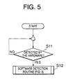
- Figure 5 is a flowchart which shows the flow of the process for detecting the low voltage together with the low-voltage detection circuit 6.
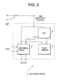
- Fig. 2 is a block diagram which shows the configuration of an electronic device for which the present invention is applied.
- the electronic device 1 comprises a peripheral circuit 2, battery 3, flash memory 4 and CPU 5.
- This electronic device 1 functions, for example, as a portable game device.
- the electronic device 1 is constructed as a single-voltage drive system wherein the peripheral circuit 2, flash memory 4 and CPU 5 are driven by one battery 3.
- the flash memory 4 and CPU 5 form a low-voltage detection system which monitors the value of the voltage output from the battery 3.
- the peripheral circuit 2 is an electronic circuit such as an interface circuit which performs signal input or output between external devices.
- the peripheral circuit 2 is driven by the battery 3.
- the minimum operable voltage of the peripheral circuit 2, is 2.0 V in this embodiment.
- the minimum operable voltage is the minimum voltage required for operating the electronic circuits.
- the battery 3 is the power-supply means which supplies drive voltage to each of the parts of the electronic device 1.
- the battery 3 can be, for example, a primary battery or secondary battery.
- the output voltage of the battery 3 is 3.0 V.
- the flash memory 4 is driven by the battery 3 and is the storage means to which the CPU 5 writes data or reads data from.
- the flash memory 4 is a non-volatile memory.
- the minimum operable voltage for the flash memory 4 is 2.4 V.
- the CPU 5 is a central processing unit which controls the entire system.
- the minimum operable voltage for the CPU 5 is 1.8 V.
- the standard voltage of the battery 3 is 3.0 V, and the voltage drops according to the power consumption of the system.
- the minimum operable voltage differs a little for each block and is; 1,8 V for the CPU 5, 2.0 V for the peripheral circuit 2 and 2.4 V for the flash memory.
- the reason that the minimum operable voltage for each block is different is that the components of each block, operating speed, circuit configuration and the like for each block are different.
- the minimum operable voltage of the flash memory 4 is larger than that of the other electronic circuits, namely the minimum operable voltage of the peripheral circuit 2 and the CPU 5.
- the flash memory 4 requires a lot of power for writing (programming) data, so the minimum operable voltage is large.
- This embodiment uses the fact the minimum operable voltage which enables writing to the flash memory 4 is the strictest condition, and performs a write test of the flash memory 4, and based on the results of the write test, it judges whether or not the voltage output from the battery 3 has dropped below the minimum operable voltage of the electronic device 1.
- the CPU 5 has a comparison function, whereby after data has been written to the flash memory 4, the data that has been written is read and the read data is compared with the written data, and it has a judgment function that, based on the comparison results, determines whether or not operation is proper.
- these functions are implemented by having the CPU 5 execute certain software (program).
- the CPU 5, by employing the comparison function, performs a matching test of the data that are written to and read from the flash memory 4. For example, the CPU 5 writes predetermined data to a predetermined area of the flash memory 4 and reads data from that area and performs a matching test of that data.
- the CPU 5 determines whether or not the electronic device 1 can operate properly. In other words, based on the results of the data matching test, the CPU 5 determines whether or not the voltage output from the battery 3 has dropped below the minimum operable voltage for the electronic device 1. If the data do not match, then the CPU determines that the voltage output from the battery 3 has dropped below the reference minimum operable voltage of the flash memory 4, or in the case of this embodiment, below 2.4 V.
- the CPU 5 performs data matching at a set interval (for example, 1 to 10 minute interval), and detects that the voltage output from the battery 3 has dropped below the minimum operable voltage.
- a set interval for example, 1 to 10 minute interval
- the CPU 5 periodically writes predetermined data to a predetermined area of the flash memory 4 and then immediately reads data from that area and performs a matching test to determine whether or not the voltage output from the battery 3 has dropped below the real minimum operable voltage of an actual element under the operating conditions at that time.
- the frequency of the test, the amount of data and the memory array area are selected according to the desired product performance for the system and the physical characteristics of the memory.
- the CPU 5 knows which areas in the flash memory 4 are not being used, it can select and use an arbitrary address from among the unused areas.
- a predetermined data pattern can be used as the pattern for the data to be written.
- the CPU 5 is given a random number generator function, then data according to the random number generated by that random number generator function can be used.
- the CPU 5 determines that the voltage output from the battery 3 has dropped below the minimum operable voltage, it performs necessary processes such as saving data or displaying "Battery End.”
- each of the blocks of the electronic device 1 is implemented individually on the motherboard, or for all or part of them to be integrated onto the same LSI.
- Fig. 3 is a flowchart that shows the flow of processes that occur in the matching test of the flash memory 4. These processes can be divided into generation of the test cycle (step S1 to step S2), matching test by writing data to and reading data from the flash memory 4 (step S3 to step S5) and battery end processing (step 6).
- step S1 the CPU 5 starts the timer provided in the electronic device 1. With this timer, the CPU 5 performs the operations from step S2 with the periodic test timing.
- step S2 the CPU 5 judges whether or not the current time corresponds to test cycle. That is, the CPU 5 judges whether or not it is the timing to perform the matching test of the data in the flash memory 4. This judgment may be performed based on the count value of the timer, or can be performed by using an interrupt from the timer. In step S2, if it is determined that it is the test timing, the CPU 5 advances to step S3.
- step S3 the CPU 5 writes predetermined data to a predetermined address in the flash memory 4, then continuing in step S4, the CPU 5 reads the data from the same address.
- step S5 the CPU 5 judges whether or not the read data is equal to the data that had been written. If the CPU 5 determines that the data match, then it returns to step S2. On the other hand, if it was determined that the data did not match, it advances to step S6. Before advancing to step S6, it is also possible to perform the multiple write tests using other data.
- step S6 the CPU 5 performs necessary processing such as saving data or displaying "Battery End.”
- the electronic device 1 determines whether or not the voltage output from the battery 3 has dropped below the minimum operable voltage.
- the electronic device 1 detects the actual minimum operable voltage. By doing so, the electronic device 1 can continue operating, depending on variations in element and operating conditions, until the voltage reaches the actual minimum operable voltage, and thus it is possible to effectively use the electric charge amount of the battery.
- the voltage of the power supply is monitored by a low-voltage detection circuit, and when the voltages drops to where it is near the minimum operable voltage, the power-supply voltage will then be monitored by the software.
- Fig. 4 is a block diagram which shows the construction of a second electronic device la to which the present invention has been applied.
- the electronic device la is constructed such that a low-voltage detection circuit 6 is added to the electronic device shown in Fig. 2.
- the electronic device la is constructed as a single-voltage drive system wherein the peripheral circuit 2, flash memory 4, CPU 5 and low-voltage detection circuit 6 are driven by one battery 3.
- the flash memory 4, CPU 5 and low-voltage detection circuit 6 form a low-voltage detection system which monitors the value of the voltage output from the battery 3.
- the low-voltage detection circuit 6 is a low-voltage detection means that monitors the voltage output from the battery 3.
- the low-voltage detection circuit 6 is the same as the low-voltage detection circuit 101 shown in Fig. 1. That is, the low-voltage detection circuit 6 comprises a BGR circuit 102 and comparator 103.
- the reference voltage Vref that is output from the BGR circuit 102 is compared with the actual power-supply voltage Vlevel by the comparator 103, and it detects when the voltage of the battery 3 drops to a predetermined voltage.
- the low-voltage detection circuit 6 outputs a detection trigger signal to the CPU 5 when the voltage output from the battery 3 reaches the predetermined voltage.
- the low-voltage detection circuit 6 outputs a detection trigger signal when the output voltage drops to a value near the minimum operable voltage of 2.4 V of the flash memory 4 (for example, 2.5 V).
- the CPU 5 detects the detection trigger signal from the low-voltage detection circuit 6, it switches over to the function for software monitoring of the minimum operable voltage. After software monitoring has begun, operation of the low-voltage detection circuit may be stopped.
- the CPU 5 monitors the voltage output from the battery 3 using hardware, namely the low-voltage detection circuit 6, until the voltage reaches a predetermined voltage, then after the voltage has reached that value, the CPU 5 judges the minimum operable voltage with software in the same manner as was done in the first embodiment.
- the CPU 5 switches from hardware monitoring to software monitoring when the voltage output from the battery 3 is near to the minimum operable voltage of 2.4 V of the flash memory 4.
- Fig. 5 is a flowchart which shows the flow of the process for detecting the low voltage with the low-voltage detection circuit 6.
- step S11 when the CPU 5 detects a low-voltage detection trigger signal from the low-voltage detection circuit 6 (step S11: Yes), processing moves to the judgment process of the minimum operable voltage by the data matching test shown in Fig. 3 (step S12).
- the execution cycle of the data matching test can be constant or can be changed. For example, it is possible to shorten the execution cycle as time elapses. In this case, it is possible to determine the execution cycle based on the voltage-drop characteristics of the battery 3.
- the electronic device la monitors the power-supply voltage of the battery 3 by both the low-voltage detection circuit 6 and matching test of the flash memory 4.
- the power-supply voltage of the battery 3 is monitored by using hardware, namely the low-voltage detection circuit 6, until the voltage is near the minimum operable voltage of the flash memory 4, and then it is monitored with high precision by switching to software monitoring by the matching test of the flash memory 4, thus making it possible to reduce the overhead of the software processing.
- the low-voltage detection circuit 6 used in this embodiment since it is okay for the low-voltage detection circuit 6 used in this embodiment to be capable of just roughly detecting the voltage, it is possible to use a low-voltage detection circuit that is lower in cost than that used in a conventional device.
- the peripheral circuit 2 was described to be an interface circuit that performs input or output of signals with an external device, however, it is not limited to this, and it can also be constructed as an electronic circuit having other functions.
- flash memory was used as the memory device, however, it is not limited to this, and it is possible to use other memory (for example, EEPROM or FRAM).
- the present invention can be applied to not only the voltage drop of a battery driven system, but can also be applied to voltage fluctuations in a system with an AC power supply.
Landscapes
- Engineering & Computer Science (AREA)
- Theoretical Computer Science (AREA)
- Physics & Mathematics (AREA)
- General Engineering & Computer Science (AREA)
- General Physics & Mathematics (AREA)
- Quality & Reliability (AREA)
- Power Sources (AREA)
- Measurement Of Current Or Voltage (AREA)
- Direct Current Feeding And Distribution (AREA)
- Control Of Voltage And Current In General (AREA)
- For Increasing The Reliability Of Semiconductor Memories (AREA)
- Techniques For Improving Reliability Of Storages (AREA)
Applications Claiming Priority (4)
| Application Number | Priority Date | Filing Date | Title |
|---|---|---|---|
| JP33138298 | 1998-11-20 | ||
| JP33138298 | 1998-11-20 | ||
| JP11299950A JP2000215112A (ja) | 1998-11-20 | 1999-10-21 | 電子機器及び低電圧検出方法 |
| JP29995099 | 1999-10-21 |
Publications (2)
| Publication Number | Publication Date |
|---|---|
| EP1003290A2 true EP1003290A2 (de) | 2000-05-24 |
| EP1003290A3 EP1003290A3 (de) | 2003-08-27 |
Family
ID=26562155
Family Applications (1)
| Application Number | Title | Priority Date | Filing Date |
|---|---|---|---|
| EP99309279A Withdrawn EP1003290A3 (de) | 1998-11-20 | 1999-11-22 | Elektronische Vorrichtung und Verfahren zur Unterspannungserkennung |
Country Status (3)
| Country | Link |
|---|---|
| US (1) | US6229751B1 (de) |
| EP (1) | EP1003290A3 (de) |
| JP (1) | JP2000215112A (de) |
Cited By (2)
| Publication number | Priority date | Publication date | Assignee | Title |
|---|---|---|---|---|
| WO2003060922A3 (de) * | 2002-01-19 | 2004-01-08 | Bosch Gmbh Robert | Verfahren zur überwachung der betriebsbereitschaft mindestens eines einer elektronischen einheit zugeordneten speicherelements |
| EP3255546A1 (de) * | 2016-06-06 | 2017-12-13 | Omron Corporation | Steuergerät |
Families Citing this family (11)
| Publication number | Priority date | Publication date | Assignee | Title |
|---|---|---|---|---|
| JP2001188689A (ja) * | 2000-01-04 | 2001-07-10 | Mitsubishi Electric Corp | データ処理装置 |
| JP4173297B2 (ja) * | 2001-09-13 | 2008-10-29 | 株式会社ルネサステクノロジ | メモリカード |
| US20050218939A1 (en) * | 2002-07-01 | 2005-10-06 | Ma Fan Y | Under-voltage detection circuit |
| JP4929783B2 (ja) * | 2006-03-27 | 2012-05-09 | 富士通株式会社 | 電源監視装置 |
| US20070229029A1 (en) * | 2006-03-30 | 2007-10-04 | Inventec Corporation | Battery power detecting system and method |
| US8495423B2 (en) * | 2009-08-11 | 2013-07-23 | International Business Machines Corporation | Flash-based memory system with robust backup and restart features and removable modules |
| KR20150090418A (ko) * | 2014-01-29 | 2015-08-06 | 에스케이하이닉스 주식회사 | 최소 동작 전원을 사용하는 시스템 및 메모리의 전원전압 설정 방법 |
| US10248186B2 (en) | 2016-06-10 | 2019-04-02 | Microsoft Technology Licensing, Llc | Processor device voltage characterization |
| US10310572B2 (en) | 2016-06-10 | 2019-06-04 | Microsoft Technology Licensing, Llc | Voltage based thermal control of processing device |
| US10338670B2 (en) | 2016-06-10 | 2019-07-02 | Microsoft Technology Licensing, Llc | Input voltage reduction for processing devices |
| US10209726B2 (en) | 2016-06-10 | 2019-02-19 | Microsoft Technology Licensing, Llc | Secure input voltage adjustment in processing devices |
Family Cites Families (7)
| Publication number | Priority date | Publication date | Assignee | Title |
|---|---|---|---|---|
| JPS5855591B2 (ja) * | 1979-07-19 | 1983-12-10 | ファナック株式会社 | バブルメモリ・ユニット用電源装置 |
| JPS56122132U (de) * | 1980-02-18 | 1981-09-17 | ||
| US4422163A (en) * | 1981-09-03 | 1983-12-20 | Vend-A-Copy, Inc. | Power down circuit for data protection in a microprocessor-based system |
| JPS60247942A (ja) * | 1984-05-23 | 1985-12-07 | Advantest Corp | 半導体メモリ試験装置 |
| JPH07273781A (ja) * | 1994-04-04 | 1995-10-20 | Furukawa Electric Co Ltd:The | 多重伝送装置 |
| JPH09231793A (ja) * | 1996-02-20 | 1997-09-05 | Fujitsu Ltd | 半導体記憶装置 |
| JPH1091538A (ja) * | 1996-09-12 | 1998-04-10 | Toshiba Corp | バックアップ用バッテリーの寿命検出方法および装置 |
-
1999
- 1999-10-21 JP JP11299950A patent/JP2000215112A/ja active Pending
- 1999-11-19 US US09/443,623 patent/US6229751B1/en not_active Expired - Lifetime
- 1999-11-22 EP EP99309279A patent/EP1003290A3/de not_active Withdrawn
Cited By (4)
| Publication number | Priority date | Publication date | Assignee | Title |
|---|---|---|---|---|
| WO2003060922A3 (de) * | 2002-01-19 | 2004-01-08 | Bosch Gmbh Robert | Verfahren zur überwachung der betriebsbereitschaft mindestens eines einer elektronischen einheit zugeordneten speicherelements |
| US7421603B2 (en) | 2002-01-19 | 2008-09-02 | Robert Bosch Gmbh | Method for monitoring the operating readiness of at least one memory element assigned to an electronic unit |
| EP3255546A1 (de) * | 2016-06-06 | 2017-12-13 | Omron Corporation | Steuergerät |
| US10379946B2 (en) | 2016-06-06 | 2019-08-13 | Omron Corporation | Controller |
Also Published As
| Publication number | Publication date |
|---|---|
| JP2000215112A (ja) | 2000-08-04 |
| EP1003290A3 (de) | 2003-08-27 |
| US6229751B1 (en) | 2001-05-08 |
Similar Documents
| Publication | Publication Date | Title |
|---|---|---|
| EP1003290A2 (de) | Elektronische Vorrichtung und Verfahren zur Unterspannungserkennung | |
| US6986074B2 (en) | Integrated circuit selective power down protocol based on acknowledgement | |
| US7840823B2 (en) | Processor system for varying clock frequency and voltage in response to a comparison of instruction execution rate to a reference value | |
| US7392408B2 (en) | Method and apparatus for selectively performing lock-out function in integrated circuit device | |
| US8253434B2 (en) | Closed loop feedback control of integrated circuits | |
| US5432429A (en) | System for charging/monitoring batteries for a microprocessor based system | |
| EP1763725B1 (de) | Steuerung der bereitschaftsenergie von niederspannungseinrichtungen | |
| US20080165608A1 (en) | Power control circuit for semiconductor ic | |
| JP2022175280A (ja) | 情報処理装置および情報処理装置の制御方法 | |
| US7953990B2 (en) | Adaptive power control based on post package characterization of integrated circuits | |
| US20070262805A1 (en) | Start-up circuit and start-up method | |
| EP2156269A2 (de) | Integrierte schaltung zur stromversorgungsverwaltung | |
| US8234511B2 (en) | Speed binning for dynamic and adaptive power control | |
| CN1239226A (zh) | 可再充电电池容量的标定方法 | |
| JP2003006179A (ja) | 半導体装置および半導体装置の動作モード制御方法 | |
| US8117466B2 (en) | Data processing device and power supply voltage generator that control a power supply voltage during an auxiliary period, and method of controlling the power supply voltage thereof during an auxiliary period | |
| US20110109378A1 (en) | Method and Device For Supplying Power to a Microelectronic Chip | |
| KR20210105810A (ko) | 반도체 장치 | |
| US20250013280A1 (en) | Power supply management circuit | |
| KR100294264B1 (ko) | 두개의 배터리를 사용하는 전자 시스템의 전원 제어 회로 | |
| US12142340B2 (en) | Testing system and testing method | |
| US20240184352A1 (en) | Power management circuit | |
| US20180232028A1 (en) | In-circuit supply transient scope | |
| CN103632717A (zh) | 一种数字静态cmos元件 |
Legal Events
| Date | Code | Title | Description |
|---|---|---|---|
| PUAI | Public reference made under article 153(3) epc to a published international application that has entered the european phase |
Free format text: ORIGINAL CODE: 0009012 |
|
| AK | Designated contracting states |
Kind code of ref document: A2 Designated state(s): AT BE CH CY DE DK ES FI FR GB GR IE IT LI LU MC NL PT SE |
|
| AX | Request for extension of the european patent |
Free format text: AL;LT;LV;MK;RO;SI |
|
| RIC1 | Information provided on ipc code assigned before grant |
Ipc: 7H 04B 1/16 B Ipc: 7G 06F 11/07 B Ipc: 7G 06F 1/28 B Ipc: 7H 04B 1/38 A |
|
| PUAL | Search report despatched |
Free format text: ORIGINAL CODE: 0009013 |
|
| AK | Designated contracting states |
Designated state(s): AT BE CH CY DE DK ES FI FR GB GR IE IT LI LU MC NL PT SE |
|
| AX | Request for extension of the european patent |
Extension state: AL LT LV MK RO SI |
|
| 17P | Request for examination filed |
Effective date: 20040217 |
|
| 17Q | First examination report despatched |
Effective date: 20040319 |
|
| AKX | Designation fees paid |
Designated state(s): DE ES FR GB IT |
|
| STAA | Information on the status of an ep patent application or granted ep patent |
Free format text: STATUS: THE APPLICATION IS DEEMED TO BE WITHDRAWN |
|
| 18D | Application deemed to be withdrawn |
Effective date: 20050712 |