EP1004165B1 - Aktive arbeitspunkteeinstellung für leistungsverstärker - Google Patents
Aktive arbeitspunkteeinstellung für leistungsverstärker Download PDFInfo
- Publication number
- EP1004165B1 EP1004165B1 EP99938146A EP99938146A EP1004165B1 EP 1004165 B1 EP1004165 B1 EP 1004165B1 EP 99938146 A EP99938146 A EP 99938146A EP 99938146 A EP99938146 A EP 99938146A EP 1004165 B1 EP1004165 B1 EP 1004165B1
- Authority
- EP
- European Patent Office
- Prior art keywords
- transistor
- output stage
- current
- amplifier circuit
- circuit
- Prior art date
- Legal status (The legal status is an assumption and is not a legal conclusion. Google has not performed a legal analysis and makes no representation as to the accuracy of the status listed.)
- Expired - Lifetime
Links
- 238000005516 engineering process Methods 0.000 claims description 7
- 230000005669 field effect Effects 0.000 claims description 7
- 238000004519 manufacturing process Methods 0.000 description 7
- 239000008186 active pharmaceutical agent Substances 0.000 description 4
- TVZRAEYQIKYCPH-UHFFFAOYSA-N 3-(trimethylsilyl)propane-1-sulfonic acid Chemical compound C[Si](C)(C)CCCS(O)(=O)=O TVZRAEYQIKYCPH-UHFFFAOYSA-N 0.000 description 2
- 229910001218 Gallium arsenide Inorganic materials 0.000 description 2
- 230000001413 cellular effect Effects 0.000 description 2
- 239000003990 capacitor Substances 0.000 description 1
- 239000003795 chemical substances by application Substances 0.000 description 1
- 230000008878 coupling Effects 0.000 description 1
- 238000010168 coupling process Methods 0.000 description 1
- 238000005859 coupling reaction Methods 0.000 description 1
- 238000005457 optimization Methods 0.000 description 1
- 238000000926 separation method Methods 0.000 description 1
Images
Classifications
-
- H—ELECTRICITY
- H03—ELECTRONIC CIRCUITRY
- H03F—AMPLIFIERS
- H03F1/00—Details of amplifiers with only discharge tubes, only semiconductor devices or only unspecified devices as amplifying elements
- H03F1/30—Modifications of amplifiers to reduce influence of variations of temperature or supply voltage or other physical parameters
- H03F1/306—Modifications of amplifiers to reduce influence of variations of temperature or supply voltage or other physical parameters in junction-FET amplifiers
Definitions
- the invention relates to an amplifier circuit comprising at least one output stage transistor, a circuit for compensation of quiescent current drifts and possibly components for control of the output stage transistor (s).
- Amplifier circuits for high-frequency technology generally contain output stage transistors, such as GaAs MESFETs.
- Suitable amplifier circuits with high efficiency usually contain several MESFETs on one chip, which have a large number of elongated doping regions.
- During production there may be slight fluctuations in production (eg due to changing doping concentration) from chip to chip or from wafer to wafer, which are reflected in gain characteristics that are not exactly reproducible. This results in the need for a subsequent adjustment of the quiescent current for each individual chip.
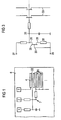
- FIG. 3 A circuit known in the prior art which partially stabilizes the quiescent current is shown in FIG. 3.
- a component in which this circuit arrangement is used is sold under the name CGY-96 by Siemens AG.
- field effect transistor 25, resistor 32 and V neg 29 form a constant current source .
- Drain terminal 26 is connected via a resistor to the positive voltage V con 27.
- This circuit arrangement is connected via connection 31 to the gates of the final stage field effect transistors 33 of the amplifier circuit. All components that form the circuit in FIG. 3 are located on a chip made in MMIC technology.
- the control circuit for controlling the quiescent current is arranged in a separate circuit section at a distance of far more than 500 ⁇ m from the output stage transistors.
- the disadvantage of this arrangement is that the customer must calibrate the amplifier circuit at point 27 (V con ). It is also disadvantageous that the drain current has a non-linear dependence on voltage V con 27.
- the object of the present invention is now to compare one the arrangement described above improved amplifier circuit to provide that is not subsequently calibrated must be and over a significantly expanded temperature range has a quiescent current, which within the predetermined limits.
- the present invention therefore relates to an amplifier circuit comprising at least one output stage transistor 12, a circuit for compensating for quiescent current drifts and if necessary, components for controlling the output stage transistor (s), which is characterized in that the circuit to compensate for quiescent current drifts at least one reference current field effect transistor 23 with a gate electrode 22 having at least one gate electrode 22 in the region of the electrodes of the output stage transistor (s) 5 and the reference current field effect transistor (s) on a common chip area 6,8 with the output stage transistor (s) 12 is located.
- the reference current transistor according to the present invention is designed in such a way that it relates to the outside Quiescent current electrical and physical influences sensitive to the output stage transistors as well as possible.
- the reference current transistor is preferably on the same electrical potential as the output stage transistors.
- the amplifier circuit according to the invention preferably has a quiescent current in the temperature range from -30 ° C to 80 ° C is in a range from 10 to 500 mA.
- the gate electrode 22 is preferably at a distance of less than 100 ⁇ m from the next electrode 5 one Power transistor removed. Is particularly preferred the gate electrode 22 at a distance of less than 50 ⁇ m arranged.
- a transistor is used as the reference current transistor 23, which is preferably of the type of the output stage transistor (s) 12 largely corresponds.
- both are Types of transistors manufactured using GaAs MESFET technology.
- the current of the reference current transistor (s) is preferably to control the input signal of the output stage transistor (s) used.
- the circuit for compensating for quiescent current drifts is in one preferred embodiment not arranged on the chip 6,8, on which the output stage transistors 12 are located.
- the circuit for compensating quiescent current drifts preferably forms with the help of a largely constant Reference voltage 13 and a resistor 14 one the current of the reference current transistors proportional voltage 20. This voltage is then used to regulate the input signal of the output stage transistor / s used.
- This Transistor is particularly preferably a bipolar transistor, in particular a PNP transistor in bipolar technology.
- circuit for compensating quiescent current drifts expediently an additional circuit arrangement 17, 18, which additionally existing temperature drifts Compensation circuit compensated.
- Another object of the present invention is Use of the amplifier circuit according to the invention as a power amplifier in cellular systems, such as cellular phones.
- FIG. 1 shows the high-frequency part of an amplifier circuit according to the invention.
- the output stage transistors are preferably HF-FETs, such as GaAs-MESFETs.
- V neg 1 is connected via a resistor to a capacitor and gate 22 of the reference current transistor.
- Bondpad 2 is connected to gate 22 of the reference current transistor via a further resistor.
- Bondpad 3 is connected to drain finger 4 of the reference current transistor.
- the reference current transistor is connected to the individual amplifier stages as a current mirror.
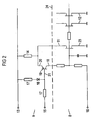
- line 24 defines a spatial and circuit-technical separation of area 8 (chip) from area 9 (external circuit area).
- Node 10 corresponds to connection gate 2 in FIG. 1 and node 11 to drain 3 in FIG. 1.
- a voltage is present at V ref 13, which is preferably stabilized and is, for example, approximately +3 V. The fluctuations are expediently less than + -5%.
- the potential at point V con 15 is in the range from 0 to 2 V.
- At point V neg 16 there is a voltage of approximately -4 V.
- the resistor R ref 14 is connected to the emitter 20 of the transistor 19 and to the reference current transistor 23 (drain). For example, a voltage of +1 V is present at R ref 14.
- the voltage at point 20 is then +2 V, that at base 21 is +1.3 V.
- a PNP double transistor in bipolar technology can be used as a component for control 19.
- temperature compensation of the component for regulation 19 can preferably be carried out.
- V ref 13 is connected to diode 18 via resistor 17.
- diode 18 is connected to base 21 and via a resistor to V con 15.
- the compensation circuit according to the invention makes this possible Regulation of a constant quiescent current over a wide temperature range.
- the current physical conditions in the The area of the output stage transistors are characterized by the extensive spatial and geometric correspondence of the reference current transistor particularly precise with the output stage transistors and modeled without delay.
- the circuit also offers the advantage that the reference current transistor the same electrical potential as the output stage transistors lies.
- the amplifier circuit according to the invention is also advantageous compared to known amplifier circuits, since an optimal thermal coupling of the reference current transistor to the thermally active output stage transistors. in addition comes that this achieves advantages in dynamic operation become.
- Another advantage of the amplifier circuit according to the invention is the reduction in the amount of negative required Auxiliary voltage.
- the amplifier circuit according to the invention offers advantages in particular when on-chip resistors are used which are subject to relatively high tolerances. Corresponding on-chip resistors have practically no influence on the controlled variable in the amplifier circuit according to the invention. In addition, a reduction in the time required for production can be achieved during the production of the amplifier circuit according to the invention, since a selection of the exposure masks required during production can be omitted.
Landscapes
- Engineering & Computer Science (AREA)
- Power Engineering (AREA)
- Amplifiers (AREA)
Description
- Figur 1
- ein Beispiel für eine erfindungsgemäße. Schaltungsanordnung auf einem Chip 6, 8,
- Figur 2
- eine Schaltungsanordnung gemäß der Erfindung mit dem in Fig. 1 gezeigten Schaltungsteil auf dem Chip 6, 8 und einer Kompensationsschaltung 9 und
- Figur 3
- eine Schaltungsanordnung zur Anpassung des Ruhestroms basierend auf einer Konstantstromquelle gemäß dem Stand der Technik.
Weiterhin befinden sich auf dem Chip 6 Bondpads für Vneg 1, Gate 2 und Drain 3. Vneg 1 ist über einen Widerstand mit einem Kondensator und Gate 22 des Referenzstromtransistors verbunden. Bondpad 2 ist mit Gate 22 des Referenzstromtransistors über einen weiteren Widerstand verbunden. Desweiteren besteht über einen Widerstand eine Verbindung zu den Gates der Endstufentransistoren 5. Bondpad 3 ist mit Drain-Finger 4 des Referenzstromtransistors verbunden. An Schaltungspunkt 7 besteht eine Verbindung zu weiteren Gates. Der Referenzstromtransistor ist mit den einzelnen Verstärkerstufen als Stromspiegel beschaltet.
Schaltungspunkt 10 entspricht Anschluß Gate 2 in Figur 1 und Schaltungspunkt 11 Anschluß Drain 3 in Figur 1.
An Vref 13 liegt eine Spannung an, die vorzugsweise stabilisiert ist und beispielsweise bei etwa +3 V liegt. Die Schwankungen betragen zweckmäßigerweise weniger als +-5%. Das Potential an Punkt Vcon 15 liegt im Bereich von 0 bis 2 V. An Punkt Vneg 16 liegt eine Spannung von etwa -4 V an. Der Widerstand Rref 14 ist mit Emitter 20 des Transistors 19 und mit Referenzstromtransistor 23 (Drain) verbunden.
An Rref 14 liegt beispielsweise eine Spannung von +1 V an. Die Spannung an Punkt 20 beträgt dann +2 V, die an Basis 21 +1,3 V.
Zusätzlich kann während der Fertigung der erfindungsgemäßen Verstärkerschaltung eine Reduktion des zur Fertigung erforderlichen Zeitaufwands erreicht werden, da eine Selektion der bei der Fertigung erforderlichen Belichtungsmasken entfallen kann.
Claims (7)
- Verstärkerschaltung umfassend mindestens einen Endstufentransistor (12), eine Schaltung zur Kompensation von Ruhestromdrifts und ggf. Bauelemente zur Ansteueung des/der Endstufentransistor-s/-en,
dadurch gekennzeichnet, daß die Schaltung zur Kompensation von Ruhestromdriftsmindestens einen Referenzstromfeldeffekttransistor (23) mit einer Gateleektrode (22) aufweist, wobei mindestens eine Gateelektrode (22) im Bereich der Elektroden des/der Endstufentransistor-s/-en (5) angeordnet ist und sich der/die Referenzstromfeldeffekttransistor/-en auf einer gemeinsamen Chipfläche (6, 8) mit dem/den Endstufentransistor/-en (12) befindet, wobei sich die Gateelektrode (22) in einem Abstand von weniger als 100 µm von der nächsten Elektrode (5) eines Endstufentransistors befindet; undeine zusätzliche Schaltungsanordnung (17, 18) aufweist, welche zusätzlich vorhandene Temperaturdrifts der Kompensationsschaltung kompensiert. - Verstärkerschaltung nach Anspruch 1,
dadurch gekennzeichnet, daß die Bauart des Referenzstromtransistors (23) der Bauart der Endstufentransistoren (12) weitestgehend entspricht. - Verstärkerschaltung nach Anspruch 1 oder 2,
dadurch gekennzeichnet, daß der Strom des/der Refenzstromtransistor-s-en zur Regelung des Eingangssignals des/der Endstufentransistors/-en benutzt wird. - Verstärkerschaltung nach mindestens einem der Ansprüche 1 bis 3,
dadurch gekennzeichnet, daß die Schaltung zur Kompensation von Ruhestromdrifts bis auf mindestens einen Referenzstromfeldeffekttransistor (23) nicht auf dem Chip (6, 8) angeordnet ist, auf dem sich die Endstufentransistoren (12) befinden. - Verstärkerschaltung nach mindestens einem der Ansprüche 1 bis 4,
dadurch gekennzeichnet, daß die Schaltung zur Kompensation von Ruhestromdrifts unter Zuhilfenahme einer weitgehend konstanten Referenzspannung (13) und eines Widerstandes (14) eine dem Strom des/der Referenzstromtransistor-s-en proportionale Spannung (20) bildet, welche zur Regelung des Eingangssignals des/der Endstufentransistor-s/-en benutzt wird. - Verstärkerschaltung nach mindestens einem der Ansprüche 1 bis 5,
dadurch gekennzeichnet, daß die Schaltung zur Kompensation von Ruhestromdrifts zur Regelung des Eingangssignals des/der Endstufentransistor-s/en mindestens einen Transistor (19) in bipolarer Technologie aufweist. - Verwendung der Verstärkerschaltung nach Anspruch 1 in Mobilfunkanlagen
Applications Claiming Priority (3)
| Application Number | Priority Date | Filing Date | Title |
|---|---|---|---|
| DE19827702A DE19827702C2 (de) | 1998-06-22 | 1998-06-22 | Verstärkerschaltung mit aktiver Arbeitspunkteinstellung |
| DE19827702 | 1998-06-22 | ||
| PCT/DE1999/001679 WO1999067879A1 (de) | 1998-06-22 | 1999-06-08 | Aktive arbeitspunkteeinstellung für leistungsverstärker |
Publications (2)
| Publication Number | Publication Date |
|---|---|
| EP1004165A1 EP1004165A1 (de) | 2000-05-31 |
| EP1004165B1 true EP1004165B1 (de) | 2004-03-03 |
Family
ID=7871613
Family Applications (1)
| Application Number | Title | Priority Date | Filing Date |
|---|---|---|---|
| EP99938146A Expired - Lifetime EP1004165B1 (de) | 1998-06-22 | 1999-06-08 | Aktive arbeitspunkteeinstellung für leistungsverstärker |
Country Status (8)
| Country | Link |
|---|---|
| US (1) | US6255910B1 (de) |
| EP (1) | EP1004165B1 (de) |
| JP (1) | JP2002519882A (de) |
| KR (1) | KR20010023199A (de) |
| CA (1) | CA2302692A1 (de) |
| DE (2) | DE19827702C2 (de) |
| TW (1) | TW449961B (de) |
| WO (1) | WO1999067879A1 (de) |
Families Citing this family (14)
| Publication number | Priority date | Publication date | Assignee | Title |
|---|---|---|---|---|
| DE10002371A1 (de) * | 2000-01-20 | 2001-08-09 | Infineon Technologies Ag | Verstärkerschaltung |
| FR2834088B1 (fr) * | 2001-12-20 | 2004-03-19 | St Microelectronics Sa | Procede et dispositif de polarisation d'un transistor d'un etage amplificateur radiofrequence |
| DE10212165A1 (de) * | 2002-03-19 | 2003-10-09 | Infineon Technologies Ag | Transistoranordnung |
| US20050128003A1 (en) * | 2002-03-19 | 2005-06-16 | Infineon Technologies Ag | Transistor assembly |
| GB2406728B (en) * | 2003-10-01 | 2007-06-13 | Zarlink Semiconductor Ltd | An integrated circuit device |
| GB2408400B (en) * | 2003-11-24 | 2006-05-03 | Zarlink Semiconductor Ltd | A circuit arrangement |
| GB2408401B (en) * | 2003-11-24 | 2006-05-03 | Zarlink Semiconductor Ltd | A network |
| DE102004021155B3 (de) | 2004-04-29 | 2005-12-29 | Infineon Technologies Ag | Wanderwellenverstärker |
| US7671684B2 (en) | 2005-07-05 | 2010-03-02 | Japan Radio Co., Ltd. | FET bias circuit |
| US7768353B2 (en) | 2008-06-13 | 2010-08-03 | Samsung Electro-Mechanics Company, Ltd. | Systems and methods for switching mode power amplifier control |
| US8884700B2 (en) * | 2013-01-17 | 2014-11-11 | Raytheon Company | Integrated circuit chip temperature sensor |
| JP5997633B2 (ja) * | 2013-03-18 | 2016-09-28 | アズビル株式会社 | 電磁流量計 |
| CN106443123A (zh) * | 2016-08-29 | 2017-02-22 | 武汉邮电科学研究院 | 用于移动通信的功率放大器静态工作点测量方法及系统 |
| DE102023207185A1 (de) * | 2023-07-27 | 2025-01-30 | Carl Zeiss Smt Gmbh | Ansteuervorrichtung, optisches system und lithographieanlage |
Family Cites Families (10)
| Publication number | Priority date | Publication date | Assignee | Title |
|---|---|---|---|---|
| DE2705583C2 (de) * | 1977-02-10 | 1982-04-08 | Siemens AG, 1000 Berlin und 8000 München | Transistorschaltung mit einem vor thermischer Zerstörung zu schützenden Transistor |
| US5216383A (en) * | 1991-05-21 | 1993-06-01 | U.S. Philips Corporation | Controllable amplifier circuit |
| DE4128713A1 (de) | 1991-08-29 | 1993-03-04 | Daimler Benz Ag | Verfahren und anordnung zur messung der traegerfrequenzablage in einem mehrkanaluebertragungssystem |
| DE69427378T2 (de) * | 1993-01-08 | 2002-04-25 | Sony Corp., Tokio/Tokyo | Monolithische integrierte Mikrowellenschaltung |
| JPH0742577U (ja) * | 1993-12-28 | 1995-08-04 | ミツミ電機株式会社 | 増幅器 |
| JPH0846446A (ja) * | 1994-07-29 | 1996-02-16 | Oki Electric Ind Co Ltd | ゲートバイアス回路 |
| GB2307155B (en) | 1995-11-02 | 1999-09-15 | British Broadcasting Corp | Synchronisation of OFDM signals |
| JP3657079B2 (ja) * | 1997-03-19 | 2005-06-08 | 富士通株式会社 | エンハンスメント型トランジスタ回路のバイアス回路を有する集積回路装置 |
| US5952886A (en) * | 1998-01-20 | 1999-09-14 | Motorola, Inc. | MMIC power amplifier with diagonal circuitry |
| US6046642A (en) * | 1998-09-08 | 2000-04-04 | Motorola, Inc. | Amplifier with active bias compensation and method for adjusting quiescent current |
-
1998
- 1998-06-22 DE DE19827702A patent/DE19827702C2/de not_active Expired - Fee Related
-
1999
- 1999-06-08 KR KR1020007001827A patent/KR20010023199A/ko not_active Withdrawn
- 1999-06-08 WO PCT/DE1999/001679 patent/WO1999067879A1/de not_active Ceased
- 1999-06-08 CA CA002302692A patent/CA2302692A1/en not_active Abandoned
- 1999-06-08 EP EP99938146A patent/EP1004165B1/de not_active Expired - Lifetime
- 1999-06-08 DE DE59908714T patent/DE59908714D1/de not_active Expired - Fee Related
- 1999-06-08 JP JP2000556444A patent/JP2002519882A/ja active Pending
- 1999-06-16 TW TW088110080A patent/TW449961B/zh active
-
2000
- 2000-02-22 US US09/510,642 patent/US6255910B1/en not_active Expired - Fee Related
Also Published As
| Publication number | Publication date |
|---|---|
| EP1004165A1 (de) | 2000-05-31 |
| CA2302692A1 (en) | 1999-12-22 |
| WO1999067879A1 (de) | 1999-12-29 |
| KR20010023199A (ko) | 2001-03-26 |
| DE59908714D1 (de) | 2004-04-08 |
| DE19827702A1 (de) | 1999-12-30 |
| TW449961B (en) | 2001-08-11 |
| JP2002519882A (ja) | 2002-07-02 |
| DE19827702C2 (de) | 2000-06-08 |
| US6255910B1 (en) | 2001-07-03 |
Similar Documents
| Publication | Publication Date | Title |
|---|---|---|
| EP1004165B1 (de) | Aktive arbeitspunkteeinstellung für leistungsverstärker | |
| DE69427311T2 (de) | Vorspannungsstabilisierungsschaltung | |
| DE69325293T2 (de) | Differenzverstärker mit verbesserter Gleichtaktstabilität | |
| DE3523400C2 (de) | Schaltungsanordnung für eine Ausgangsstufe der Klasse AB mit großer Schwingungsweite | |
| EP0721269B1 (de) | Integrierte CMOS-Schaltung | |
| EP1321843B1 (de) | Stromquellenschaltung | |
| DE60217504T2 (de) | Verstärker mit variabler verstärkung für einen offenen regelkreis unter verwendung einer replikatverstärkerzelle | |
| DE69428884T2 (de) | Überlastschutzschaltkreis für MOS-Leistungstreiber | |
| DE2254618B2 (de) | Integrierte spannungsregelschaltung | |
| DE60224799T2 (de) | Verfahren und vorrichtung zur kalibration einer gm zelle unter verwendung einer gm replikatzelle | |
| DE102009004833A1 (de) | Halbleiterleistungselement mit Vorspannungsschalter | |
| DE69917822T2 (de) | Operationsverstärker | |
| DE3832448A1 (de) | Messverstaerker mit programmierbarer verstaerkung | |
| DE10066032A1 (de) | Schaltungsanordnung zur Steuerung der Verstärkung einer Verstärkerschaltung | |
| DE3856194T2 (de) | Verstärkerschaltung und mit der Verstärkerschaltung versehene Wiedergabeanordnung | |
| EP1264396B1 (de) | Schaltungsanordnung zur arbeitspunkteinstellung eines hochfrequenztransistors und verstärkerschaltung | |
| DE69934828T2 (de) | Gate-vorspannungsvorrichtung | |
| EP0556644B1 (de) | Integrierte Schaltungsanordnung | |
| DE4331499A1 (de) | Schwingkreis | |
| DE3924471A1 (de) | Breitbandverstaerker mit stromspiegelrueckgekoppelter vorspannungsschaltung | |
| DE3017654C2 (de) | ||
| EP0990199B1 (de) | Reglervorrichtung | |
| EP1148634B1 (de) | Verstärkerschaltung | |
| DE69418206T2 (de) | Verfahren zur Spannungsschwelleextraktierung und Schaltung nach dem Verfahren | |
| DE19940382A1 (de) | Stromquelle für niedrige Betriebsspannungen mit hohem Ausgangswiderstand |
Legal Events
| Date | Code | Title | Description |
|---|---|---|---|
| PUAI | Public reference made under article 153(3) epc to a published international application that has entered the european phase |
Free format text: ORIGINAL CODE: 0009012 |
|
| 17P | Request for examination filed |
Effective date: 20000218 |
|
| AK | Designated contracting states |
Kind code of ref document: A1 Designated state(s): CH DE FI FR GB IT LI NL SE |
|
| 17Q | First examination report despatched |
Effective date: 20020321 |
|
| GRAP | Despatch of communication of intention to grant a patent |
Free format text: ORIGINAL CODE: EPIDOSNIGR1 |
|
| GRAS | Grant fee paid |
Free format text: ORIGINAL CODE: EPIDOSNIGR3 |
|
| GRAA | (expected) grant |
Free format text: ORIGINAL CODE: 0009210 |
|
| AK | Designated contracting states |
Kind code of ref document: B1 Designated state(s): CH DE FI FR GB IT LI NL SE |
|
| PG25 | Lapsed in a contracting state [announced via postgrant information from national office to epo] |
Ref country code: NL Free format text: LAPSE BECAUSE OF FAILURE TO SUBMIT A TRANSLATION OF THE DESCRIPTION OR TO PAY THE FEE WITHIN THE PRESCRIBED TIME-LIMIT Effective date: 20040303 Ref country code: IT Free format text: LAPSE BECAUSE OF FAILURE TO SUBMIT A TRANSLATION OF THE DESCRIPTION OR TO PAY THE FEE WITHIN THE PRE;WARNING: LAPSES OF ITALIAN PATENTS WITH EFFECTIVE DATE BEFORE 2007 MAY HAVE OCCURRED AT ANY TIME BEFORE 2007. THE CORRECT EFFECTIVE DATE MAY BE DIFFERENT FROM THE ONE RECORDED.SCRIBED TIME-LIMIT Effective date: 20040303 Ref country code: FI Free format text: LAPSE BECAUSE OF FAILURE TO SUBMIT A TRANSLATION OF THE DESCRIPTION OR TO PAY THE FEE WITHIN THE PRESCRIBED TIME-LIMIT Effective date: 20040303 |
|
| REG | Reference to a national code |
Ref country code: GB Ref legal event code: FG4D Free format text: NOT ENGLISH |
|
| REG | Reference to a national code |
Ref country code: CH Ref legal event code: EP |
|
| REF | Corresponds to: |
Ref document number: 59908714 Country of ref document: DE Date of ref document: 20040408 Kind code of ref document: P |
|
| GBT | Gb: translation of ep patent filed (gb section 77(6)(a)/1977) |
Effective date: 20040414 |
|
| PG25 | Lapsed in a contracting state [announced via postgrant information from national office to epo] |
Ref country code: SE Free format text: LAPSE BECAUSE OF FAILURE TO SUBMIT A TRANSLATION OF THE DESCRIPTION OR TO PAY THE FEE WITHIN THE PRESCRIBED TIME-LIMIT Effective date: 20040603 |
|
| PG25 | Lapsed in a contracting state [announced via postgrant information from national office to epo] |
Ref country code: GB Free format text: LAPSE BECAUSE OF NON-PAYMENT OF DUE FEES Effective date: 20040608 |
|
| PG25 | Lapsed in a contracting state [announced via postgrant information from national office to epo] |
Ref country code: LI Free format text: LAPSE BECAUSE OF NON-PAYMENT OF DUE FEES Effective date: 20040630 Ref country code: CH Free format text: LAPSE BECAUSE OF NON-PAYMENT OF DUE FEES Effective date: 20040630 |
|
| NLV1 | Nl: lapsed or annulled due to failure to fulfill the requirements of art. 29p and 29m of the patents act | ||
| ET | Fr: translation filed | ||
| PLBE | No opposition filed within time limit |
Free format text: ORIGINAL CODE: 0009261 |
|
| STAA | Information on the status of an ep patent application or granted ep patent |
Free format text: STATUS: NO OPPOSITION FILED WITHIN TIME LIMIT |
|
| GBPC | Gb: european patent ceased through non-payment of renewal fee |
Effective date: 20040608 |
|
| REG | Reference to a national code |
Ref country code: CH Ref legal event code: PL |
|
| 26N | No opposition filed |
Effective date: 20041206 |
|
| PGFP | Annual fee paid to national office [announced via postgrant information from national office to epo] |
Ref country code: DE Payment date: 20060808 Year of fee payment: 8 |
|
| PG25 | Lapsed in a contracting state [announced via postgrant information from national office to epo] |
Ref country code: DE Free format text: LAPSE BECAUSE OF NON-PAYMENT OF DUE FEES Effective date: 20080101 |
|
| PG25 | Lapsed in a contracting state [announced via postgrant information from national office to epo] |
Ref country code: FR Free format text: LAPSE BECAUSE OF NON-PAYMENT OF DUE FEES Effective date: 20040630 |
|
| REG | Reference to a national code |
Ref country code: FR Ref legal event code: ST Effective date: 20110923 |