EP1005012A1 - Digitale Addressierung einer flache Anzeigetafel - Google Patents
Digitale Addressierung einer flache Anzeigetafel Download PDFInfo
- Publication number
- EP1005012A1 EP1005012A1 EP99410169A EP99410169A EP1005012A1 EP 1005012 A1 EP1005012 A1 EP 1005012A1 EP 99410169 A EP99410169 A EP 99410169A EP 99410169 A EP99410169 A EP 99410169A EP 1005012 A1 EP1005012 A1 EP 1005012A1
- Authority
- EP
- European Patent Office
- Prior art keywords
- addressing
- electrode
- time
- during
- potential
- Prior art date
- Legal status (The legal status is an assumption and is not a legal conclusion. Google has not performed a legal analysis and makes no representation as to the accuracy of the status listed.)
- Granted
Links
- 230000035945 sensitivity Effects 0.000 claims abstract description 11
- 239000011159 matrix material Substances 0.000 claims abstract description 5
- 238000000034 method Methods 0.000 claims description 22
- 238000005286 illumination Methods 0.000 claims description 10
- 238000012800 visualization Methods 0.000 claims description 2
- 230000001105 regulatory effect Effects 0.000 abstract 1
- 230000006870 function Effects 0.000 description 7
- 238000010586 diagram Methods 0.000 description 5
- 230000004044 response Effects 0.000 description 4
- 230000008901 benefit Effects 0.000 description 3
- 230000008569 process Effects 0.000 description 3
- 230000001143 conditioned effect Effects 0.000 description 2
- 230000005669 field effect Effects 0.000 description 2
- 238000012986 modification Methods 0.000 description 2
- 230000004048 modification Effects 0.000 description 2
- 230000008447 perception Effects 0.000 description 2
- 239000003086 colorant Substances 0.000 description 1
- 230000000694 effects Effects 0.000 description 1
- 230000006872 improvement Effects 0.000 description 1
- 239000004973 liquid crystal related substance Substances 0.000 description 1
- 238000009877 rendering Methods 0.000 description 1
- 238000005070 sampling Methods 0.000 description 1
- 230000017105 transposition Effects 0.000 description 1
Images
Classifications
-
- G—PHYSICS
- G09—EDUCATION; CRYPTOGRAPHY; DISPLAY; ADVERTISING; SEALS
- G09G—ARRANGEMENTS OR CIRCUITS FOR CONTROL OF INDICATING DEVICES USING STATIC MEANS TO PRESENT VARIABLE INFORMATION
- G09G3/00—Control arrangements or circuits, of interest only in connection with visual indicators other than cathode-ray tubes
- G09G3/20—Control arrangements or circuits, of interest only in connection with visual indicators other than cathode-ray tubes for presentation of an assembly of a number of characters, e.g. a page, by composing the assembly by combination of individual elements arranged in a matrix no fixed position being assigned to or needed to be assigned to the individual characters or partial characters
- G09G3/22—Control arrangements or circuits, of interest only in connection with visual indicators other than cathode-ray tubes for presentation of an assembly of a number of characters, e.g. a page, by composing the assembly by combination of individual elements arranged in a matrix no fixed position being assigned to or needed to be assigned to the individual characters or partial characters using controlled light sources
-
- G—PHYSICS
- G09—EDUCATION; CRYPTOGRAPHY; DISPLAY; ADVERTISING; SEALS
- G09G—ARRANGEMENTS OR CIRCUITS FOR CONTROL OF INDICATING DEVICES USING STATIC MEANS TO PRESENT VARIABLE INFORMATION
- G09G2310/00—Command of the display device
- G09G2310/06—Details of flat display driving waveforms
- G09G2310/066—Waveforms comprising a gently increasing or decreasing portion, e.g. ramp
-
- G—PHYSICS
- G09—EDUCATION; CRYPTOGRAPHY; DISPLAY; ADVERTISING; SEALS
- G09G—ARRANGEMENTS OR CIRCUITS FOR CONTROL OF INDICATING DEVICES USING STATIC MEANS TO PRESENT VARIABLE INFORMATION
- G09G2320/00—Control of display operating conditions
- G09G2320/02—Improving the quality of display appearance
- G09G2320/0271—Adjustment of the gradation levels within the range of the gradation scale, e.g. by redistribution or clipping
- G09G2320/0276—Adjustment of the gradation levels within the range of the gradation scale, e.g. by redistribution or clipping for the purpose of adaptation to the characteristics of a display device, i.e. gamma correction
-
- G—PHYSICS
- G09—EDUCATION; CRYPTOGRAPHY; DISPLAY; ADVERTISING; SEALS
- G09G—ARRANGEMENTS OR CIRCUITS FOR CONTROL OF INDICATING DEVICES USING STATIC MEANS TO PRESENT VARIABLE INFORMATION
- G09G3/00—Control arrangements or circuits, of interest only in connection with visual indicators other than cathode-ray tubes
- G09G3/20—Control arrangements or circuits, of interest only in connection with visual indicators other than cathode-ray tubes for presentation of an assembly of a number of characters, e.g. a page, by composing the assembly by combination of individual elements arranged in a matrix no fixed position being assigned to or needed to be assigned to the individual characters or partial characters
- G09G3/2007—Display of intermediate tones
- G09G3/2011—Display of intermediate tones by amplitude modulation
-
- G—PHYSICS
- G09—EDUCATION; CRYPTOGRAPHY; DISPLAY; ADVERTISING; SEALS
- G09G—ARRANGEMENTS OR CIRCUITS FOR CONTROL OF INDICATING DEVICES USING STATIC MEANS TO PRESENT VARIABLE INFORMATION
- G09G3/00—Control arrangements or circuits, of interest only in connection with visual indicators other than cathode-ray tubes
- G09G3/20—Control arrangements or circuits, of interest only in connection with visual indicators other than cathode-ray tubes for presentation of an assembly of a number of characters, e.g. a page, by composing the assembly by combination of individual elements arranged in a matrix no fixed position being assigned to or needed to be assigned to the individual characters or partial characters
- G09G3/2007—Display of intermediate tones
- G09G3/2014—Display of intermediate tones by modulation of the duration of a single pulse during which the logic level remains constant
Definitions
- the present invention relates to flat screens of visualization. It relates more particularly to screens dishes in which the respective lighting instructions for different pixels are applied digitally to an electrode of the screen.
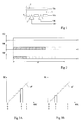
- FIG. 1 very schematically and partially represents the structure of a flat screen with microtips.
- This screen includes electrodes cathode, here microtips 1, intended to emit electrons to anode 2 electrodes separated from the cathodes by a space vacuum 3.
- Grid electrodes 4 are associated with the electrodes of cathode 1, generally in a perpendicular direction, so to form an electron-emitting matrix network.
- microtip screen of the type to which it applies the present invention and its operating principle are described in American patent n ° 4940916 of the Commissariat à Atomic Energy.
- Figure 1 is very schematic. In particular, this representation aims to distinguish the different addressing potentials of the electrodes and not to explain in detail the structure of the microtip screen. Thus, in Figure 1, only one microtip per pixel has been represented while the microtips are, in practice, among the number several thousand per pixel of screen.
- the anode 2 is brought to a potential V A (for example, several hundred volts) substantially higher than the potential of the cathode to attract the electrons emitted by the microtips.
- V A for example, several hundred volts
- the anode is, in general, permanently brought to its addressing potential.
- three anodes of different colors blue, green, red are generally used which are then addressed sequentially by frame of each color.
- the grid electrodes 4 are organized in rows in a first direction and are sequentially polarized, in a line scan, at an addressing potential, generally at a potential V G , positive with respect to the cathode electrodes 1.
- the cathode electrodes 1 are organized in columns in a second direction perpendicular to the first and are simultaneously addressed by respective signals V K , V K , during the addressing of a grid line, the electron emission current representing, for each grid row, the brightness of the pixel defined by the intersection of the cathode column and the grid row.
- the addressing potential cathode electrodes represents the brightness of the pixel defined by the intersection of the cathode column and the row of the grid.
- the columns are therefore brought to potentials between a maximum emission potential and a no emission potential (for example 0 and 30 respectively volts for a grid whose addressing potential is around 80 volts).
- the gloss is defined by addressing time (addressing pulse width) of the column considered during the addressing time (line time) of the grid.
- FIG. 2 illustrates, very schematically and in the form of timing diagrams, an example of cathode addressing by pulse width modulation.
- all the cathode columns are, during the addressing time tl of each grid line 4, addressed by respective signals V K , V K ' , each corresponding to a pulse whose width is function of the desired illumination for the pixel defined by the intersection of the row and the column considered.
- the column addressed by the signal V K has a greater lighting setpoint than that addressed by the signal V K insofar as the periods during which the potential difference between the gate electrode and the cathode electrode is high (for example, above the threshold of 50 volts of electron emission) are more important.
- maximum illumination generally corresponds to a minimum pulse width. Note however that it is enough to reverse the pulse to obtain a different illumination rule as a function of the pulse widths, and that the principle of pulse width modulation for fixing the quantity of electrons emitted remains the even.
- the modulation of the width of the addressing pulses of the cathode electrodes is most often carried out digitally.
- the respective light intensities I K , and I K of the pixels considered above are fixed by binary words, respectively W K , and W K.
- the higher the desired light intensity the higher the binary word represents a number (for example 1.0.1 for column K 'and 0.1.1. For column K).
- Digital addressing is particularly suitable for matrix screens in which one of the electrodes is addressed by impulse signals whose pulse width fixes the gloss setpoint. Indeed, this pulse width modulation is generally done from a clock (dotted, Figure 2) higher frequency than that of pulse trains generally corresponding to the line scan frequency, so the more often by cutting into whole numbers of clock cycles.
- An object of the present invention is to improve perception user lighting levels in the levels dark.
- the present invention also aims to propose a new digital addressing process for a display screen which implements such an improvement.
- the present invention also aims to propose a method whose implementation is particularly simple and which minimizes changes to traditional digital addressing of such a screen.
- the present invention provides a method of digital addressing of a flat display screen organized in a matrix network and including at least a first electrode receives a digital lighting command setting the width of pulses to be applied during an addressing time of a second perpendicular electrode, this process consisting in rendering non-constant the amplitude of light emission during the address time of the second electrode.
- said non-constant variation follows a law established from of the relationship between the sensitivity of the eye to light.
- the process is applied to a flat display screen in which the first electrode is constituted by a cathode with field emission, the second electrode consisting of a grid associated with the cathode.
- the method consists in varying the addressing potential of the second electrode during said addressing time.
- the method consists in increasing non-linearly the addressing potential of the grid lines during each time line.
- the method consists in varying the frequency of a clock modulation pulse width addressing the first electrode.
- the clock frequency variation is carried out modulo the addressing time of the second electrode.
- the method consists in varying the addressing potential of a third electrode during the addressing time of the second electrode.
- the third electrode is constituted by a cathodoluminescent anode.
- the method consists in varying the addressing voltage of the first electrode during the addressing time of the second electrode.
- the present invention originates from an observation the sensitivity of the eye as a function of the illumination.
- This sensitivity is not linear but is approximately logarithmic, that is to say that two neighboring gray levels are distinguished better if they are dark than if they are light.
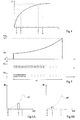
- Figure 4 illustrates the influence of this sensitivity logarithmic of the eye on the addressing of a screen digitally. This figure represents the response of eye E as a function of light intensity L.
- the intensity axis light I is cut (sampled) to code this intensity in binary form, for example on 3 bits (8 states) in the example represented.
- the non-linearity of the eye's sensitivity to this light intensity leads to two adjacent setpoints (0.0.0, 0.0.1) poor lighting results in responses strongly different from the eye, while two adjacent instructions (1.0.1, 1.1.0) of high light intensity result in eye responses very close to each other.
- the sampling of the luminance setpoints leads to this that two neighboring levels are strongly different from each other in terms of luminance levels (for example, gray levels). he it follows that the differences in levels perceived by the eye are, in the range of lower, lower light intensity levels than the differences in levels recorded.
- a feature of the present invention is to make vary the amplitude of light emission during the addressing time of a scan line.
- FIG. 5 illustrates, in the form of timing diagrams, a first embodiment of the present invention.
- the timing diagrams of FIG. 5 represent the signal V G for addressing a grid line during a line time tl and an example of addressing signals V K and V K ' of cathode columns during this line time.
- the representation of FIG. 5 is to be compared to that of FIG. 2.
- the potential V G for addressing the grid lines is modulated, preferably analogically, during the time tl of selection of each line of the grid.
- the potential of the addressed line is brought to a first value V0 (for example, of the order of 75 volts) and this value increases until reaching a potential V1 (for example, of about 80 volts) at the end of the line time.
- the signals V K and V K ′ for addressing the columns of the cathode are not modified compared to the conventional case (FIG. 2).
- the period during which a cathode emits is the one during which it is brought to a potential low while the grid is brought to a high potential addressing.
- FIGS. 6A and 6B illustrate the effect of the present invention on the respective light intensities I K ' and I K for two binary words, respectively W K' and W K , taken as an example.
- Figures 6A and 6B are to be compared to Figures 3A and 3B set out above.
- the analog modulation of the gate voltage V G results in making the relationship between the light intensity and the binary setpoint non-linear.
- the dotted line pnl shows the interpolation (of increasing slope) of the respective average values of the light intensities as a function of the setpoints.
- the non-linear appearance of this pnl interpolation is to be compared to the dotted line pl of FIGS. 3A and 3B which also represents the interpolation of the mean values of the light intensities but which is linear.
- the non-linearity brought according to the invention to the relation between light intensity and binary setpoint (dotted line pnl), depends on the correction that one wishes to make in depending on the sensitivity of the eye.
- This correction conditioned here by the shape given to the analog modulation of the grid lines potential at each line time tl, will be adapted according to the applications.
- the definition of such pace is within the reach of the skilled person from the indications functional data given above.
- the duration a line time is around 20 to 40 ⁇ s for a screen with classic microtips. This duration is perfectly compatible with the modulation operated according to the present invention.
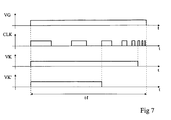
- FIG. 7 illustrates a second embodiment of the present invention. This figure illustrates, in the form of chronograms, the respective patterns of two cathode signals V K and V K ' during a line time tl in which a grid line is addressed by a signal V G.
- a feature of this second mode of implementation is to vary the frequency of the modulation clock CLK the width of each cathode control pulse during the line time. So, as shown in Figure 7, CLK clock signal does not have the same frequency at during a line time. In the embodiment shown, this frequency increases with the passage of time from line.
- the modulation of the width of the pulses of the signals V K and V K ' operated from the clock signal CLK, leads to a non-linearity of the width of these pulses for a difference of the same value of the number of bits of lighting setpoints.
- An advantage of the present invention is that it improves the quality of the images viewed by improving the perception of differences in light levels in the dark regions of a image by reducing the gaps between two consecutive levels.
- Another advantage of the present invention is that it can be implemented in a particularly simple way and with minor modifications to the conventional addressing circuits of viewing screens.
- the present invention is capable of various variants and modifications which will appear to the man of art.
- other means than those described above to vary the light intensity during a line time can be used as long as they respect the functionality described above.
- a such variation which results in a variation of the voltage anode-cathode causes a variation in the emission current, therefore the light intensity during the line time.
- the invention has been described in relation with a screen in which the luminance setpoints are conditioned by the cathode, the transposition of the invention to a screen in which line scanning is carried out on the cathode side is within range of the skilled person.
- the addressing pulses whose one modulates the width could be made up, each, of a train of pulses which, for the second mode of implementation, will have a frequency at least equal to the lowest frequency of the signal CLK of variable frequency.
Landscapes
- Engineering & Computer Science (AREA)
- Physics & Mathematics (AREA)
- Computer Hardware Design (AREA)
- General Physics & Mathematics (AREA)
- Theoretical Computer Science (AREA)
- Control Of Indicators Other Than Cathode Ray Tubes (AREA)
- Devices For Indicating Variable Information By Combining Individual Elements (AREA)
Applications Claiming Priority (2)
| Application Number | Priority Date | Filing Date | Title |
|---|---|---|---|
| FR9815148A FR2786597B1 (fr) | 1998-11-27 | 1998-11-27 | Adressage numerique d'un ecran plat de visualisation |
| FR9815148 | 1998-11-27 |
Publications (2)
| Publication Number | Publication Date |
|---|---|
| EP1005012A1 true EP1005012A1 (de) | 2000-05-31 |
| EP1005012B1 EP1005012B1 (de) | 2006-01-25 |
Family
ID=9533433
Family Applications (1)
| Application Number | Title | Priority Date | Filing Date |
|---|---|---|---|
| EP19990410169 Expired - Lifetime EP1005012B1 (de) | 1998-11-27 | 1999-11-25 | Digitale Addressierung einer flachen Anzeigetafel |
Country Status (4)
| Country | Link |
|---|---|
| EP (1) | EP1005012B1 (de) |
| JP (1) | JP2000163006A (de) |
| DE (1) | DE69929583T2 (de) |
| FR (1) | FR2786597B1 (de) |
Cited By (4)
| Publication number | Priority date | Publication date | Assignee | Title |
|---|---|---|---|---|
| FR2821694A1 (fr) * | 2001-03-01 | 2002-09-06 | Boris Givone | Procede et dispositif permettant d'obtenir une courbe d'energie lumineuse parabolique pour les sources de lumiere electroluminescentes affichant des images sur ecrans geants |
| WO2004059606A3 (en) * | 2002-12-30 | 2004-09-10 | Koninkl Philips Electronics Nv | Line-at-a-time addressed display and drive method |
| EP1480191A2 (de) | 2003-05-19 | 2004-11-24 | Canon Kabushiki Kaisha | Bildanzeigegerät |
| US7710363B2 (en) | 2004-12-28 | 2010-05-04 | Commissariat A L'energie Atomique | Control method for a matrix display screen |
Citations (4)
| Publication number | Priority date | Publication date | Assignee | Title |
|---|---|---|---|---|
| FR2633764A1 (fr) * | 1988-06-29 | 1990-01-05 | Commissariat Energie Atomique | Procede et dispositif de commande d'un ecran matriciel affichant des niveaux de gris |
| FR2708129A1 (fr) * | 1993-07-22 | 1995-01-27 | Commissariat Energie Atomique | Procédé et dispositif de commande d'un écran fluorescent à micropointes. |
| WO1997022132A1 (en) * | 1995-11-30 | 1997-06-19 | Orion Electric Co. Ltd. | Cell driving circuit for use in field emission display |
| FR2749431A1 (fr) * | 1996-05-31 | 1997-12-05 | Pixtech Sa | Reglage de la luminosite d'ensemble d'un ecran matriciel a emission de champ |
Family Cites Families (9)
| Publication number | Priority date | Publication date | Assignee | Title |
|---|---|---|---|---|
| JPS53148918A (en) * | 1977-06-01 | 1978-12-26 | Hitachi Ltd | Matrix display unit |
| JPS57204591A (en) * | 1981-06-12 | 1982-12-15 | Hitachi Ltd | Pulse train generation circuit and pulse width varying signal generation circuit and matrix display unit using them |
| FR2633763B1 (fr) * | 1988-06-29 | 1991-02-15 | Commissariat Energie Atomique | Ecran fluorescent trichrome a micropointes |
| JPH05249920A (ja) * | 1992-02-04 | 1993-09-28 | Nec Corp | 液晶表示装置の駆動回路 |
| FR2698201B1 (fr) * | 1992-11-13 | 1994-12-16 | Commissariat Energie Atomique | Ecran d'affichage matriciel du type multiplexe et son procédé de commande. |
| JPH07181916A (ja) * | 1993-12-22 | 1995-07-21 | Futaba Corp | 表示装置の駆動回路 |
| JP3643659B2 (ja) * | 1996-11-14 | 2005-04-27 | 三洋電機株式会社 | 平面表示装置の駆動方法 |
| US5945968A (en) * | 1997-01-07 | 1999-08-31 | Micron Technology, Inc. | Matrix addressable display having pulsed current control |
| JPH11329721A (ja) * | 1998-05-12 | 1999-11-30 | Tdk Corp | 発光素子の多階調駆動装置および駆動方法 |
-
1998
- 1998-11-27 FR FR9815148A patent/FR2786597B1/fr not_active Expired - Fee Related
-
1999
- 1999-11-18 JP JP11328027A patent/JP2000163006A/ja active Pending
- 1999-11-25 DE DE1999629583 patent/DE69929583T2/de not_active Expired - Lifetime
- 1999-11-25 EP EP19990410169 patent/EP1005012B1/de not_active Expired - Lifetime
Patent Citations (4)
| Publication number | Priority date | Publication date | Assignee | Title |
|---|---|---|---|---|
| FR2633764A1 (fr) * | 1988-06-29 | 1990-01-05 | Commissariat Energie Atomique | Procede et dispositif de commande d'un ecran matriciel affichant des niveaux de gris |
| FR2708129A1 (fr) * | 1993-07-22 | 1995-01-27 | Commissariat Energie Atomique | Procédé et dispositif de commande d'un écran fluorescent à micropointes. |
| WO1997022132A1 (en) * | 1995-11-30 | 1997-06-19 | Orion Electric Co. Ltd. | Cell driving circuit for use in field emission display |
| FR2749431A1 (fr) * | 1996-05-31 | 1997-12-05 | Pixtech Sa | Reglage de la luminosite d'ensemble d'un ecran matriciel a emission de champ |
Cited By (7)
| Publication number | Priority date | Publication date | Assignee | Title |
|---|---|---|---|---|
| FR2821694A1 (fr) * | 2001-03-01 | 2002-09-06 | Boris Givone | Procede et dispositif permettant d'obtenir une courbe d'energie lumineuse parabolique pour les sources de lumiere electroluminescentes affichant des images sur ecrans geants |
| WO2002071381A1 (fr) * | 2001-03-01 | 2002-09-12 | Boris Givone | Procede et dispositif permettant d'obtenir une courbe d'energie lumineuse parabolique pour les sources de lumiere electroluminescentes affichant des images sur ecrans geants |
| WO2004059606A3 (en) * | 2002-12-30 | 2004-09-10 | Koninkl Philips Electronics Nv | Line-at-a-time addressed display and drive method |
| EP1480191A2 (de) | 2003-05-19 | 2004-11-24 | Canon Kabushiki Kaisha | Bildanzeigegerät |
| EP1480191A3 (de) * | 2003-05-19 | 2007-11-28 | Canon Kabushiki Kaisha | Bildanzeigegerät |
| US7423661B2 (en) | 2003-05-19 | 2008-09-09 | Canon Kabushiki Kaisha | Image display apparatus |
| US7710363B2 (en) | 2004-12-28 | 2010-05-04 | Commissariat A L'energie Atomique | Control method for a matrix display screen |
Also Published As
| Publication number | Publication date |
|---|---|
| DE69929583D1 (de) | 2006-04-13 |
| FR2786597B1 (fr) | 2001-02-09 |
| FR2786597A1 (fr) | 2000-06-02 |
| JP2000163006A (ja) | 2000-06-16 |
| DE69929583T2 (de) | 2006-09-28 |
| EP1005012B1 (de) | 2006-01-25 |
Similar Documents
| Publication | Publication Date | Title |
|---|---|---|
| EP0349415B1 (de) | Verfahren und Einrichtung zur Steuerung eines Matrixbildschirmes, der Grauwerte anzeigt | |
| EP0311500B1 (de) | Halbton-Anzeigeverfahren für einen Matrix-Bildschirm | |
| FR2683365A1 (fr) | Dispositif d'affichage a panneau plat a emission de champ et circuit de compensation d'irregulatites utilisable dans un tel dispositif d'affichage. | |
| EP0155895A1 (de) | Verfahren zur Herstellung flacher Bildwiedergabeschirme und nach diesem Verfahren hergestellte Schirme | |
| KR20020085791A (ko) | 비디오 화상 처리를 위한 방법 및 장치 | |
| EP0597772B1 (de) | Multiplexbetriebener Matrixbildschirm und Steuerverfahren dafür | |
| US7940236B2 (en) | Passive matrix electro-luminescent display system | |
| FR2789793A1 (fr) | Affichage d'image a emission de champ | |
| EP0349426B1 (de) | Mikrospitzen-Fluoreszenzbildschirm mit einer geringen Anzahl von Adressierungsschaltkreisen und Adressierungsverfahren von diesem Bildschirm | |
| JP2000221945A (ja) | マトリクス型表示装置 | |
| FR2772502A1 (fr) | Procede de compensation des differences de remanence des luminophores dans un ecran de visualisation d'images | |
| CN100363963C (zh) | 显示图像的方法、显示图像的元件和图像显示设备 | |
| FR2780539A1 (fr) | Dispositif d'affichage d'images | |
| FR2499801A1 (fr) | Dispositif d'affichage d'image de type plat | |
| JP2004309750A (ja) | 表示画面の焼付防止装置及び焼付防止方法 | |
| EP1005012B1 (de) | Digitale Addressierung einer flachen Anzeigetafel | |
| FR2769743A1 (fr) | Procede et dispositif de balayage d'un panneau a plasma | |
| JP2004133400A (ja) | 要求されるよりも少ない映像レベルを表示してディザリングノイズを改善させるプラズマディスプレイパネル(pdp) | |
| EP0292376B1 (de) | Elektrolumineszenzanzeigeeinrichtung mit Speichereffekt und mit Halbton | |
| EP0817232B1 (de) | Verfahren zur Regenerierung von Mikrospitzen einer flachen Anzeigetafel | |
| FR2714209A1 (fr) | Dispositif d'affichage. | |
| EP1677277B1 (de) | Verfahren zur Steuerung einer Matrix-Anzeige | |
| FR2749431A1 (fr) | Reglage de la luminosite d'ensemble d'un ecran matriciel a emission de champ | |
| FR2640407A1 (fr) | Dispositif d'affichage visuel a tube a rayons cathodiques | |
| FR2790861A1 (fr) | Dispositif d'attaque pour dispositif luminescent a emission par effet de champ |
Legal Events
| Date | Code | Title | Description |
|---|---|---|---|
| PUAI | Public reference made under article 153(3) epc to a published international application that has entered the european phase |
Free format text: ORIGINAL CODE: 0009012 |
|
| AK | Designated contracting states |
Kind code of ref document: A1 Designated state(s): DE FR GB IT |
|
| AX | Request for extension of the european patent |
Free format text: AL;LT;LV;MK;RO;SI |
|
| 17P | Request for examination filed |
Effective date: 20001122 |
|
| AKX | Designation fees paid |
Free format text: DE FR GB IT |
|
| 19U | Interruption of proceedings before grant |
Effective date: 20020621 |
|
| 19W | Proceedings resumed before grant after interruption of proceedings |
Effective date: 20050502 |
|
| RAP1 | Party data changed (applicant data changed or rights of an application transferred) |
Owner name: LE COMMISSARIAT AE L'ENERGIE ATOMIQUE |
|
| GRAP | Despatch of communication of intention to grant a patent |
Free format text: ORIGINAL CODE: EPIDOSNIGR1 |
|
| GRAS | Grant fee paid |
Free format text: ORIGINAL CODE: EPIDOSNIGR3 |
|
| GRAA | (expected) grant |
Free format text: ORIGINAL CODE: 0009210 |
|
| RAP1 | Party data changed (applicant data changed or rights of an application transferred) |
Owner name: COMMISSARIAT A L'ENERGIE ATOMIQUE |
|
| AK | Designated contracting states |
Kind code of ref document: B1 Designated state(s): DE FR GB IT |
|
| PG25 | Lapsed in a contracting state [announced via postgrant information from national office to epo] |
Ref country code: IT Free format text: LAPSE BECAUSE OF FAILURE TO SUBMIT A TRANSLATION OF THE DESCRIPTION OR TO PAY THE FEE WITHIN THE PRESCRIBED TIME-LIMIT;WARNING: LAPSES OF ITALIAN PATENTS WITH EFFECTIVE DATE BEFORE 2007 MAY HAVE OCCURRED AT ANY TIME BEFORE 2007. THE CORRECT EFFECTIVE DATE MAY BE DIFFERENT FROM THE ONE RECORDED. Effective date: 20060125 |
|
| REG | Reference to a national code |
Ref country code: GB Ref legal event code: FG4D Free format text: NOT ENGLISH |
|
| REF | Corresponds to: |
Ref document number: 69929583 Country of ref document: DE Date of ref document: 20060413 Kind code of ref document: P |
|
| GBT | Gb: translation of ep patent filed (gb section 77(6)(a)/1977) |
Effective date: 20060524 |
|
| PLBE | No opposition filed within time limit |
Free format text: ORIGINAL CODE: 0009261 |
|
| STAA | Information on the status of an ep patent application or granted ep patent |
Free format text: STATUS: NO OPPOSITION FILED WITHIN TIME LIMIT |
|
| 26N | No opposition filed |
Effective date: 20061026 |
|
| PGFP | Annual fee paid to national office [announced via postgrant information from national office to epo] |
Ref country code: DE Payment date: 20101112 Year of fee payment: 12 |
|
| PGFP | Annual fee paid to national office [announced via postgrant information from national office to epo] |
Ref country code: IT Payment date: 20101125 Year of fee payment: 12 Ref country code: GB Payment date: 20101020 Year of fee payment: 12 |
|
| PGFP | Annual fee paid to national office [announced via postgrant information from national office to epo] |
Ref country code: FR Payment date: 20111215 Year of fee payment: 13 |
|
| GBPC | Gb: european patent ceased through non-payment of renewal fee |
Effective date: 20121125 |
|
| REG | Reference to a national code |
Ref country code: FR Ref legal event code: ST Effective date: 20130731 |
|
| PG25 | Lapsed in a contracting state [announced via postgrant information from national office to epo] |
Ref country code: IT Free format text: LAPSE BECAUSE OF NON-PAYMENT OF DUE FEES Effective date: 20121125 |
|
| REG | Reference to a national code |
Ref country code: DE Ref legal event code: R119 Ref document number: 69929583 Country of ref document: DE Effective date: 20130601 |
|
| PG25 | Lapsed in a contracting state [announced via postgrant information from national office to epo] |
Ref country code: DE Free format text: LAPSE BECAUSE OF NON-PAYMENT OF DUE FEES Effective date: 20130601 |
|
| PG25 | Lapsed in a contracting state [announced via postgrant information from national office to epo] |
Ref country code: GB Free format text: LAPSE BECAUSE OF NON-PAYMENT OF DUE FEES Effective date: 20121125 Ref country code: FR Free format text: LAPSE BECAUSE OF NON-PAYMENT OF DUE FEES Effective date: 20121130 |