EP1480191A2 - Bildanzeigegerät - Google Patents
Bildanzeigegerät Download PDFInfo
- Publication number
- EP1480191A2 EP1480191A2 EP04011829A EP04011829A EP1480191A2 EP 1480191 A2 EP1480191 A2 EP 1480191A2 EP 04011829 A EP04011829 A EP 04011829A EP 04011829 A EP04011829 A EP 04011829A EP 1480191 A2 EP1480191 A2 EP 1480191A2
- Authority
- EP
- European Patent Office
- Prior art keywords
- drive data
- brightness
- data
- modulation
- gradations
- Prior art date
- Legal status (The legal status is an assumption and is not a legal conclusion. Google has not performed a legal analysis and makes no representation as to the accuracy of the status listed.)
- Withdrawn
Links
- 238000012545 processing Methods 0.000 claims description 81
- 238000000034 method Methods 0.000 claims description 60
- 239000011159 matrix material Substances 0.000 claims description 49
- 238000006243 chemical reaction Methods 0.000 claims description 47
- 230000000630 rising effect Effects 0.000 claims description 15
- 238000003079 width control Methods 0.000 claims description 8
- 230000008569 process Effects 0.000 claims description 4
- 230000007704 transition Effects 0.000 claims description 4
- 230000004936 stimulating effect Effects 0.000 abstract description 2
- 230000001360 synchronised effect Effects 0.000 description 11
- 230000008859 change Effects 0.000 description 10
- 238000012937 correction Methods 0.000 description 9
- 238000010586 diagram Methods 0.000 description 8
- 230000000007 visual effect Effects 0.000 description 8
- 230000000694 effects Effects 0.000 description 7
- 230000006872 improvement Effects 0.000 description 5
- 238000004519 manufacturing process Methods 0.000 description 5
- 239000000758 substrate Substances 0.000 description 5
- 239000000463 material Substances 0.000 description 4
- 238000005070 sampling Methods 0.000 description 4
- 238000004364 calculation method Methods 0.000 description 3
- 239000003086 colorant Substances 0.000 description 3
- 230000007423 decrease Effects 0.000 description 3
- 230000009467 reduction Effects 0.000 description 3
- 239000007787 solid Substances 0.000 description 3
- 238000010276 construction Methods 0.000 description 2
- 238000005516 engineering process Methods 0.000 description 2
- 230000001629 suppression Effects 0.000 description 2
- 206010047571 Visual impairment Diseases 0.000 description 1
- 230000003247 decreasing effect Effects 0.000 description 1
- 230000002542 deteriorative effect Effects 0.000 description 1
- 238000005530 etching Methods 0.000 description 1
- 230000002349 favourable effect Effects 0.000 description 1
- 230000014509 gene expression Effects 0.000 description 1
- 239000011521 glass Substances 0.000 description 1
- 230000004048 modification Effects 0.000 description 1
- 238000012986 modification Methods 0.000 description 1
- 238000000206 photolithography Methods 0.000 description 1
- 239000004065 semiconductor Substances 0.000 description 1
- 230000000638 stimulation Effects 0.000 description 1
- 238000011144 upstream manufacturing Methods 0.000 description 1
Images


Classifications
-
- G—PHYSICS
- G09—EDUCATION; CRYPTOGRAPHY; DISPLAY; ADVERTISING; SEALS
- G09G—ARRANGEMENTS OR CIRCUITS FOR CONTROL OF INDICATING DEVICES USING STATIC MEANS TO PRESENT VARIABLE INFORMATION
- G09G3/00—Control arrangements or circuits, of interest only in connection with visual indicators other than cathode-ray tubes
- G09G3/20—Control arrangements or circuits, of interest only in connection with visual indicators other than cathode-ray tubes for presentation of an assembly of a number of characters, e.g. a page, by composing the assembly by combination of individual elements arranged in a matrix no fixed position being assigned to or needed to be assigned to the individual characters or partial characters
-
- G—PHYSICS
- G09—EDUCATION; CRYPTOGRAPHY; DISPLAY; ADVERTISING; SEALS
- G09G—ARRANGEMENTS OR CIRCUITS FOR CONTROL OF INDICATING DEVICES USING STATIC MEANS TO PRESENT VARIABLE INFORMATION
- G09G5/00—Control arrangements or circuits for visual indicators common to cathode-ray tube indicators and other visual indicators
- G09G5/18—Timing circuits for raster scan displays
-
- G—PHYSICS
- G09—EDUCATION; CRYPTOGRAPHY; DISPLAY; ADVERTISING; SEALS
- G09G—ARRANGEMENTS OR CIRCUITS FOR CONTROL OF INDICATING DEVICES USING STATIC MEANS TO PRESENT VARIABLE INFORMATION
- G09G3/00—Control arrangements or circuits, of interest only in connection with visual indicators other than cathode-ray tubes
- G09G3/20—Control arrangements or circuits, of interest only in connection with visual indicators other than cathode-ray tubes for presentation of an assembly of a number of characters, e.g. a page, by composing the assembly by combination of individual elements arranged in a matrix no fixed position being assigned to or needed to be assigned to the individual characters or partial characters
- G09G3/22—Control arrangements or circuits, of interest only in connection with visual indicators other than cathode-ray tubes for presentation of an assembly of a number of characters, e.g. a page, by composing the assembly by combination of individual elements arranged in a matrix no fixed position being assigned to or needed to be assigned to the individual characters or partial characters using controlled light sources
-
- G—PHYSICS
- G09—EDUCATION; CRYPTOGRAPHY; DISPLAY; ADVERTISING; SEALS
- G09G—ARRANGEMENTS OR CIRCUITS FOR CONTROL OF INDICATING DEVICES USING STATIC MEANS TO PRESENT VARIABLE INFORMATION
- G09G2310/00—Command of the display device
- G09G2310/02—Addressing, scanning or driving the display screen or processing steps related thereto
- G09G2310/0264—Details of driving circuits
- G09G2310/027—Details of drivers for data electrodes, the drivers handling digital grey scale data, e.g. use of D/A converters
-
- G—PHYSICS
- G09—EDUCATION; CRYPTOGRAPHY; DISPLAY; ADVERTISING; SEALS
- G09G—ARRANGEMENTS OR CIRCUITS FOR CONTROL OF INDICATING DEVICES USING STATIC MEANS TO PRESENT VARIABLE INFORMATION
- G09G2340/00—Aspects of display data processing
- G09G2340/04—Changes in size, position or resolution of an image
- G09G2340/0407—Resolution change, inclusive of the use of different resolutions for different screen areas
- G09G2340/0428—Gradation resolution change
-
- G—PHYSICS
- G09—EDUCATION; CRYPTOGRAPHY; DISPLAY; ADVERTISING; SEALS
- G09G—ARRANGEMENTS OR CIRCUITS FOR CONTROL OF INDICATING DEVICES USING STATIC MEANS TO PRESENT VARIABLE INFORMATION
- G09G3/00—Control arrangements or circuits, of interest only in connection with visual indicators other than cathode-ray tubes
- G09G3/20—Control arrangements or circuits, of interest only in connection with visual indicators other than cathode-ray tubes for presentation of an assembly of a number of characters, e.g. a page, by composing the assembly by combination of individual elements arranged in a matrix no fixed position being assigned to or needed to be assigned to the individual characters or partial characters
- G09G3/2007—Display of intermediate tones
- G09G3/2014—Display of intermediate tones by modulation of the duration of a single pulse during which the logic level remains constant
-
- G—PHYSICS
- G09—EDUCATION; CRYPTOGRAPHY; DISPLAY; ADVERTISING; SEALS
- G09G—ARRANGEMENTS OR CIRCUITS FOR CONTROL OF INDICATING DEVICES USING STATIC MEANS TO PRESENT VARIABLE INFORMATION
- G09G3/00—Control arrangements or circuits, of interest only in connection with visual indicators other than cathode-ray tubes
- G09G3/20—Control arrangements or circuits, of interest only in connection with visual indicators other than cathode-ray tubes for presentation of an assembly of a number of characters, e.g. a page, by composing the assembly by combination of individual elements arranged in a matrix no fixed position being assigned to or needed to be assigned to the individual characters or partial characters
- G09G3/2007—Display of intermediate tones
- G09G3/2077—Display of intermediate tones by a combination of two or more gradation control methods
- G09G3/2081—Display of intermediate tones by a combination of two or more gradation control methods with combination of amplitude modulation and time modulation
Definitions
- the present invention relates to an image display apparatus such as a television picture signal, and more specifically, to an image display apparatus provided with a matrix panel.
- a number of image display elements for example cold cathode elements
- a group of elements constituting a row of the matrix (the group of element constituting a row is connected to one row wiring) is driven simultaneously.
- a predetermined selected voltage is applied to one row wiring, and a predetermined modulating voltage is applied only to column wiring which is connected to cold electrode elements to be driven out of N cold electrode elements connected to the specific row wiring, so that a plurality of elements constituting one row are driven simultaneously by the difference in potential between the row wiring potential and the column wiring potential. Then all the rows are scanned by switching the selected row in sequence to form a two-dimensional image utilizing an after-image phenomenon.
- a modulating voltage is applied by a modulation circuit of pulse width modulating system to control the cycle of a reference clock (PCLK) for a pulse width modulation.
- PCLK reference clock
- a modulating voltage is applied by a modulation circuit which employs such modulation system that when a predetermined pulse width is achieved as a result of performing the pulse width modulation, the pulse width modulation is performed with the next higher potential.
- This method is adapted to set a plurality of potentials (V0-Vm) to realize a brightness characteristic as that of the CRT when a signal which is gamma corrected in advance for being displayed in CRT, such as a TV-signal, is supplied.
- This publication also discloses a technology for adapting the gradation characteristic, which is realized by the preset potential (V0-Vm) and is different from the CRT, to the gradation characteristic of the CRT by a brightness data converter.
- JP-A-2002-232905 discloses a method of implementing reproduction of colors of CRT in the LCD.
- JP-A-1-209493 discloses a configuration in which the relation between the display level and the brightness which is sensed by human eyes based on light emission from a light-emitting point of a self-luminous display device is controlled to be a substantially linear.
- WO/1267319 discloses a configuration in which a modulation is performed in combination of a crest value modulation and a pulse width modulation, and also a configuration in which the rising portion and falling portion of the waveform of a signal are formed into a step-form.
- One of a subject which can be achieved by the invention relating to this application is to suppress the increase or decrease in total number of gradations in drive data which is to be supplied into the modulation circuit.
- Another subject of the invention is to realize the suppression of decrease or increase in total number of gradations in drive data which is to be supplied into the modulation circuit while realizing a high gradation display.
- the invention includes the following aspects.
- a first aspect of the invention is an image display apparatus including; display elements, and a modulation circuit for generating a modulated signal modulated based on incoming drive data, the display elements performing brightness gradation display by being applied with the modulated signal, characterized in that the modulation circuit generates such a modulated signal that the difference in display brightness generated when making the display elements display by two modulated signals obtained based on the drive data having one gradation difference in a first range of gradations, which is part of the entire range of gradations of the incoming drive data, becomes smaller than the difference in display brightness in a second range of'gradations, which is different from the first range of gradations, and in that a drive data converting unit for converting incoming data and outputting output signals as the drive data is provided in the previous stage of the modulation circuit, and the drive data converting unit outputs the total number of gradations of the signals outputted smaller than the total number of gradations in data to be supplied into the drive data converting unit.
- the bit width of the signal outputted from the drive data converting unit is smaller than the bit width of data to be supplied into the drive data converting unit.
- a configuration in which the driving amount supplied to the display element by a waveform of the modulated signal corresponding to the drive data is non-linear can be preferably employed.
- a second aspect of the invention further includes a signal processing circuit in the previous stage of the drive data converting unit, and is characterized in that a signal processed by the signal processing circuit is supplied into the drive data converting unit.
- a third aspect of the invention is characterized in that the signal processing circuit is a circuit to perform color adjustment process of the signal supplied into the signal processing circuit.
- a fourth aspect of the invention is characterized in that the signal processing circuit is a circuit to correct a signal supplied into the signal processing circuit which corresponds to a predetermined display element out of the plurality of display elements based on the signals corresponding to other display elements.
- a fifth aspect of the invention is characterized in that the drive data converting unit outputs incoming data after having converted so that a desired relation is achieved between incoming data and the display brightness.
- the drive data converting unit outputs incoming data after having converted so that a desired relation is achieved between incoming data and the display brightness.
- a sixth aspect of the invention is characterized in that the drive data converting unit converts incoming data so as to achieve a display at a brightness instructed by incoming data.
- incoming data when incoming data instructs an actual brightness to be displayed, incoming data may be outputted after being converted so as to compensate the non-linear relation between drive data and the actually displayed brightness.
- a seventh aspect of the invention is characterized in that a non-linear converting unit is provided in the previous stage of the signal processing circuit, and in that the non-linear converting unit performs non-linear conversion for moderating non-linear conversion of a signal to be supplied into the non-linear conversion unit which has been performed by a sender of the signal in order to obtain the signal.
- the incoming signal is the signal for instructing the brightness to be displayed on which non-liner conversion has been performed
- conversion to alleviate the non-linear conversion can be performed to the signal, and hence the subsequent signal processing can be preferably performed.
- An eighth aspect of the invention is an image display apparatus including display elements, and a modulation circuit for generating a modulated signal modulated based on incoming drive data, the display elements performing brightness gradation display by being applied with the modulated signal, characterized in that the modulation circuit generates a modulated signal such that the difference in display brightness generated when making the display element display by two modulated signals obtained based on drive data having one gradation difference in a first range of gradations, which is part of the entire range of gradations of the incoming drive data becomes smaller than the difference in display brightness in a second range of high gradations, which is different from the first range of gradations, in that there are further provided:
- the configurations of the drive data conversion unit or the signal processing circuit described in the inventions can preferably employed.
- a ninth aspect of the invention further includes a clock supplying circuit for supplying reference clock whose frequency changes at a predetermined cycle for controlling the pulse width of the modulated signal or at least one of the pulse width and the crest value transition to the modulation circuit, and is characterized in that the modulation circuit enumerates the reference clock and controls the pulse width of the modulated signal or at least one of the pulse width and the crest value transition based on the enumerated value and the drive data.
- a tenth aspect of the invention is characterized in that the modulation circuit enumerates the reference clock and controls the pulse width of the modulated signal based on the enumerated value and the drive data, and the frequency of the reference clock shows the different frequencies in an area where the enumerated value is small, and in an area where the enumerated value is large.
- an eleventh aspect of the invention is characterized in that the modulation circuit performs a crest value modulation preference type combined modulation which is the combination of the pulse width modulation and the crest value modulation based on the incoming drive data.
- a configuration that achieve the non-linear relation between the drive data and the display brightness by unbalancing the inclement of the pulse width with respect to the increment of the drive data value can be preferably employed.
- a twelfth aspect of the invention is characterized in that the modulation circuit enumerates the reference clock and controls the pulse width of the modulated signal based on the enumerated value and the drive data, performs the crest value modulation preference type combined modulation which is the combination of the pulse width modulation in which the pulse width is controlled and the crest value modulation for selecting at least two crest values, which bring the display elements into the different ON-states, and outputs the modulated signal to make the crest value vary in stages, in that the frequency of the reference clock is switched in stages, and in that a drive data converting unit for correcting variations in gradation by the portion in which the crest value changes in stages positioned before or after the portion at which the frequency of the reference clock is switched is provided.
- a thirteenth aspect of the invention is characterized in that the modulation circuit performs the pulse width modulation preference type combined modulation which is the combination of the pulse width modulation and the crest value modulation for selecting at least two crest values for bringing the display element into the different ON-states based on the incoming drive data, in that one of the two crest values is to be used as a crest value for the portion of the modulated signal in which the crest value is increased, which corresponds to the increased amount of the drive data in the predetermined range of gradations, and the other one is to be used as a crest value for the portion of the modulated signal in which the crest value is increased, which corresponds to the increased amount of the drive data in the range of high gradations.
- the modulation circuit performs the pulse width modulation preference type combined modulation which is the combination of the pulse width modulation and the crest value modulation for selecting at least two crest values for bringing the display element into the different ON-states based on the incoming drive data, in that one of the
- a fourteenth aspect of the invention is characterized in that pulse width control is performed on the waveform of the modulated signal by the slot width, in that crest value control is performed on each crest values in each slot at least in n-stages from A1 to An (where, n is an integer number equal to or larger than two, and 0 ⁇ A1 ⁇ A2 ⁇ ...An) corresponding to the different ON-states of the display element, and in that the waveform of the modulated signal having the portion rising to the predetermined crest value Ak (where k is an integer number between two and n inclusive) rises to the predetermined crest value Ak via the respective crest values from A1 to Ak-1 at least one slot each in sequence.
- a fifteenth aspect of the invention is characterized in that pulse width control is performed on the waveform of the modulated signal by the slot width, and crest value control is performed on each crest value in each slot at least in n-stages from A1 to An (where, n is an integer number equal to or larger than two, and 0 ⁇ A1 ⁇ A2 ⁇ ...An) corresponding to the different ON-states of the display element, and in that the wave form of the modulated signal having the portion falling from the predetermined crest value Ak (where k is an integer number between 2 and n inclusive) falls from the predetermined crest value Ak via the respective crest values from Ak-1 to A1 at least one slot each in sequence.
- a sixteenth aspect of the invention is characterized in that pulse width control is performed on the waveform of the modulated signal by the slot width and crest value control is performed on the crest value in each slot at least in n-stages from A1 to An (where n is an integer number equal to or larger than two, and 0 ⁇ A1 ⁇ A2 ...
- the pulse width of the modulated signal is kept constant, instead by using a crest value which can realize the first brightness level out of n-1 brightness levels obtained by dividing the difference between the brightness when the crest value is zero and the brightness when the crest value is An as A1, a crest value which can realize the second brightness level as A2, and a crest value which can realize n-1th brightness level as An-1 (condition to have a linear characteristic with respect to the display brightness), by setting at least any one of the crest values A1, A2, ... An-1 to a value different from the above-described crest value, the brightness steps can be narrowed at the portion where the distance to the adjacent crest value is small.
- a seventeenth aspect of the invention is characterized in that the modulation waveform is such that the waveform obtained by increasing one more gradation and adding the unit waveform block to the waveform whose number of slot with the maximum crest value Ak is S-2(k-1) where the maximum slot value is represented by S has a shape in which the crest value of any slot out of the k+1 to the S-kth slots is changed from Ak to Ak+1.
- an eighteenth aspect of the invention is characterized in that the display element is a cold cathode element. It is possible to employ display elements in various configurations, such as an electron emitting element or an EL element, which is included in the invention.
- a nineteenth aspect of the invention is characterized in that the display elements are interconnected into a matrix by a plurality of row wirings and column wirings, in that a row selecting circuit for selecting at least one row wiring out of the plurality of row wirings for a predetermined selection period is provided, and in that the modulation circuit supplies a modulated signal based on the drive data to the plurality of row wirings synchronously with the selection period.
- the modulation circuit generates a modulated signal such that the difference in display brightness generated when making the display element display by two modulated signals obtained based on the drive data having one gradation difference in a first range of gradations, which is part of the entire range of gradations of the incoming drive data becomes smaller than the difference in display brightness in the second range of gradations which is different from the first range of gradations.
- the first range of gradations is the range of gradations lower than the second range of gradations.
- a method of displaying includes the steps of converting a predetermined date into drive data having smaller total number of gradations than the total number of gradations in the data, generating a modulated signal such that the difference in display brightness generated when making the display element display by two modulated signals obtained based on the drive data having one gradation difference in a first range of gradations, which is part of the entire range of gradations of the drive data, based on the data becomes smaller than the difference in display brightness in the second range of gradations which is different from the first range of gradations, and performing gradation display by applying the modulated signal to the display element.
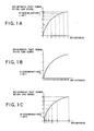
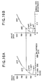
- the lateral axis represents brightness
- the vertical axis represents the brightness that human being can sense
- the human sense including visual sense can be represented substantially by Log characteristic.
- the steps of brightness which generate the difference of brightness that human being can discriminate are regular in interval when the brightness is represented by a Log scale (known as Waber-Fechner's law).
- the brightness corresponds linearly to drive data to be supplied into the modulation circuit (for example, when a simple pulse width modulation is performed, and the brightness realized by the display elements corresponds linearly to the pulse width), consideration can be made with the brightness shown in Fig. 1A with drive data.
- the brightness changes with drive data at steps that exceed the discrimination limit in the range of low brightness.
- the number of gradations is small in the range of low brightness.
- the brightness changes with drive data at steps below the discrimination limit, and hence human being cannot recognize that the brightness has changed. In other words, it is understood that useless drive data exists in the range of high brightness.
- Fig. 1B shows the brightness steps required for showing the gradation at such steps that human being does not recognize roughness of gradation (steps at the discrimination limit) when the gradation is shown with the brightness steps of regular intervals.
- the brightness steps require a large number of brightness steps (the total number of gradations in drive data) which is the brightness steps smaller than those shown in Fig. 1A.
- human being cannot recognize the change of brightness with one step.
- a method of non-linear driving as shown below (drive data and the brightness are not proportional) has been studied in order to achieve presentation of desirable gradation with the small total number of gradations in drive data.
- a non-linear driving method has been studied in which the brightness steps in each range of gradations are set so as to generate the difference in brightness which is equal to the discrimination limit. Consequently, the number of gradations in the range of high gradations is decreased while the number of gradations in the range of low gradations is increased.
- the brightness steps shown in the graph of Fig. 1C has a smaller total number of gradations in drive data in comparison with the case shown in Fig. 1B.
- human being perceives in the same manner as the case shown in Fig. 1B. Therefore, the high gradations can be realized with the small total number of gradations in drive data.
- improvement of gradation is achieved by a non-linear driving method in which the brightness steps in the range of low gradations which is a part of the area of all the gradations (the difference of brightness between the brightness obtained by a certain value in drive data and the brightness obtained by the value which is one bigger than the certain value in drive data) is set in smaller (on the normal scale) steps than the brightness steps in the area on the side higher in gradation with respect to the range of low gradations, not by a modulation method in which the brightness steps have regular intervals.
- improvement of gradation is achieved even with the same total number of gradations in drive data in comparison with the case in which the brightness steps are uniform in the range of all the gradations, suppression in lowering of gradation or improvement thereof when the total number of gradations in drive data is reduced is achieved, and when the total number of gradations in drive data is increased, improvement of gradation which is better than the effect achieved by such increase can be obtained.
- the first range of gradations is the lower range of gradations with respect to the second range of gradations and the second range of gradations is the higher range of gradations with respect to the first range of gradations.
- the first range of gradations is on the lower side of the second range of gradations and the brightness steps in the first range of gradations is set to the smaller steps than the brightness step in the second range of gradations is shown in the embodiment in this specification, it is not limited thereto, and may be set as needed.
- the previous stage of the modulation circuit is adapted to convert data having the larger total number of gradations than the total number of gradations in incoming drive data into the modulation circuit into data having the smaller total number of gradations.
- data to be corrected is preferably data proportional to the brightness (of linear characteristic).
- data proportional to the brightness (of linear characteristic) For example, it is studied and found that when performing signal processing on image data which is proportional to the brightness (of linear characteristic) for adjusting colors, calculating brightness data having a linear characteristic, and displaying it based on brightness data, the following configuration is suitable.
- the input value is a picture signal (gamma-corrected picture signal) on which correction is performed for achieving suitable display in CRT in advance, such as the TV signal
- the following construction is suitable. That is, improvement of gradations is proposed by;
- the converting process shown in (1) can be omitted when the incoming picture signal is not gamma-corrected.
- the object of signal processing is not limited to image data having the linear characteristic as long as it has such characteristic that signal processing can easily be performed.
- data having a predetermined characteristic may be converted into drive data corresponding to the brightness steps, such that the differences in brightness which human being senses are regular in interval.
- a favorable gradations which is not different from that displayed in the total number of gradations shown in (2) can be obtained by determining the drive conditions corresponding to the human sense as described above, and further by converting into drive data in which the total number of gradations is smaller than the total number of gradations in data on which processing with a linear characteristic is performed, which is performed in (2).
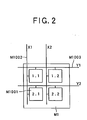
- Fig. 2 is a drawing showing a matrix panel including 2 rows ⁇ 2 columns for describing the basic operation.
- reference sign M1 designates a matrix panel
- reference sign M1001 designates a cold cathode element as a display element
- the cold cathode element M1001 is formed on a substrate, not shown.
- Reference sign M1002 designates a column wiring
- reference sign M1003 designates a row wiring. The intersections thereof are insulated, and the cold cathode elements M1001 are connected to the intersections of the row-and-column wiring.
- the cold cathode element M1001 is preferably a surface conducting electron emitting element.
- the matrix panel in Fig. 2 shows an example of monochrome display, which constitutes a display apparatus of 2 x 2 pixels.
- selected potentials are applied in sequence to the row wiring by the unit of horizontal synchronous signal of the incoming picture signal, and the column wiring is driven by a modulated signal corresponding to drive data of the selected row wiring, so that an image is formed.
- the selected potentials are applied in sequence during a selected period (1H: preferably, it is determined to the horizontal scanning period of the incoming picture signal).
- the selected period is a half the period of 1-frame of the incoming picture signal.
- a selected potential is applied to Y1 of the row wiring M1003 for the first half of the one-frame period of the incoming picture signal. Then, the modulated signal corresponding to the first scanning line is supplied to the column wiring M1002 (X1, X2) and an image of the first row is displayed. A selected potential is applied to Y2 of the row wiring M1003 for the latter half of the one-frame period of the incoming picture signal. Then, a modulated signal corresponding to the second scanning line is supplied to the column wiring M1002 (X1, X2), and the image of the second row is displayed. Consequently, a frame of image is displayed.
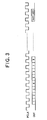
- a modulating method according to the first embodiment of the invention is a pulse width modification (PWM).
- the pulse width modulation enumerates a reference clock (referred to as PCLK), and outputs the pulses until becoming equal to the drive data of the corresponding column wiring.
- Fig. 3 shows the PCLK and a waveform of the modulated signal (OUT) from the pulse width modulator.
- numerals (1-1023) in rectangular boxes of the waveform of the modulated signal mean incoming drive data into the modulator. For example, when drive data is "5", the modulated signal is outputted until the time corresponding to the numeral "5" in the rectangular box, and no output is supplied from that time on.
- the rectangular boxes in the waveform of the modulated signal which represent gradations shown by numerals for convenience, are referred to as blocks or time slots. Since the crest value modulation is not used in the present embodiment, different from another embodiment described later, each time slot is constructed of one block.
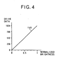
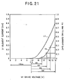
- Fig. 4 shows a characteristic of normalized brightness with respect to incoming drive data.
- the vertical axis represents incoming drive data of 10 bits in width
- the lateral axis represents the brightness. More accurately, although the brightness becomes discrete for discrete drive data, the characteristic is represented by a solid straight line.
- the brightness shows a characteristic which is proportional to period during which the modulated signal is applied to the cold cathode element M1001 (fd0).
- the driving method of the present embodiment has following features.
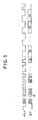
- Fig. 5 shows a waveform of a modulated signal according to the driving method of the invention.
- the waveform of the modulated signal (OUT) is shown together with the time slots.
- the cycle of PCLK is not constant, but variable.
- the cycle of PCLK is determined not for realizing the characteristic of the CRT, but for realizing the above-described gradation characteristic which improves the characteristic that human being can sense (to increase gradation) as described above.
- it is not such modulated signal that "the brightness steps are regular in interval", but is such modulated signal that the brightness steps are uneven in interval, more specifically, that the brightness steps in the range of low gradations is smaller than the brightness step in the range of high gradations.
- the cycle of PCLK is determined so that the modulated signal that can realize such brightness steps that "the differences sensed by human being are regular in interval" can be generated.
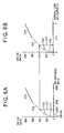
- Fig. 6B shows the characteristic of the normalized brightness with respect to incoming drive data.
- the vertical axis represents incoming drive data of 10 bits in width
- the lateral axis represents the brightness.
- the frequency of PCLK is selected so as to be the frequency of fPWM for drive data from “0" to "255”, half the frequency of fPWM for drive data from “256” to “383”, a quarter the frequency of fPWM for drive data from "384" to "767”, and eighth part of the frequency of fPWM for drive data from "768" to "1023".
- the brightness at this time is, as shown in Fig. 6B, since the frequency of PCLK is high in drive data from “0" to "255", increment of brightness is small with respect to drive data, and hence inclination in the graph is significant (straight line fd1).
- the characteristics of drive data from “255” to “383” can be represented by the straight line fd2, drive data from “383” to “767” by the straight line fd3, and drive data from "767” to "1023” by the straight line fd4, respectively.
- the gradation in the range of low gradations which is specially important for the visual characteristic of human being, can be increased to a gradation equal to the case in which modulation for equalizing the brightness steps is performed under much larger total number of gradations in data to be supplied into the modulation circuit, irrespective of the fact that the total number of gradations in data to be supplied into the modulation circuit is 1024. It is also effective even when the kinds of the frequencies of PCLK are reduced for simplifying the configuration of the hardware. It is further preferable to make the cycle of PCLK continuously variable by using a ROM or a VCO. Since the structure disclosed in JP-A-2000-29425 can be employed as a configuration of the actual hardware, the description will be omitted here.
- a significant characteristic of the present embodiment is that the driving conditions (PCLK cycle) can be determined so that the gradation that human being senses, particularly, in the range of low gradations is improved by converting brightness data having a desired characteristic, for example, the linear characteristic, into drive data.
- the desired characteristic means a characteristic preferable for an intended predetermined signal processing. For example, since the linear characteristic is preferable for color processing, this is recognized as the desired characteristic.
- a characteristic of the drive data converting unit for converting brightness data having, for example, the brightness-linear characteristic as the desired characteristic into drive data is shown in Fig. 6A.
- the lateral axis represents incoming brightness data of 12 bits in width
- the vertical axis represents converted drive data of 10 bits in width.
- conversion in the drive data converting unit is determined in such a manner that incoming data is converted into drive data, and brightness on which pulse width modulation is performed by drive data and displayed accordingly becomes proportional to brightness data.
- conversion is determined so that drive data falls within the range from “0” to “255” for brightness data in the range from “0” to “255” (straight line of ft1). It is determined so that drive data falls within the range from “255” to “383” for brightness data in the range from “255” to “511” (straight line of ft2). It is determined so that drive data falls within the range from “383” to “767” for brightness data in the range from “511” to "2047” (straight line of ft3). Then, it is determined so that drive data falls within the range from “767” to “1023” for brightness data in the range from “2047” to “4095” (straight line ft4).
- Brightness data "1024" is converted in the drive data converting unit that will be described later into drive data "512" (fp1).
- Drive data "512” is supplied into the pulse width modulator that will be described later, and a modulated signal that realizes the normalized brightness 0.25 is outputted (fp2). Therefore, brightness corresponding to brightness data can be obtained.
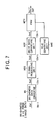
- Fig. 7 is an explanatory block diagram showing the basic configuration of the driving method according to the present embodiment.
- reference sign M4 designates a brightness data converter
- reference sign M20 designates a signal processing unit
- reference sign M30 designates a drive data converting unit
- reference sign M70 designates a pulse width modulator
- reference numeral M40 designates a PCLK generator.
- the brightness data converting unit M4 converts digital picture data (Sa1) which is gamma-converted, as the TV signal into image data (Sa2) having the linear characteristic. Signal processing such as color adjustment is performed on converted image data (Sa2) in the signal processing unit M20.
- the signal processing unit M20 outputs brightness data (Sa3) which is the result of performing signal processing.
- the drive data conversion unit M30 converts incoming brightness data (Sa3) into drive data (Sa4). In this conversion, conversion is performed in such a manner that the total number of gradations in outputted drive data (Sa4) is smaller than the total number of gradations in incoming brightness data (Sa3).
- the bit width of brightness data (Sa3) is determined to be 12 bits (4096 gradations), and the bit width of drive data is determined to be 10 bits (1024 gradations).
- the total number of gradations in data to be supplied into the pulse width converter M70 which constitutes the conversion circuit is 1024.
- signal processing is performed with data whose total number of gradations is 4096, which is larger than the above-described total number of gradations, as an input, and hence signal processing can be performed with a sufficient degree of accuracy.
- the total number of gradations for input is sufficient, processing of data corresponding to a predetermined image display element can be successfully performed even when it is performed depending on data corresponding to another image display element.
- high gradation is achieved with the small number of gradations of drive data as described above.
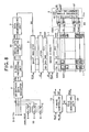
- a matrix image display panel 1 to be used in the image display apparatus according to the invention includes a multi-electron source formed by arranging a number of electron sources on a substrate in a low-profile vacuum container, for example, by arranging cold cathode elements 1001, and an image forming member such as a fluorescent material for forming an image by irradiation of electrons, opposing with respect to each other.
- the cold cathode elements 1001 as the display elements are disposed in the vicinities of the respective intersections of column wirings 1002 and row wirings 1003, and connected to both wirings. Since the cold cathode elements 1001 can be formed at accurate positions on the substrate by using the manufacturing technology such as photolithography etching, a number of elements can be arranged at minute intervals.
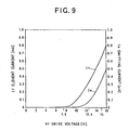
- the lateral axis represents the electron voltage Vf of the surface conducting emitting element, and the vertical axis represents examples of the element current If and the emitting current Ie.
- the threshold voltage about 7.5 V
- the emitting current Ie does not flow at a voltage below the threshold voltage.
- the emitting current Ie flows according to the element voltage applied. Utilizing this characteristic, the simple matrix drive shown below is preformed.
- reference numeral 1 designates the matrix image display panel including a multi-electron source formed of the cold cathode elements 1001 arranged on the substrate in the low-profile vacuum container.
- 480 elements that is, 160 pixels (RGB) ⁇ 3 are arranged horizontally, and for example, 240 elements are arranged in the vertical direction. While an example of the matrix image display panel having 480 pixels ⁇ 240 pixels is shown in the present embodiment, the number of elements is not limited thereto since it is determined by the application of the product as needed.
- the matrix image display panel 1 has a pixel arrangement of, for example, RGB stripes.
- Reference numeral 2 is an analogue-digital converter (A/D converter), for converting analogue RGB component signal (the name of the signal is referred to as SO) decoded for example from the NTSC signal to RGB signal by a decoder, not shown, into the digital RGB signals (S1) of 8 bits in width, respectively.
- A/D converter an analogue-digital converter
- Reference numeral 4 designates a brightness data converter (non-linear converting unit), and is a converting table to which the digital RGB signals (S1) from the A/D converter 2 or a computer are supplied and converted to have a desired brightness characteristic.
- a characteristic of the display system inverse conversion is performed on a signal which is gamma-corrected for the CRT for converting into a characteristic in which data is proportional to brightness (linear characteristic) (image data S2).
- This characteristic is preferably converted into such characteristic that can easily be processed in a signal processing unit 20 that will be described next.
- Reference numeral 20 is the signal processing unit (signal processing circuit), in which linear color conversion for performing, for example, color adjustment is performed to convert the color coordinate to be displayed.
- Reference numeral 30 designates a drive data converting unit, in which brightness data (S3) which is processed in the signal processing unit 20 is converted into drive data (S4).
- Reference numeral 3 is a data rearranging unit, which has a function to rearrange drive data (S4) for each color so as to meet the pixel arrangement of the matrix panel 1 and output (drive data S5).
- the data rearranging unit 3 is provided in the subsequent stage of the drive data converting unit 30 in Fig. 8, it is not limited thereto. It may be arranged upstream or downstream of the brightness data converter 4, the signal processing unit 20, and the drive data converting unit 30, or may be some location in between. In Fig. 8, since it is necessary to perform matrix calculation for each color when the signal processing unit 20 performs color processing or the like, the data rearranging unit 3 is provided in the subsequent stage of the drive data converting unit 30 to reduce the amount of hardware. While the portion for performing each function is illustrated in blocks in the drawings, it is not necessary to package each block independently, and a circuit that can perform the function of a plurality of blocks may be employed.
- Reference numeral 5 is a shift resistor for shift-transferring drive data S5 outputted from the drive data converting unit 30 in sequence by the shift clock (SCLK), and outputting drive data corresponding to the respective elements of the matrix panel 1 in parallel.
- Reference numeral 6 is a latch circuit for latching drive data from the shift resistor 5 in parallel by a load signal LD synchronized with a horizontal synchronous signal and holding it for a period until the next load signal LD is supplied.
- Reference numeral 7 is a drive circuit for enumerating the reference clock (PCLK) as described above, and driving the column wirings of the matrix panel 1 respectively at a pulse width according to incoming drive data.
- PCLK reference clock
- Reference numeral 8 designates a scan driver and is connected to the row wiring 1003 of the matrix panel 1.
- Reference numeral 81 is a scanning signal generating unit for shifting YST signal synchronized with a vertical synchronous signal of an incoming picture signal in sequence by a signal HD determined by a timing control unit 10, and outputting the selected/non-selected signals in parallel corresponding to the number of the row wirings.
- Reference numeral 82 is a switching means constructed of a MOS transistor or the like, which changes over the switch depending on the output level of the selected/non-selected signals from the scanning signal generating unit 81, and outputs selected potential (-Vss) and non-selected potential (GND).
- Reference numeral 10 is the timing control unit which outputs a synchronous signal of the incoming image and a control signal of a desired timing formed by the data sampling clock (DCLK) or the like to the respective function blocks.
- DCLK data sampling clock
- Reference numeral 40 is a PCLK generating unit as a clock supply circuit and outputs the PCLK whereof the cycle (frequency) varies as described above.
- the PCLK generating unit 4 may generate the clock, for example, by VCO or PLL, or may switch among a plurality of clocks and output the same.
- Fig. 10 is a timing chart showing the entire configuration of the image display apparatus.
- A/D converter 2 converts, for example, an analogue RGB component signal (SO) decoded from the NTSC signal to RGB signal by a decoder, not shown, into the digital RGB signal (S1) of, for example, 8 bits in width, respectively Thought it is not shown, it is preferably to generate a sampling clock (DCLK) by PLL based on the synchronous signal.
- SO an analogue RGB component signal
- S1 digital RGB signal
- DCLK sampling clock
- the brightness data converter 4 inputs a digital RGB signal (S1) which is picture data of A/D converter 2 or the computer.
- S1 digital RGB signal
- processing can be made easily when the number of data on one scanning line (1H) is determined by the number of pixels on the side of the column wirings on the matrix panel 1.
- the number of pixels on the side of the column wirings of the matrix panel 1 is determined to be 160.
- the digital RGB signal (S1) from the A/D converter 2 or the computer is outputted synchronously with the data sampling clock (DCLK), not shown.
- the brightness data converter 4 converts the digital RGB signal (S1), for example, from the A/D converter 2 or the computer into a characteristic in which, for example, the outgoing image data (S2) is proportional to the characteristic of brightness using a conversion table (ROM), not shown, in which a desired data is stored (linear characteristic) in advance.
- the brightness referred here means the brightness of the incoming signal source.
- the brightness data converter 4 can convert into image data of 12 bits in width having a linear characteristic by performing inversed gamma-conversion by the power of 2.2.
- signal processing is performed for the characteristics other than the linear characteristic as described above, it is preferable to convert it into the characteristic, which is required by the processing.
- FIG. 11 An example of a characteristic of the conversion table for converting into a linear characteristic is shown in Fig. 11.
- Image data (S2) of 12 bits in width that the brightness data converter 4 outputs is supplied into the signal processing unit 20.
- the signal processing unit 20 performs a linear color conversion, for example, for color adjustment, and converts the color coordinate to be displayed. More specifically, image data (S2) in each color is converted by a matrix calculating unit of 3 rows, 3 columns. Then, converted brightness data (S3) is outputted.
- the signal processing unit 20 is not limited to color adjustment, but is suitable for signal processing for correcting voltage drop of the row wirings on the matrix panel, which is disclosed in JP-A-08-248920 according to the invention of the present applicant.
- Brightness data (S3) outputted from the signal processing unit 20 is supplied into the drive data conversing unit 30.
- the drive data converting unit 30 converts incoming brightness data (S3) of 12 bits in width having a linear characteristic into drive data (S4) of 10 bits in width in which the displayed brightness characteristic of the matrix panel becomes linear with respect to the brightness data (S3) as described above. More specifically, it is preferable to realize using a ROM table having a characteristic described later.
- the signal processing unit 20 and the drive data converting unit 30 realize a function to perform signal processing on incoming data (data having the total number of gradations, which is the total number of gradations suitable for signal processing, and larger than the total number of gradations in data to be supplied into the conversion circuit) and reduced the total number of gradations so as to meet the total number of gradations supplied into the conversion circuit.
- the data rearranging unit 3 has a function to rearrange drive data (S4) for each color so as to meet the pixel arrangement on the matrix panel 1 and output it (drive data S5).
- the signals (drive data S4) supplied into the data rearranging unit 3 are switched at a timing of the shift clock (SCLK) having a frequency as much as three times the data sampling clock (DCLK), and are outputted in sequence from the output terminal of the data rearranging unit 3 (S5) according to the RGB pixel arrangement on the matrix panel 1.
- SCLK shift clock
- DCLK data sampling clock
- the data rearranging unit 3 sends the output signals (S5) to the shift resister 5 of 10 bits in width and shift-transfers in sequence according to the shift clock (SCLK), and then performs serial-parallel conversion on drive data corresponding to each element on the matrix panel 1, and outputs it. Then, the latch 6 latches drive data having been serial-parallel converted when the load signal LD which is synchronized with the horizontal synchronous signal is rising and holds data until the next load signal LD is supplied.
- SCLK shift clock
- the drive circuit 7 drives the column wirings (X1-X480) synchronously with the PCLK based on the time of the load signal LD in a manner described above.
- the scan driver 8 transfers signals (YST) for determining the scan start time in sequence synchronously with the horizontal synchronous signals (HD) to drive the row wiring as shown in Fig. 10. Then, it scans the row wirings in sequence and forms an image.
- the scan driver 8 drives the row wirings from the first (Y1) to the 240th (Y240) in sequence at a selected voltage -Vss (for example, -7.5 V) synchronously with HD. In this case, the scan driver 8 drives the voltage of other row wirings, which are not selected, to the non-selected voltage, 0V.
- a selected voltage -Vss for example, -7.5 V
- the scan driver 8 drives the row wirings from the first to the 240th in sequence synchronously with the HD at the selected voltage, and the drive circuit 7 drives the corresponding row wirings with the modulated signal S17 corresponding to drive data to form a image.
- the invention can be applied to a scanning system in which the scan driver 8 selects two or more row wirings simultaneously to improve the brightness.
- NTSC signal display on the matrix image display panel 1 having 240 scanning wirings 480 scanning wirings out of 485 interlaced effective scanning wirings were overwritten and driven on the matrix image display panel 1 every field.
- One field of NTSC signal was treated as one frame on the matrix image display panel 1.
- the matrix image display panel 1 was driven as a picture signal with frame frequency of 60Hz and 240 scanning lines.
- duration required for displaying one scan line was about 63.5 ⁇ sec for NTSC signal, and about 56.5 ⁇ sec within this specific duration was determined to be the maximum duration for the drive pulse for the column wirings. Therefore, since the PCLK selected the time slot 1023 for the maximum drive pulse width, a frequency, at which about 56.5 ⁇ sec can be achieved when the number of pulses of PCLK is 1023, was selected.
- the frequency of PCLK was determined as described above. In other words, the characteristic shown in Fig. 6B is achieved.
- the vertical axis represents incoming drive data
- the lateral axis represents the brightness.
- the frequency of PCLK is determined to 72.48 MHz for drive data from “0” to “255”, to 36.24 MHz for drive data from “256” to “383”, to 18.12 MHz for drive data from "384" to "767”, and to 9.06 MHz for drive data from "768" to "1023".
- the brightness at this time is, as shown in Fig. 6B, since the frequency of PCLK is high in drive data from “0" to "255", increment of brightness is small with respect to drive data, and hence inclination in the graph is significant (straight line fd1).
- the characteristics of drive data from “255” to “383” is represented by the straight line fd2, drive data from “383” to “767” by the straight line fd3, and drive data from "767” to "1023” by the straight line fd4, respectively.
- the characteristic of the drive data converting unit 30 is the characteristic of the above-described Fig. 6B.
- characteristic of the drive data converting unit 30 is determined so that drive data falls within the range from “0" to "255” for brightness data in the range from “0” to “255” (straight line of ft1), within the range from “255” to “383” for brightness data in the range from “255” to “511” (straight line of ft2), within the range from “383” to “767” for brightness data in the range from “511” to "2047” (straight line of ft3), and within the range from "767” to "1023” for brightness data in the range from “2047” to “4095” (straight line ft4).
- the number of gradations corresponding to 12 bits, 11 bits, 10 bits, and 9 bits in brightness data conversion of the linear characteristic from the low brightness on is realized.
- the scan driver 8 drives the row wirings from the first (Y1) to the 240th (Y240) in sequence at a selected voltage -Vss (for example, -7.5 V) synchronously with the horizontal synchronous signal HD. In this case, the scan driver 8 drives the voltage of other row wirings, which are not selected, to the non-selected voltage, 0V.
- voltages to be applied to the column wirings are represented by VX1, VX2 ...
- voltages to be applied to the row wirings are represented by VY1, VY2, VY3 ....
- the scan driver 8 has to maintain the rows to be selected at a selected voltage for the maximum duration (time slots 1 to 1023) for the drive pulse width.
- the drive circuit 7 which performs the pulse width modulation with drive data of 10 bits in width can achieve display with brightness resolution corresponding to the 12 bits gradation having a linear characteristic in the range of low brightness.
- a high gradation is achieved with the small number of brightness steps utilizing the characteristic of the human sense.
- a characteristic corresponding to the pulse width modulation of about 12 bits can be obtained with the 10 bits pulse width modulator.
- manufacturing cost for the drive circuit, especially the modulation circuit is high. Therefore, the invention in which a high gradation can be achieved with the small number of drive data width (the bit width of the modulator can be reduced even with the total number of gradations which is recognized as the same) is suitable for cost reduction of the image forming apparatus.
- display at preferable gradation is achieved even when signal processing for color adjustment or signal processing for correcting the effect of voltage drop in the row wirings are performed.
- a second embodiment of the invention will be described.
- the basic operation of the driving method according to the second embodiment of the invention will be described.
- the basic operation will be described referring to the matrix panel shown in Fig. 2. Description of the components and the general driving method in Fig. 2 are omitted.
- the method of modulating according to the second embodiment of the invention is a modulating method in which the pulse width modulation (PWM) and the crest value modulation are combined.
- PWM pulse width modulation
- crest value modulation amplitude modulation
- a crest value modulation preference type combined modulation which is a method in which the crest value modulation is performed in preference to the pulse width modulation.
- pulse width modulation preference type combined modulation as a method of performing the pulse width modulation in preference to the crest value modulation. This method is performed by increasing the pulse width according to increase in drive data in a state in which the crest value is set to a predetermined value, and when all the pulse widths available are used completely, increasing the crest value for the larger drive data, and increasing the pulse width for the portion of the increased crest value according to increase in drive data.
- a predetermined condition may be set to the available range of crest values or the available range of pulse width.
- a condition for limiting the available range of crest values so as to control abrupt change in crest value at the point where the crest value of the modulated signal changes.
- the available range of crest values is set to a smaller value than the crest value that the modulation circuit can output as a crest value of the modulated signal at the rising portion and/or the falling portion of the modulated signal, so that the rising and/or falling portion of the waveform of the modulated signal maintains a stepped shape without setting all the crest values in the range that the modulation circuit can output as the crest value of the modulated value as the available range of crest values
- the rising and/or falling portion of the waveform of the modulated signal maintains a stepped shape without setting all the crest values in the range that the modulation circuit can output as the crest value of the modulated value as the available range of crest values.
- a condition to limit the available range of pulse widths can be set so as to control the abrupt change in crest value at the point where the crest value of the modulated signal changes. More specifically, such condition that the range of pulse widths available in the predetermined crest value is set to a value smaller than the range of pulse widths available in the crest value smaller than the predetermined crest value so that the rising and/or falling portion of the waveform of the modulated signal has a stepped shape without setting the range of the pulse widths available in each crest value to the same range can be preferably employed.
- An example of setting of these conditions is disclosed in WO/1267319.
- the modulating method according to the second embodiment employs the crest value modulation preference type combined modulation.
- the configuration in which the brightness steps are varied by varying increment in pulse width of the modulated signal can be preferably employed.
- the configuration in which the cycle of the reference clock (PCLK; a clock to be enumerated for determining the pulse width) is made to be uneven as in the first embodiment can be employed as a configuration to make increment of the pulse width of the modulated signal uneven.
- PCLK reference clock
- the above-described condition that the rising and falling portions of the modulated signal take a stepped shape is employed.
- An example of the waveform of the outgoing modulated signal is shown in Fig. 12.
- Fig. 12 shows the PCLK and the waveform.of the modulated signal (OUT).
- the numerals (1-1023) in the rectangular box of the waveform of the modulated signal means drive data, and when drive data is, for example, "12", the waveform of the modulated signal is those having numerals smaller than "12" in the rectangular box.
- the rectangular box showing gradations is referred also to as block for convenience.
- the time width which is a unit of control of the pulse width is referred to as a time slot.
- the crest value of each slot is determined synchronously with the rising waveform of PCLK, which is the reference clock.
- the time slot having the crest value of any one of V2, V3, and V4 includes a plurality of blocks. However, it is not necessarily required to output the plurality of blocks independently.
- Such control of waveform of the modulated signal is crest value control including pulse width control for each slot width, which is determined corresponding to the frequency of the reference clock, and crest value control for each slot width.
- the present embodiment employs a condition in which the waveform of the signal takes a stepped shape at the rising and falling portions of the modulated signal. This condition can be said as follows.
- crest value control is performed on the crest value in each slot at least in n-stages from A1 to An (where n is an integer number of two or larger and 0 ⁇ A1 ⁇ A2 ⁇ ...An), and has a rising portion passing via the respective crest values from A1 to Ak-1 at least one slot each in sequence to a predetermined crest value Ak (where k is an integer number between 2 and n inclusive), and a falling portion passing via the respective crest values from Ak-1 to A1 at least one slot each in sequence beginning with the predetermined crest value Ak.
- the modulated signal has a voltage waveform, and the voltage is composed of the crest values of four stages from V1 to V4.
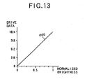
- Fig. 13 shows a characteristic of normalized brightness with respect to incoming drive data in dots.
- the vertical axis represents incoming drive data of 10 bits in width
- the lateral axis represents the brightness. More accurately, although the brightness becomes discrete for discrete drive data, the characteristic is represented by a solid straight line.
- the crest value that the modulation circuit can output is GND, which is the reference potential corresponding to the OFF state and four crest values V1, V2, V3, and V4 which correspond to the respective different ON-states.
- these crest values are set in such a manner that, as a result of increment of drive data by one from a certain value, increment in brightness (brightness steps) when the crest value of the slot of a predetermined width is increased from GND to V1, increment in brightness (brightness steps) when the crest value of the slot of the predetermined width is increased from V1 to V2, increment in brightness (brightness steps) when the crest value of the slot of the predetermined width is increased from V2 to V3, and increment in brightness (brightness steps) when the crest value of the slot of the predetermined width is increased from V3 to V4 as drive data increases one from a certain value are equal with respect to each other.
- the differential of the crest value is set in such a manner that the brightness steps are regular in interval with respect to drive data.
- diversification of the intervals of the brightness steps in the present embodiment is performed by diversification of the intervals of increment in pulse width as in the first embodiment.
- FIG. 14 A characteristic and each voltage of the surface conducting electron emitting element used in the invention are shown in Fig. 14. Assuming that there is no saturation of fluorescent material, the intervals of the emitting current Ie (that is, brightness) determined by V1, V2, V3, and V4 as shown in Fig. 14 may be set to be equalized. It is also preferable to measure the brightness and set the values of V1, V2, V3, and V4.
- V1, V2, V3, and V4 are employed as the modulation reference voltages, any configuration may be applied to the second embodiment of the invention as long as the crest values corresponding to at least two ON-states which are different from each other are employed.
- the configuration of voltage drive in which the potential is set to a predetermined value is disclosed as the crest value, it is not limited thereto.
- the driving method of the second embodiment is the same as the first driving method.
- Fig. 2 Detailed description of Fig. 2 is omitted since it is already described in conjunction with the first embodiment.
- high gradation is achieved by the limited total number of gradations in drive data as in the first embodiment by varying the cycle of PCLK and making the characteristic of the brightness corresponding to drive data non-linear as in the first embodiment.
- the waveform of the modulated signal (OUT) is shown with the slots.
- the cycle of PCLK is varied.
- the above-described gradation characteristic for achieving preferable characteristic that human being can sense (to achieve high gradation) is realized.
- the brightness steps are set to be "brightness that human being can sense are regular in interval” but not "brightness step of regular intervals".
- FIG. 16B A characteristic of normalized brightness with respect to incoming drive data will be shown in Fig. 16B.
- the vertical axis represents incoming drive data of 10 bits in width
- the lateral axis represents the brightness.
- the frequencies of PCLK is selected in such a manner that the cycle of fPWM is selected for the number of PCLK from “1" to “67”, half the frequency of fPWM is selected for the number of PCLK from “68” to “129”, a quarter the frequency of fPWM is selected for the number of PCLK from “130” to "225”, and eight part the frequency of fPWM is selected to the number of PCLK from "226" to "258".
- Fig. 17 is a drawing for providing easy comprehension of increment in brightness with respect to increment in drive data.
- the vertical axis represents incoming drive data
- the lateral axis represents the brightness.
- An enlarged drawing near the drive data "256" is shown. It will be seen that increment in brightness actually varies in erratic pattern with respect to increment in drive data.
- a characteristic of the drive data converting unit that will be described later is preferably be determined while taking the characteristic shown in Fig. 17 into account.
- the characteristic which is substantially similar to the visual characteristic of human being is achieved. It is also effective to reduce the sorts of frequencies of PCLK for simplifying the hardware configuration as a matter of course. It is further preferable to make the cycle of PCLK continuously variable by the use of ROM or VCO. Since the configuration disclosed in JP-A-2000-29425 can be employed as an actual hardware configuration for realizing the PCLK of uneven cycle, description will be omitted here.
- This embodiment is also characterized in that brightness data having a desirable characteristic, for example, a linear characteristic, is converted into drive data, and the driving conditions (cycle of PCLK) are determined so as to improve gradation in the range of low gradations.
- a desirable characteristic for example, a linear characteristic
- the driving conditions cycle of PCLK
- the desirable characteristic is the linear characteristic in the case of color processing.
- a characteristic of the drive data converting unit for converting brightness data having, for example, the brightness-linear characteristic as the desirable characteristic into drive data is shown in Fig. 16A.
- the lateral axis represents incoming brightness data of 12 bits in width
- the vertical axis represents converted drive data of 10 bits in width. Since incoming brightness data has a linear characteristic (data indicating the brightness that the value of data should indicate), in Fig. 16A, the characteristic of the drive data converting unit is determined in such a manner that incoming brightness data is converted into drive data, and further, brightness modulated by drive data and then displayed is accordingly proportional to brightness data.
- conversion is determined so that drive data falls within the range from “0” to “255” for brightness data in the range from “0” to “255” (straight line of gt1). It is determined so that drive data falls within the range from “255” to “383” for brightness data in the range from “255” to “511” (straight line of gt2). It is determined so that drive data falls within the range from “383” to “767” for'brightness data in the range from “511” to "2047” (straight line of gt3). Then, it is determined so that drive data falls within the range from “767” to “1023” for brightness data in the range from “2047” to “4095” (straight line gt4).
- the table is set so that the value in which variations described above are corrected are outputted in the vicinity of the inflection point of the characteristic of the drive data converting unit.
- Brightness data "1024" is converted in the drive data converting unit into drive data "512" (gp1).
- Drive data "512” is supplied into the width modulator, and the normalized brightness 0.25 is outputted (gp2). Therefore, brightness corresponding to brightness data can be obtained.
- Fig. 16A and Fig. 16B even with the modulation of drive data of 10 bits gradation, the number of gradations corresponding to 12 bits, 11 bits, 10 bits, and 9 bits in brightness data conversion of the linear characteristic from the low brightness in sequence is realized.
- Fig. 18 is an explanatory block diagram showing the basic configuration of the driving method according to the present embodiment.
- reference sign M71 designates a modulator which is for supplying the modulation reference voltages GND, V1, V2, V3, and V4 and outputs the modulated signals described above. Since other configurations are the same as those in the first embodiment, description will be omitted.
- the brightness data converter M4 converts digital picture data (Sa1) which is gamma-converted, as the TV signal, and then into image data (Sa2) having the linear characteristic. Signal processing such as color adjustment is performed on converted image data (Sa2) in the signal processing unit M20.
- the signal processing unit M20 outputs brightness data (Sa3) which is the result of performing signal processing.
- the drive data converting unit M30 converts incoming brightness data (Sa3) into drive data (Sa4). In this conversion, conversion is performed in such a manner that the total number of gradations in outputted drive data (Sa4) is smaller than the total number of gradations in incoming brightness data (Sa3).
- the bit width of brightness data (Sa3) is determined to be 12 bits (4096 gradations), and the bit width of drive data is determined to be 10 bits (1024 gradations).
- the drive circuit 7 which performs the modulation with drive data of 10 bits in width can achieve display with brightness resolution corresponding to the 12 bits gradation having a linear characteristic in the range of low brightness.
- a high gradation is achieved with the small number of brightness steps utilizing the characteristic of the human sense.
- a characteristic corresponding to the modulation of about 12 bits in width can be obtained with the 10-bit width modulator.
- manufacturing cost for the drive circuit, especially the modulation circuit is high, and hence the invention in which a high gradation can be achieved with the small number of drive data width (the bit width of the modulator can be reduced even with the total number of gradations which is recognized as the same) is suitable for cost reduction.
- the method of the invention can cope with signal processing of color adjustment or signal processing for correcting the effect of voltage drop in the row wirings.
- a third embodiment of the invention will be described.
- the basic operation of the driving method according to the third embodiment of the invention will be described.
- the basic operation will be described referring to the matrix panel shown in Fig. 2. Description of the components in Fig. 2 and the general driving method are omitted.
- a modulating method different from the first embodiment and the second embodiment is employed.
- a method of modulating the column wirings will be described.
- the method of modulating according to the third embodiment of the invention is a modulating method in which the pulse width modulation (PWM) and the crest value modulation are combined as in the second embodiment.
- PWM pulse width modulation
- the third embodiment employs a pulse width modulation preference type combined modulation.
- FIG. 19A An example of the waveform of an outgoing modulated signal is shown in Fig. 19A.
- Fig. 19A shows the PCLK and the waveform of the modulated signal (OUT).
- the numerals (1-1024) in the rectangular box of the waveform of the signal means drive data, and when drive data is, for example, "9", the waveform of the modulated signal is those having numerals smaller than "9" in the rectangular box.
- the rectangular box is referred also to as block for convenience.
- the crest value of each slot is determined synchronously with the rising waveform of PCLK, which is the reference clock.
- Control of such modulated signal can be expressed as such control that enumeration is performed by the reference clock and pulse width control is performed by the unit of slot width ⁇ t based on the enumerated value and drive data, crest value control is performed on the crest value at each slot at least in n-stages from A1 to An (where n is an integer number equal to or larger than two, and 0 ⁇ A1 ⁇ A2 ... An), and the waveform which is increased in gradation with respect to the predetermined waveform of the modulated signal has such shape that a unit waveform block which is determined by the slot width and the crest value An-An-1,...
- the modulated signal is a voltage waveform, and the voltage is composed of crest values of four stages from V1 to V4.
- Fig. 20 shows an example of the characteristic of normalized brightness with respect to incoming drive data.
- the vertical axis represents incoming drive data
- the lateral axis represents the brightness. More accurately, although the brightness becomes discrete for discrete drive data, the characteristic is represented by a solid straight line (hd0).
- Shown in Fig. 20 is an example in which a linear characteristic is achieved by selecting a'voltage (modulation reference voltage: GND, V1, V2, V3, and V4).
- a linear characteristic is achieved.
- these crest values are set by differentiating increment in brightness (brightness steps) when the crest value of the slot of a predetermined width is increased from GND to V1, increment in brightness (brightness steps) when the crest value of the slot of the predetermined width is increased from V1 to V2, increment in brightness (brightness steps) when the crest value of the slot of the predetermined width is increased from V2 to V3, and increment in brightness (brightness steps) when the crest value of the predetermined width is increased from V3 to V4 as drive data increases one from a certain value, not by equalizing these increments.
- the brightness steps at a crest value corresponding to the range of low gradations which requires visually small brightness steps in terms of visual sense of human being, is set to be small. More specifically, the brightness steps at the crest value V1 corresponding to the range of low gradations is set to be smaller than the brightness steps in the crest value V4 corresponding to the range of high gradations.
- FIG. 21 A characteristic and each voltage of the surface conducting electron emitting element used in the third embodiment of the invention are shown in Fig. 21. Assuming that there is no saturation of fluorescent material, the intervals of the emitting current Ie (that is, brightness) determined by V1, V2, V3, and V4 as shown in Fig. 21 are selected as:
- Fig. 22B shows a characteristic of the normalized brightness with respect to incoming drive data. It was also preferable when the brightness was measured and V1, V2, V3, and V4 are set to achieve a desired characteristic.
- any configuration may be applied to the third embodiment of the invention as long as the crest values corresponding to at least two ON-states which are different from each other are employed.
- a high gradation is achieved when the modulation reference voltage is selected so as to achieve a resolution of low gradation.
- the obtained curve of the characteristic has an effect to improve the gradations also in cases other than that shown in the present embodiment.
- the cycle of PCLK is not varied unlike the case of the first and the second embodiments. Therefore, it is a method in which a problem such as the limit of the operational frequency of the semiconductor due to increase in frequency of PCLK can hardly occur.
- the third embodiment by determining the modulation reference voltages GND, V1, V2, V3, and V4 as described above, the non-linear characteristic of the brightness corresponding to drive data is achieved, and a high gradation is achieved by the limited total number of gradations in drive data as in the first and second embodiments.
- the value of the modulation reference voltages GND, V1, V2, V3, and V4 are varied from the linear characteristic. Then, the gradation characteristic for achieving desirable characteristic that human being can sense (for achieving the high gradation) as described above. That is, the "brightness step of regular intervals" is changed to such brightness step that "the differences in brightness that human being can sense are regular in interval".
- Fig. 22B shows a characteristic of the normalized brightness with respect to the incoming drive data.
- the vertical axis represents incoming drive data
- the lateral axis represents the brightness.
- the brightness at that time is, as shown in Fig. 22B, small in increment with respect to the drive data and hence inclination on the graph is significant (straight line hd1) for drive data from "0" to "256".
- the characteristics of drive data from “256” to "512” is represented by the straight line hd2, drive data from “512” to “768” by the straight line hd3, and drive data from "768" to "1024" by the straight line hd4.
- This embodiment is characterized in that brightness data of the desired characteristic, for example, of the linear characteristic is converted into drive data, and the driving conditions (modulation reference voltages GND, V1, V2, V3, and V4) are determined so that the intervals of brightness that human being senses with respect to drive data becomes closer to the regular interval.
- the desired characteristic for color processing is the linear characteristic.
- a characteristic of the drive data converting unit for converting brightness data having, for example, the brightness-linear characteristic as the desired characteristic into drive data is shown in Fig. 22A.
- the lateral axis represents incoming brightness data of 12 bits in width
- the vertical axis represents converted drive data. Since incoming brightness data has a linear characteristic here, in Fig. 22A, the characteristic of the drive data converting unit is determined in such a manner that incoming brightness data is converted into drive data, and further, the brightness modulated by drive data and then displayed is accordingly proportional to brightness data.
- conversion is determined so that drive data falls within the range from “0” to “256” for brightness data in the range from “0” to “256” (straight line of ht1). It is determined so that drive data falls within the range from “257” to “512” for brightness data in the range from “257” to "1024" (straight line of ht2).
- Brightness data "1024" is converted in the drive data converting unit into drive data "512" (hp1).
- Drive data "512” is supplied into the pulse width modulator, and the normalized brightness 0.25 is outputted (hp2). Therefore, brightness corresponding to brightness data can be obtained.
- Fig. 22A and Fig. 22B even with the modulation of drive data of 10 bits in width, equivalent to the number of gradations corresponding in sequence to 12 bits, 11 bits, 10 bits, and 9 bits in brightness data conversion of the linear characteristic from the low brightness on is realized as in the first and second embodiments.
- Fig. 23 is an explanatory block diagram showing the basic configuration of the driving method according to the invention.
- reference sign M72 designates a modulator, which is for supplying the modulation reference voltages: GND, V1, V2, V3, and V4 and outputs the modulated signals described above.
- Reference sign M41 designates a CLK generating unit, and in the third embodiment, the PCLK of a fixed frequency is generated. Since other components are the same as the first embodiment, description will be omitted.
- the brightness data converter M4 converts digital picture data (Sa1) which is gamma-converted, as the TV signal, and then into image data (Sa2) having the linear characteristic. Signal processing such as color adjustment is performed on converted image data (Sa2) in the signal processing unit M20.
- the signal processing unit M20 outputs brightness data (Sa3) having a linear characteristic which is the result of performing signal processing.
- the drive data converting unit M30 converts incoming brightness data (Sa3) into drive data (Sa4). In this conversion, conversion is performed in such a manner that the total number of gradations in outputted drive data (Sa4) is smaller than the total number of gradations in incoming brightness data (Sa3).
- the bit width of brightness data (Sa3) is determined to be 12 bits (4096 gradations), and the bit width of drive data is determined to be 10 bits (1024 gradations).
- Fig. 19B shows another example of the modulating method according to the third embodiment.
- the pulse width modulation preference type combined modulation is employed, in which the reference clock (referred to as PCLK) is enumerated and the pulse width and the crest value corresponding to drive data are determined.
- PCLK reference clock
- This method is a modulating method in which the waveform of the modulating signal is extended in the direction of time, and when it cannot be extended anymore, the waveform is widened in the direction of crest value.
- the rising and falling waveforms of the modulated signal are controlled to be a stepped shape in order to reduce ringing of the drive waveform in the matrix panel.
- such waveform control of the modulated signal can be said to be control in which the waveform further increased by one gradation by adding the unit waveform block to the waveform with the maximum crest value Ak and having the number of slots of S-2(k-1), where the maximum number of slots is S, can be controlled to be a waveform having such shape that the crest value of the given slot out of the k+1 st to the S-k th slots is changed from Ak to Ak+1.
- the value S is 259.
- such condition that the range of pulse widths available in the predetermined crest value is set to a value smaller than the range of pulse widths available in the crest value smaller than the predetermined crest value so that the rising and/or falling portion of the waveform of the modulated signal has a stepped shape without setting the range of the pulse widths available in each crest value to the same range can be preferably employed.
- the modulation reference values: GND, V1, V2, V3, and V4 are set.
- brightness data is set to 12 bits in width
- drive data is set to 10 bits in width. Then drive data is determined to fall within the range from “0" to "259” for brightness data from “0" to “259". That is, the proportion of brightness data and drive data are set to 1:1. Drive data is determined to fall within the range from “260" to "516” for the brightness data from “260" to "1030". In other words, "259” is subtracted from the brightness data, and then divided by 3, added by “259” to obtain drive data. Drive data is determined to fall within the range from “517” to "771" for brightness data "1031" to "2050".
- the modulation reference voltages of: GND, V1, V2, V3, and V4 are preferably set at a normalized brightness, as follows. when drive data is “259”, 259/4096, when drive data is “516”, 1030/4096 when drive data is “771”, 2050/4096 when drive data is 1023, 4095/4096
- the drive circuit 7 which performs the modulation with data of 10 bits in width can achieve display with brightness resolution corresponding to the 12 bits gradation having a linear characteristic in the range of low brightness.
- a high gradation is achieved with the small number of brightness steps utilizing the characteristic of the human sense.
- a characteristic corresponding to the pulse width modulation of about 12 bits can be obtained with the 10 bits width modulator.
- manufacturing cost for the drive circuit, especially the modulation circuit is high, and hence the invention in which a high gradation can be achieved with the small number of drive data width (the bit width of the modulator can be reduced even with the total number of gradations which is recognized as the same) is suitable for cost reduction.
- the method of the invention can cope with signal processing of color adjustment or signal processing for correcting the effect of voltage drop in the row wirings.
- the invention is characterized in that display recognized as a high gradation is achieved with the small total number of graduations in drive data utilizing the human sense by changing the driving conditions (PCLK, modulation reference voltage) so as to achieve the non-linear brightness with respect to incoming drive data into the modulator.
- display to be recognized as a high gradation is achieved by the small total number of gradations in drive data utilizing the characteristic of the human sense by changing the driving conditions (PCLK, modulation reference voltage), and hence changing driving energy (driving amount) to be supplied to the display elements to achieve the non-linear brightness with respect to incoming drive data into the modulator. Therefore, the invention can be applied to other modulating method to bring about the effect.
- brightness data which is the desired characteristics (in particular, linear characteristic) is converted into drive data by the drive data converting unit to achieve the desired characteristics (in particular, linear characteristic) between brightness data and the brightness.
- the total number of gradations in drive data can be reduced by the total number of gradation in brightness data.
- Linear brightness data is preferable for signal processing such as color adjustment, and in the invention in which the bit width is increased, calculation with high degree of accuracy is enabled.
- signal processing may be other types of processing.
- the cold cathode electron emitting elements in the invention has been described, other various electron emitting elements such as the surface conducting emitting element, FE type emitting element, or MIM type emitting element can be used.
- various image display elements such as EL element which performs simple matrix drive can also be employed.
- Driving condition is determined so that the stimulating values of brightness with respect to drive data become closer to being regular in interval.
- the frequency of a reference clock used for the pulse width modulation is changed to be higher than the range of high gradations in the range of low gradations in drive data. Accordingly, smaller increment in brightness in the range of low gradation and larger increment in the range of high gradations are achieved.
Landscapes
- Engineering & Computer Science (AREA)
- Physics & Mathematics (AREA)
- Computer Hardware Design (AREA)
- General Physics & Mathematics (AREA)
- Theoretical Computer Science (AREA)
- Multimedia (AREA)
- Control Of Indicators Other Than Cathode Ray Tubes (AREA)
- Transforming Electric Information Into Light Information (AREA)
- Liquid Crystal Display Device Control (AREA)
- Liquid Crystal (AREA)
Applications Claiming Priority (2)
| Application Number | Priority Date | Filing Date | Title |
|---|---|---|---|
| JP2003141090 | 2003-05-19 | ||
| JP2003141090A JP4012118B2 (ja) | 2003-05-19 | 2003-05-19 | 画像表示装置 |
Publications (2)
| Publication Number | Publication Date |
|---|---|
| EP1480191A2 true EP1480191A2 (de) | 2004-11-24 |
| EP1480191A3 EP1480191A3 (de) | 2007-11-28 |
Family
ID=33095396
Family Applications (1)
| Application Number | Title | Priority Date | Filing Date |
|---|---|---|---|
| EP04011829A Withdrawn EP1480191A3 (de) | 2003-05-19 | 2004-05-18 | Bildanzeigegerät |
Country Status (5)
| Country | Link |
|---|---|
| US (1) | US7423661B2 (de) |
| EP (1) | EP1480191A3 (de) |
| JP (1) | JP4012118B2 (de) |
| KR (1) | KR100594679B1 (de) |
| CN (1) | CN100377184C (de) |
Cited By (1)
| Publication number | Priority date | Publication date | Assignee | Title |
|---|---|---|---|---|
| EP1833038A1 (de) * | 2006-03-09 | 2007-09-12 | Samsung SDI Co., Ltd. | Flachbildschirmgerät und Verfahren zur Erzeugung von Datensignalen dafür |
Families Citing this family (27)
| Publication number | Priority date | Publication date | Assignee | Title |
|---|---|---|---|---|
| US7669134B1 (en) | 2003-05-02 | 2010-02-23 | Apple Inc. | Method and apparatus for displaying information during an instant messaging session |
| JP2005260849A (ja) * | 2004-03-15 | 2005-09-22 | Toshiba Corp | 表示装置と表示方法 |
| JP4494298B2 (ja) * | 2005-06-24 | 2010-06-30 | シャープ株式会社 | 駆動回路 |
| JP4630752B2 (ja) * | 2005-07-29 | 2011-02-09 | 株式会社東芝 | 映像信号処理装置及び映像信号処理方法 |
| US7471442B2 (en) * | 2006-06-15 | 2008-12-30 | Qualcomm Mems Technologies, Inc. | Method and apparatus for low range bit depth enhancements for MEMS display architectures |
| US9304675B2 (en) | 2006-09-06 | 2016-04-05 | Apple Inc. | Portable electronic device for instant messaging |
| JP4926679B2 (ja) * | 2006-12-06 | 2012-05-09 | キヤノン株式会社 | 画像表示装置 |
| US8085282B2 (en) * | 2006-12-13 | 2011-12-27 | Canon Kabushiki Kaisha | Image display apparatus and driving method of image display apparatus |
| JP5034646B2 (ja) | 2007-04-20 | 2012-09-26 | 富士通株式会社 | 液晶表示素子及びその駆動方法並びにそれを備えた電子ペーパー |
| US9954996B2 (en) | 2007-06-28 | 2018-04-24 | Apple Inc. | Portable electronic device with conversation management for incoming instant messages |
| JP4627773B2 (ja) * | 2007-10-16 | 2011-02-09 | Okiセミコンダクタ株式会社 | 駆動回路装置 |
| US8327272B2 (en) | 2008-01-06 | 2012-12-04 | Apple Inc. | Portable multifunction device, method, and graphical user interface for viewing and managing electronic calendars |
| JP2009211048A (ja) | 2008-02-06 | 2009-09-17 | Canon Inc | 画像信号処理装置および画像信号処理方法 |
| US8227653B2 (en) | 2009-03-27 | 2012-07-24 | Exxonmobil Chemical Patents Inc. | Olefin oligomerization reaction processes exhibiting reduced fouling |
| JP5340083B2 (ja) * | 2009-08-28 | 2013-11-13 | キヤノン株式会社 | 画像表示装置及びその輝度制御方法 |
| CN102083233B (zh) * | 2009-11-27 | 2014-04-30 | 思亚诺移动芯片有限公司 | 用于发送和/或接收信号的方法、电路和系统 |
| JP2011154187A (ja) * | 2010-01-27 | 2011-08-11 | Canon Inc | 画像表示装置 |
| CN102184709B (zh) * | 2011-03-28 | 2013-04-17 | 深圳市明微电子股份有限公司 | 显示控制的倍频方法及装置 |
| CN102222460B (zh) * | 2011-06-10 | 2013-06-05 | 四川虹欧显示器件有限公司 | 一种等离子体显示面板的图像改善方法 |
| WO2013080985A1 (ja) * | 2011-11-30 | 2013-06-06 | シャープ株式会社 | 制御ユニット、該制御ユニットを含む表示装置、及び、制御方法 |
| CN103366691B (zh) * | 2012-03-31 | 2015-05-13 | 青岛海信电器股份有限公司 | 液晶显示装置驱动系统和驱动方法 |
| CN102752604B (zh) * | 2012-06-18 | 2015-04-29 | 深圳创维-Rgb电子有限公司 | 一种图像显示方法及智能设备 |
| US10283037B1 (en) | 2015-09-25 | 2019-05-07 | Apple Inc. | Digital architecture with merged non-linear emission clock signals for a display panel |
| CN106683601B (zh) * | 2015-11-10 | 2020-07-14 | 佳能株式会社 | 显示控制装置及其控制方法 |
| US10347213B2 (en) * | 2016-08-18 | 2019-07-09 | Mediatek Inc. | Methods for adjusting panel brightness and brightness adjustment system |
| CN106875914B (zh) * | 2017-04-21 | 2019-07-23 | 武汉华星光电技术有限公司 | 一种液晶显示器亮度动态模糊化的驱动方法及液晶显示器 |
| CN111243523A (zh) * | 2020-02-14 | 2020-06-05 | 京东方科技集团股份有限公司 | 显示面板调光方法及装置、显示面板、显示装置 |
Citations (5)
| Publication number | Priority date | Publication date | Assignee | Title |
|---|---|---|---|---|
| JPH01209493A (ja) | 1988-02-17 | 1989-08-23 | Deikushii Kk | 自発光型表示装置 |
| JP2000029425A (ja) | 1998-02-16 | 2000-01-28 | Canon Inc | 画像形成装置及び電子線装置及び変調回路及び画像形成装置の駆動方法 |
| JP2000075833A (ja) | 1998-09-02 | 2000-03-14 | Canon Inc | 画像表示装置 |
| EP1005012A1 (de) | 1998-11-27 | 2000-05-31 | Pixtech S.A. | Digitale Addressierung einer flache Anzeigetafel |
| EP1267319A2 (de) | 2001-06-15 | 2002-12-18 | Canon Kabushiki Kaisha | Treiberschaltung, Anzeigegerät, und Ansteuerverfahren |
Family Cites Families (22)
| Publication number | Priority date | Publication date | Assignee | Title |
|---|---|---|---|---|
| JP3311201B2 (ja) * | 1994-06-08 | 2002-08-05 | キヤノン株式会社 | 画像形成装置 |
| US6040876A (en) * | 1995-10-13 | 2000-03-21 | Texas Instruments Incorporated | Low intensity contouring and color shift reduction using dither |
| JPH1039825A (ja) | 1996-07-23 | 1998-02-13 | Canon Inc | 電子発生装置、画像表示装置およびそれらの駆動回路、駆動方法 |
| EP0838800A1 (de) * | 1996-10-24 | 1998-04-29 | Motorola, Inc. | Verfahren und Einrichtung zum Steuern von nichtlinearen Graustufen |
| US6127991A (en) * | 1996-11-12 | 2000-10-03 | Sanyo Electric Co., Ltd. | Method of driving flat panel display apparatus for multi-gradation display |
| JP3644240B2 (ja) * | 1998-03-24 | 2005-04-27 | セイコーエプソン株式会社 | 電気光学装置用のデジタルドライバ回路及びこれを備えた電気光学装置 |
| JP3840027B2 (ja) * | 1999-02-26 | 2006-11-01 | キヤノン株式会社 | 画像表示装置及び表示制御方法 |
| JP3805126B2 (ja) * | 1999-03-04 | 2006-08-02 | パイオニア株式会社 | ディスプレイパネルの駆動方法 |
| CN1160681C (zh) * | 1999-04-12 | 2004-08-04 | 松下电器产业株式会社 | 图象显示装置 |
| JP3457251B2 (ja) | 1999-04-12 | 2003-10-14 | 松下電器産業株式会社 | 画像表示装置 |
| JP4980508B2 (ja) * | 2000-04-24 | 2012-07-18 | エーユー オプトロニクス コーポレイション | 液晶表示装置、モノクローム液晶表示装置、コントローラ、および画像変換方法 |
| JP2001312246A (ja) * | 2000-05-01 | 2001-11-09 | Sony Corp | 変調回路およびこれを用いた画像表示装置 |
| WO2002011116A1 (en) * | 2000-07-28 | 2002-02-07 | Nichia Corporation | Display and display drive circuit or display drive method |
| JP3766274B2 (ja) * | 2000-12-21 | 2006-04-12 | 株式会社東芝 | 時分割カラー表示装置および表示方法 |
| JP2002232905A (ja) | 2001-01-30 | 2002-08-16 | Sony Corp | 色度変換装置および色度変換方法、表示装置および表示方法、記録媒体、並びにプログラム |
| JP2002311885A (ja) | 2001-04-13 | 2002-10-25 | Canon Inc | 画像表示装置の駆動回路、画像表示装置、画像表示装置の駆動方法 |
| US6940482B2 (en) * | 2001-07-13 | 2005-09-06 | Seiko Epson Corporation | Electrooptic device and electronic apparatus |
| JP2003050566A (ja) * | 2001-08-06 | 2003-02-21 | Nec Corp | 液晶表示装置 |
| US6882329B2 (en) * | 2001-09-28 | 2005-04-19 | Canon Kabushiki Kaisha | Drive signal generator and image display apparatus |
| JP2003162267A (ja) * | 2001-11-29 | 2003-06-06 | Seiko Epson Corp | 表示駆動回路、電気光学装置、電子機器及び表示駆動方法 |
| CN1165029C (zh) * | 2002-03-04 | 2004-09-01 | 中国科学院长春光学精密机械与物理研究所 | 平板显示屏混合拟合函数视觉纠偏调制方法 |
| JP4143323B2 (ja) * | 2002-04-15 | 2008-09-03 | Nec液晶テクノロジー株式会社 | 液晶表示装置 |
-
2003
- 2003-05-19 JP JP2003141090A patent/JP4012118B2/ja not_active Expired - Fee Related
-
2004
- 2004-05-18 EP EP04011829A patent/EP1480191A3/de not_active Withdrawn
- 2004-05-18 US US10/847,415 patent/US7423661B2/en not_active Expired - Fee Related
- 2004-05-19 CN CNB2004100794657A patent/CN100377184C/zh not_active Expired - Fee Related
- 2004-05-19 KR KR1020040035433A patent/KR100594679B1/ko not_active Expired - Fee Related
Patent Citations (5)
| Publication number | Priority date | Publication date | Assignee | Title |
|---|---|---|---|---|
| JPH01209493A (ja) | 1988-02-17 | 1989-08-23 | Deikushii Kk | 自発光型表示装置 |
| JP2000029425A (ja) | 1998-02-16 | 2000-01-28 | Canon Inc | 画像形成装置及び電子線装置及び変調回路及び画像形成装置の駆動方法 |
| JP2000075833A (ja) | 1998-09-02 | 2000-03-14 | Canon Inc | 画像表示装置 |
| EP1005012A1 (de) | 1998-11-27 | 2000-05-31 | Pixtech S.A. | Digitale Addressierung einer flache Anzeigetafel |
| EP1267319A2 (de) | 2001-06-15 | 2002-12-18 | Canon Kabushiki Kaisha | Treiberschaltung, Anzeigegerät, und Ansteuerverfahren |
Non-Patent Citations (1)
| Title |
|---|
| KEITH JACK: "Video Demystified: A Handbook for the Digital Engineer, Third Edition", 2001, LLH TECHNOLOGY PUBLISHING, U.S.A., ISBN: 1-878707-56-6, pages: 54 - 55 * |
Cited By (1)
| Publication number | Priority date | Publication date | Assignee | Title |
|---|---|---|---|---|
| EP1833038A1 (de) * | 2006-03-09 | 2007-09-12 | Samsung SDI Co., Ltd. | Flachbildschirmgerät und Verfahren zur Erzeugung von Datensignalen dafür |
Also Published As
| Publication number | Publication date |
|---|---|
| JP4012118B2 (ja) | 2007-11-21 |
| EP1480191A3 (de) | 2007-11-28 |
| CN1591537A (zh) | 2005-03-09 |
| US7423661B2 (en) | 2008-09-09 |
| CN100377184C (zh) | 2008-03-26 |
| US20040246277A1 (en) | 2004-12-09 |
| JP2004347629A (ja) | 2004-12-09 |
| KR20040100971A (ko) | 2004-12-02 |
| KR100594679B1 (ko) | 2006-06-30 |
Similar Documents
| Publication | Publication Date | Title |
|---|---|---|
| EP1480191A2 (de) | Bildanzeigegerät | |
| CN109754741B (zh) | 用于显示亮度控制的设备和方法 | |
| US6911784B2 (en) | Display apparatus | |
| KR100640120B1 (ko) | 화상표시장치 | |
| US7755579B2 (en) | Image display apparatus | |
| KR20200088696A (ko) | 엘이디 디스플레이 드라이버 ic 및 이를 이용한 엘이디 디스플레이의 휘도 조절 방법 | |
| KR20040086080A (ko) | 표시 장치 | |
| US7679628B2 (en) | Controller and image display device | |
| KR102006672B1 (ko) | 디스플레이 장치 및 디스플레이 장치에 사용되는 인에이블 신호 생성방법 | |
| JP4136670B2 (ja) | マトリクスパネルの駆動制御装置及び駆動制御方法 | |
| JP2007003931A (ja) | 駆動回路 | |
| KR100229616B1 (ko) | 다계조처리장치 | |
| US6295041B1 (en) | Increasing the number of colors output by an active liquid crystal display | |
| US7289094B2 (en) | Device circuit for flat display apparatus and flat display apparatus | |
| JP2002311885A (ja) | 画像表示装置の駆動回路、画像表示装置、画像表示装置の駆動方法 | |
| KR100229623B1 (ko) | 다계조 처리장치 | |
| US7142178B2 (en) | Driving device and image display apparatus | |
| KR20040015910A (ko) | 액정 표시 장치 | |
| US20110242067A1 (en) | Multii-scan analog sub-fields for sample and hold displays | |
| US6850251B1 (en) | Control circuit and control method for display device | |
| KR100416143B1 (ko) | 플라즈마 디스플레이 패널의 계조 표시 방법 및 그 장치 | |
| KR101330737B1 (ko) | 표시 장치 | |
| KR100462014B1 (ko) | 중간 계조 표시법을 이용한 액정 표시 장치 | |
| JP2005316108A (ja) | 平面表示装置および表示制御回路 | |
| JP2012073362A (ja) | 表示装置及びその制御方法 |
Legal Events
| Date | Code | Title | Description |
|---|---|---|---|
| PUAI | Public reference made under article 153(3) epc to a published international application that has entered the european phase |
Free format text: ORIGINAL CODE: 0009012 |
|
| AK | Designated contracting states |
Kind code of ref document: A2 Designated state(s): AT BE BG CH CY CZ DE DK EE ES FI FR GB GR HU IE IT LI LU MC NL PL PT RO SE SI SK TR |
|
| AX | Request for extension of the european patent |
Extension state: AL HR LT LV MK |
|
| PUAL | Search report despatched |
Free format text: ORIGINAL CODE: 0009013 |
|
| AK | Designated contracting states |
Kind code of ref document: A3 Designated state(s): AT BE BG CH CY CZ DE DK EE ES FI FR GB GR HU IE IT LI LU MC NL PL PT RO SE SI SK TR |
|
| AX | Request for extension of the european patent |
Extension state: AL HR LT LV MK |
|
| 17P | Request for examination filed |
Effective date: 20051017 |
|
| AKX | Designation fees paid |
Designated state(s): DE FR GB IT NL |
|
| 17Q | First examination report despatched |
Effective date: 20080829 |
|
| STAA | Information on the status of an ep patent application or granted ep patent |
Free format text: STATUS: THE APPLICATION HAS BEEN WITHDRAWN |
|
| 18W | Application withdrawn |
Effective date: 20120125 |