EP1005145A1 - Hoch- und Niederspannungsgleichstromversorgung - Google Patents
Hoch- und Niederspannungsgleichstromversorgung Download PDFInfo
- Publication number
- EP1005145A1 EP1005145A1 EP99410166A EP99410166A EP1005145A1 EP 1005145 A1 EP1005145 A1 EP 1005145A1 EP 99410166 A EP99410166 A EP 99410166A EP 99410166 A EP99410166 A EP 99410166A EP 1005145 A1 EP1005145 A1 EP 1005145A1
- Authority
- EP
- European Patent Office
- Prior art keywords
- transistor
- voltage
- terminal
- diode
- circuit
- Prior art date
- Legal status (The legal status is an assumption and is not a legal conclusion. Google has not performed a legal analysis and makes no representation as to the accuracy of the status listed.)
- Withdrawn
Links
- 239000003990 capacitor Substances 0.000 claims description 24
- 230000033228 biological regulation Effects 0.000 claims description 6
- 238000001514 detection method Methods 0.000 claims description 2
- 230000008901 benefit Effects 0.000 description 5
- 230000001276 controlling effect Effects 0.000 description 3
- 230000007423 decrease Effects 0.000 description 2
- 238000001914 filtration Methods 0.000 description 2
- 230000006872 improvement Effects 0.000 description 2
- 238000004804 winding Methods 0.000 description 2
- 229910000859 α-Fe Inorganic materials 0.000 description 2
- XEEYBQQBJWHFJM-UHFFFAOYSA-N Iron Chemical group [Fe] XEEYBQQBJWHFJM-UHFFFAOYSA-N 0.000 description 1
- 230000008859 change Effects 0.000 description 1
- 230000004048 modification Effects 0.000 description 1
- 238000012986 modification Methods 0.000 description 1
- 238000005457 optimization Methods 0.000 description 1
- 230000010355 oscillation Effects 0.000 description 1
- 230000009467 reduction Effects 0.000 description 1
- 230000001105 regulatory effect Effects 0.000 description 1
- 230000033764 rhythmic process Effects 0.000 description 1
- 230000001052 transient effect Effects 0.000 description 1
- 238000005406 washing Methods 0.000 description 1
Images


Classifications
-
- H—ELECTRICITY
- H02—GENERATION; CONVERSION OR DISTRIBUTION OF ELECTRIC POWER
- H02M—APPARATUS FOR CONVERSION BETWEEN AC AND AC, BETWEEN AC AND DC, OR BETWEEN DC AND DC, AND FOR USE WITH MAINS OR SIMILAR POWER SUPPLY SYSTEMS; CONVERSION OF DC OR AC INPUT POWER INTO SURGE OUTPUT POWER; CONTROL OR REGULATION THEREOF
- H02M1/00—Details of apparatus for conversion
- H02M1/42—Circuits or arrangements for compensating for or adjusting power factor in converters or inverters
- H02M1/4208—Arrangements for improving power factor of AC input
-
- Y—GENERAL TAGGING OF NEW TECHNOLOGICAL DEVELOPMENTS; GENERAL TAGGING OF CROSS-SECTIONAL TECHNOLOGIES SPANNING OVER SEVERAL SECTIONS OF THE IPC; TECHNICAL SUBJECTS COVERED BY FORMER USPC CROSS-REFERENCE ART COLLECTIONS [XRACs] AND DIGESTS
- Y02—TECHNOLOGIES OR APPLICATIONS FOR MITIGATION OR ADAPTATION AGAINST CLIMATE CHANGE
- Y02B—CLIMATE CHANGE MITIGATION TECHNOLOGIES RELATED TO BUILDINGS, e.g. HOUSING, HOUSE APPLIANCES OR RELATED END-USER APPLICATIONS
- Y02B70/00—Technologies for an efficient end-user side electric power management and consumption
- Y02B70/10—Technologies improving the efficiency by using switched-mode power supplies [SMPS], i.e. efficient power electronics conversion e.g. power factor correction or reduction of losses in power supplies or efficient standby modes
Definitions
- the present invention relates to a circuit specific to supply from a rectifier bridge, on the one hand, a power supply continuous intended to supply a load and, on the other hand, one or more low voltage power supplies suitable for supplying secondary circuits such as control circuits.
- the present invention relates in particular to food of low power motors, that is to say of a power less than 1 kilowatt, for example motors found in many industrial or domestic applications such as washing machine, vacuum cleaner, fan ... such applications, two constraints are necessary. The first is that the cost of the circuit is low, the second is that the circuit returns a minimum of electrical noise to the mains.
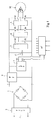
- FIG. 1 The general architecture of a conventional motor control circuit is illustrated in FIG. 1.
- This circuit comprises a rectifier bridge 1 connected to the terminals of the sector via a filtering circuit 2. Between the positive output terminals and negative of the rectifier bridge is connected a high value capacitor C intended to store and smooth the direct voltage to be supplied to a load.
- a control circuit comprising on the one hand adapter circuits 3, 4, 5 coupled to the pairs of switches, on the other hand a microcontroller ⁇ C intended to apply the control signals to the various adapter circuits. It is possible, for example, to use adapter circuits of the L6386 type and a microcontroller of the ST92141 type, both available from the company STMicroelectronics.
- the circuit must include means for power the microcontroller and possibly other elements of the circuit.
- a low power circuit is provided voltage (LPS) 7 providing for example two direct voltages V1 and V2, with respective values 15 V and 5 V.
- the low voltage power circuit 7 is connected between the positive and negative terminals of the same rectifier bridge as that which supplies the main circuit.
- a circuit 9 is generally provided for improving the power factor (PF).
- circuit 9 for improving the power factor is basically to broaden the momentum of current which is extracted from the sector whenever we want recharge the capacitor C, that is to say at each alternation, in order to reduce the current harmonics returned to the mains and therefore reduce the dimensions of the components (inductance and capacity) of filter 2, which also helps to reduce the costs.
- the sum of costs of the low voltage supply circuit and the assembly of the power factor reduction circuit (if any provided a) and the filter is approximately half the cost of the whole circuit.
- the present invention proposes to combine the low voltage supply circuit and the improvement circuit of the power factor.
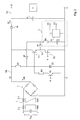
- the present invention provides a circuit for supplying a DC voltage of value high from the rectified output of a rectifier bridge on a high capacity capacitor and supply of voltages low power supply, including a first connected diode between the first output terminal of the rectifier bridge and a first capacitor terminal; first and second transistors mounted in cascode, the first main terminal of the first transistor being connected to the first bridge output terminal rectifier, the second main terminal of the second transistor being connected to the second bridge output terminal; a way to fix the potential of the control terminal of the first transistor at a first voltage with respect to the second terminal of the bridge; means for reducing the potential of said terminal control when the voltage on the first terminal exceeds one predetermined value; a regulation circuit connected to the point connecting the first and second transistors; a second diode connecting the connection point of the first and second transistors at the control terminal of the first transistor; and one means for applying a setting pulse to the second transistor conduction of fixed duration after the output voltage of the bridge has exceeded said determined value.
- the first transistor is an insulated gate bipolar transistor (IGBT).
- IGBT insulated gate bipolar transistor
- the second transistor is a MOS transistor.
- control signals of said means for reducing the potential are provided by a microcontroller from a detection of the output voltage of the rectifier bridge, the output voltage of the first diode, and of the current in this first diode.
- the regulation circuit includes a third connected diode at the connection point of the first and second transistors and a capacitor connected between this diode and the lower terminal of the voltage rectified.
- an embodiment of a circuit according to the present invention uses a rectifier bridge 1.
- the primary of the rectifier bridge is connected to terminals VAC power supply via filter 2 which includes for example, as shown, a capacitor at the terminals of alternating voltage and inductors coupled to the input terminals of the rectifier bridge.
- filter 2 which includes for example, as shown, a capacitor at the terminals of alternating voltage and inductors coupled to the input terminals of the rectifier bridge.
- filter 2 which includes for example, as shown, a capacitor at the terminals of alternating voltage and inductors coupled to the input terminals of the rectifier bridge.
- Inductors 2-2 are of higher values and have the essential role of filtering low frequency components (frequencies below about 1 kHz).
- ferrite core chokes are designed to eliminate high frequency components (frequencies greater than about 1 kHz) which, as will be seen below, does not are not predominant during the operation of the circuit according to the present invention in which the various controls are exercised only at the rhythm of the alternations of the voltage alternative.
- the circuit according to the present invention comprises, between the positive and negative output terminals 10 and 11 of the bridge rectifier 1, the cascode assembly of two transistors T1 and T2.
- the transistor T1 is preferably a voltage-controlled transistor.
- this transistor in front as will be seen below, bear some reverse voltage, we will preferably choose an insulated gate bipolar transistor (IGBT) rather than a transistor Classic MOS.
- Transistor T1 is sized to support the voltage between terminals 10 and 11, i.e. a maximum voltage of the order of 300 volts when the alternating voltage input, VAC, is the line voltage at 220 volts.
- the transistor T2 is a low power transistor, preferably an MOS transistor easily controllable by signals logical.
- the collector of transistor T1 is connected to the terminal 10, the emitter of transistor T1 is connected to the drain of the transistor T2 and the source of transistor T2 is connected to terminal 11.
- the transistor T2 receives on its control terminal a signal Y which will be described below.
- the gate of transistor T1 is polarized by a Zener diode Z1. More particularly, this grid is firstly connected to terminal 10 by a high resistance value R1, on the other hand at terminal 11 by the Zener diode Z1.
- the gate of transistor T1 is capable of being connected to terminal 11 via a switch in series with R2 resistance. In the embodiment shown, this switch consists of a bipolar transistor T3 whose collector is connected to resistor R2 and whose emitter is connected to terminal 11.
- the base of transistor T3 is susceptible receive an X signal.
- the connection point 12 between the transistors T1 and T2 is connected via a diode d1 to a low voltage supply circuit 7.
- the cathode of diode d1 is connected to the terminal 11 via a resistor R3 and a capacitor C1.
- the connection point of resistance R3 and capacitor C1 constitutes a first output terminal to a first low voltage V1.
- This voltage V1 supplies a circuit of conventional regulation 13 providing a second direct voltage regulated V2. It will be noted that the voltage V1 is substantially equal to the Zener voltage of diode Z1 minus the gate-emitter voltage drop of transistor T1 minus the direct voltage drop of diode d1.
- the Zener voltage of diode Z1 will be around 18 volts.
- the voltage V2 will be for example equal to 5 volts.
- the regulation circuit 13 will for example be a circuit available from STMicroelectronics under the reference ST78L05A.
- the circuit comprises between the cathode of the diode d1 and the gate of transistor T1 a recirculation diode d2.
- Terminals 10 and 11 are respectively connected to output terminals 14 and 15, a diode D being inserted between terminals 10 and 14. In the example shown, terminals 11 and 15 are confused. Between terminals 14 and 15 is arranged a high-value capacitor C for storing a voltage continues between recharging phases.
- a charge L could be disposed between terminals 14 and 15 and corresponds for example to a set of six switches S1 to S6 supplying windings motor as described in connection with Figure 1.
- the output current of the rectifier bridge is designated by I B , by V B the output voltage at terminal 10 of the rectifier bridge, by I C the current passing through the diode D and flowing to the capacitor C and / or the load L, and by V A the voltage between the output terminals 14 and 15.
- FIG. 3 represents the dotted lines of the sinusoid arches corresponding to the general shape of the voltage V B and, in solid lines, the current I B taken from the sector by the rectifier bridge 1. It is assumed that one places oneself in a state in which the circuit has already operated, that is to say that the capacitor C is charged at a high voltage slightly lower than the peak value of the voltage V B and that the capacitor C1 is charged at the voltage V1. Thus, at time t 0 , the voltage V B begins to increase and no current flows.
- the conduction of the transistor T1 is interrupted by controlling the conduction of the transistor T3 by a signal X.
- the gate of transistor T1 then discharges.
- the value of the resistor R2 although less than the resistor R1 is sufficiently high for the capacitor C1 to discharge only very slightly during an alternation of the supply voltage.
- the voltage on the gate of the transistor T1 remains substantially equal to the voltage on the capacitor C1, that is to say of the order of 15 volts in the previous example.
- the transistor T2 is open but, during a transient phase, the transistor T1 remains on and the current in the inductors continues to flow between the AC supply terminals. passing from terminal 10 to terminal 11 through transistor T1, diodes d1 and d2 and Zener diode Z1.
- the current decreases progressively in the channel of the transistor T1 according to the closing speed of the transistor T2 then, as soon as the voltage V B on the terminal 10 exceeds the instantaneous value of the voltage V A (instant t 5 ) , the diode D becomes conducting and the flow of current is interrupted in the transistor T1.
- the current supplied by the rectifier bridge is then used to recharge the capacitor C and to supply the load L through the diode D.
- the conduction continues until the voltage V B drops significantly below the value of the voltage V A , which occurs some time after time t 6 .
- the current I B becomes zero until an instant t 7 at which the signal X applied to the base of the transistor T3 re-blocks this transistor so that the voltage on the gate of the transistor T1 goes up and that it recirculates a current in this transistor to recharge capacitor C1.
- a new current passing cycle is thus obtained at the end of the alternation, which has substantially the same appearance as that of the start of the conduction phase. Note, however, that the current peak is normally slightly higher since the time that has elapsed since the previous phase of recharging the capacitor C1 is longer than between time t 7 and time t 1 of the next alternation.
- a circulation of the current I B has been obtained during relatively extended phases of alternating mains voltage. It will be noted that, in the absence of the circuit according to the invention, there would have been a current flow I B substantially only during the phase t 5 -t 6 when the mains voltage becomes greater than the voltage across the capacitor C.
- the signal X can be obtained analogically, for example by connecting the base of transistor T3 to terminal 10 via a resistor and by connecting this base to terminal 11 via a Zener diode having for example a Zener voltage of the order of a hundred volts.
- the control pulse Y can be supplied automatically by detecting the conduction of the transistor T3 then by controlling for a determined period the conduction of the transistor T2 by various known means.
- it will preferably be taken advantage of the fact that the envisaged applications are applications in which a microcontroller is provided, as has been described in relation to FIG.
- this microcontroller will be used to produce the signals X and Y. It will be noted that the conduction time of the transistor T2 makes it possible to regulate the voltage V A and also to ensure an optimization of the shape of the current extracted between the instants t 3 and t 6 and in particular of the value of the minimum of this current, at time t 5 .
- FIG. 4 represents a somewhat embodiment more detailed of the circuit of figure 2 indicating in particular a way to extract the signals needed to control the microprocessor.
- the output voltage of the rectifier bridge appears on terminals 10 and 11 and the voltage across the charge appears between terminals 14 and 15.
- the transistor T3 has been shown as a variant in the form of a MOS transistor, and this does not change the operation of the circuit.
- a capacitor C2 was placed in parallel on the diode Z1 and is intended to avoid voltage oscillations on the gate of transistor T1.
- a divider bridge comprising resistors R5 and R6 is connected between terminals 10 and 11 to supply a voltage v B which constitutes an image of the voltage V B.
- a divider bridge comprising resistors R7 and R8 is connected between terminals 14 and 15 to supply a voltage vA which is an image of the voltage V A.
- a small resistor R9 is arranged in series with the main supply circuit so that the voltage v C at its terminals is an image of the charging current I C , which corresponds to the current flowing in the diode D.
- a low value resistor R10 connected in series with the transistors T1 and T2 so that the voltage v D across its terminals is an image of the current in the main transistor chain.
- This last piece of information can be used as a safety measure to open the transistor T2 if the current becomes too high during the phase t 3 -t 4 .
- the signal X will be at zero as long as the voltage V B is below a determined threshold.
- the duration of the slot Y will be determined so that V A remains lower by a determined value than the peak value of V B and so that the decrease of the current at time t 5 is optimized.
- circuit according to the present invention note that the power dissipated by the supply circuit low supply voltages V1 and V2 is minimum because this circuit only consumes if the power is actually extracted from low voltage sources V1 and V2. In addition, the recharging of these circuits is only provided while the voltage sector is relatively small (less than a value of reference for example equal to 100 volts).
- Another advantage of circuit according to the present invention is that it does not use any moment of components operating at high frequency. Frequency highest command frequency applied is twice the frequency of the sector, i.e. 100 or 120 Hz in the case of the two most common standardized systems.
- Another advantage of the present invention is that the power stage of the voltage regulator and the corrector harmonics is common, which reduces the cost of system.
- the present invention is susceptible of numerous variants and modifications and also applies to circuits of doubler type.
Landscapes
- Engineering & Computer Science (AREA)
- Power Engineering (AREA)
- Rectifiers (AREA)
Applications Claiming Priority (2)
| Application Number | Priority Date | Filing Date | Title |
|---|---|---|---|
| FR9814918 | 1998-11-24 | ||
| FR9814918A FR2786338B1 (fr) | 1998-11-24 | 1998-11-24 | Alimentation continue haute et basse tension |
Publications (1)
| Publication Number | Publication Date |
|---|---|
| EP1005145A1 true EP1005145A1 (de) | 2000-05-31 |
Family
ID=9533232
Family Applications (1)
| Application Number | Title | Priority Date | Filing Date |
|---|---|---|---|
| EP99410166A Withdrawn EP1005145A1 (de) | 1998-11-24 | 1999-11-22 | Hoch- und Niederspannungsgleichstromversorgung |
Country Status (3)
| Country | Link |
|---|---|
| US (1) | US6137701A (de) |
| EP (1) | EP1005145A1 (de) |
| FR (1) | FR2786338B1 (de) |
Cited By (1)
| Publication number | Priority date | Publication date | Assignee | Title |
|---|---|---|---|---|
| CN111082403A (zh) * | 2020-01-09 | 2020-04-28 | 华北电力大学 | 一种适用于二极管桥的一体化叠层母排结构 |
Families Citing this family (5)
| Publication number | Priority date | Publication date | Assignee | Title |
|---|---|---|---|---|
| JP2001284267A (ja) * | 2000-04-03 | 2001-10-12 | Canon Inc | 排気処理方法、プラズマ処理方法及びプラズマ処理装置 |
| AU2002252564A1 (en) * | 2001-03-30 | 2002-10-15 | Youtility Inc | Enhanced conduction angle power factor correction topology |
| ITMI20040356A1 (it) * | 2004-02-27 | 2004-05-27 | St Microelectronics Srl | Circuito di pilotaggio di una configurazione emitter switching per controllare il livello di saturazione di un transistore di potenza in applicazioni che prevedono correnti di collettoree variabili in un ampio intervallo |
| US10177678B2 (en) * | 2014-01-13 | 2019-01-08 | Philips Lighting Holding B.V. | Buffering capacitor for diode bridge rectifier with controlled decharging current |
| CN113904611B (zh) * | 2021-10-15 | 2025-05-13 | 珠海格力节能环保制冷技术研究中心有限公司 | 电压驱动电路、系统及家电设备 |
Citations (2)
| Publication number | Priority date | Publication date | Assignee | Title |
|---|---|---|---|---|
| DE4028348A1 (de) * | 1990-09-06 | 1992-03-12 | Zumtobel Ag | Niederspannungsquelle mit vorschaltanordnung |
| EP0743742A1 (de) * | 1995-05-09 | 1996-11-20 | STMicroelectronics S.A. | Leistungsfaktorverbesserung für eine gleichgerichtete Leistungsversorgung |
Family Cites Families (5)
| Publication number | Priority date | Publication date | Assignee | Title |
|---|---|---|---|---|
| NL8500154A (nl) * | 1985-01-22 | 1986-08-18 | Koninkl Philips Electronics Nv | Zelf-oscillerende voedingsschakeling. |
| US4965506A (en) * | 1989-02-14 | 1990-10-23 | U.S. Philips Corporation | Power-supply circuit having circuitry for switching from a battery charging mode to a battery trickle-charging mode |
| DE4122544C1 (de) * | 1991-07-08 | 1992-07-16 | Braun Ag, 6000 Frankfurt, De | |
| ATE190781T1 (de) * | 1995-11-27 | 2000-04-15 | Koninkl Philips Electronics Nv | Stromversorgungsschaltung |
| DE69602422T2 (de) * | 1995-11-27 | 1999-11-25 | Koninklijke Philips Electronics N.V., Eindhoven | Stromversorgungsschaltung |
-
1998
- 1998-11-24 FR FR9814918A patent/FR2786338B1/fr not_active Expired - Fee Related
-
1999
- 1999-11-22 EP EP99410166A patent/EP1005145A1/de not_active Withdrawn
- 1999-11-22 US US09/444,592 patent/US6137701A/en not_active Expired - Lifetime
Patent Citations (2)
| Publication number | Priority date | Publication date | Assignee | Title |
|---|---|---|---|---|
| DE4028348A1 (de) * | 1990-09-06 | 1992-03-12 | Zumtobel Ag | Niederspannungsquelle mit vorschaltanordnung |
| EP0743742A1 (de) * | 1995-05-09 | 1996-11-20 | STMicroelectronics S.A. | Leistungsfaktorverbesserung für eine gleichgerichtete Leistungsversorgung |
Cited By (2)
| Publication number | Priority date | Publication date | Assignee | Title |
|---|---|---|---|---|
| CN111082403A (zh) * | 2020-01-09 | 2020-04-28 | 华北电力大学 | 一种适用于二极管桥的一体化叠层母排结构 |
| CN111082403B (zh) * | 2020-01-09 | 2021-01-08 | 华北电力大学 | 一种适用于二极管桥的一体化叠层母排结构 |
Also Published As
| Publication number | Publication date |
|---|---|
| US6137701A (en) | 2000-10-24 |
| FR2786338B1 (fr) | 2001-02-09 |
| FR2786338A1 (fr) | 2000-05-26 |
Similar Documents
| Publication | Publication Date | Title |
|---|---|---|
| EP3422554B1 (de) | Reversibler ac/dc-wandler mit thyristoren | |
| EP1626493A1 (de) | Kapazitives Netzteil | |
| EP1914871A1 (de) | Schaltnetzteilsystem und Regelantrieb mit einem solchen System | |
| EP0448434B1 (de) | Gleichrichter für mindestens zwei Versorgungswechselspannungsbereiche | |
| FR2734424A1 (fr) | Dispositif d'alimentation electronique | |
| FR2742013A1 (fr) | Procede et dispositif de limitation d'appel de courant d'un condensateur associe a un redresseur | |
| EP3010133B1 (de) | Anordnung zur kontrollierten gleichrichtung | |
| FR2743953A1 (fr) | Circuit d'alimentation a condensateur de stockage | |
| WO2013056918A1 (fr) | Convertisseur de puissance et son circuit de pre-charge | |
| FR3122793A1 (fr) | Circuit électronique avec thyristor | |
| FR2811490A1 (fr) | Unite de commande de tension pour un generateur de courant alternatif vehiculaire | |
| EP0820141B1 (de) | Nullspannungsansteuerung einer hybriden Brückenschaltung | |
| EP1005145A1 (de) | Hoch- und Niederspannungsgleichstromversorgung | |
| FR2734429A1 (fr) | Module interrupteur et d'alimentation-application au demarrage d'un tube fluorescent | |
| EP0772280A1 (de) | Gleichgerichtete Doppelspannungsversorgungskreis | |
| FR2706226A1 (fr) | Dispositif de commande de variation de puissance et/ou de vitesse d'une charge, tel que d'un moteur ou autre. | |
| EP0798838B1 (de) | Schaltung zur Verbesserung des Leistungsfaktors mit doppelter Entladung | |
| EP1646132A2 (de) | Doppelte Versorgungsschaltung | |
| FR2783370A1 (fr) | Dispositif d'alimentation a onduleur dont la puissance delivree est controlee | |
| FR2859580A1 (fr) | Gradateur pour charges resistives ou capacitives | |
| EP1061650A1 (de) | Bistabiler Zweirichtungs-Hochspannungsschalter | |
| EP0955718A1 (de) | Schaltspannungswandler | |
| EP0821469A1 (de) | Hoch- und Niederspannungsgleichstromversorgung | |
| BE1012238A4 (fr) | Circuit redresseur-lisseur. | |
| EP1434340B1 (de) | Isolierte Niederspannungsversorgung |
Legal Events
| Date | Code | Title | Description |
|---|---|---|---|
| PUAI | Public reference made under article 153(3) epc to a published international application that has entered the european phase |
Free format text: ORIGINAL CODE: 0009012 |
|
| AK | Designated contracting states |
Kind code of ref document: A1 Designated state(s): DE FR GB IT |
|
| AX | Request for extension of the european patent |
Free format text: AL;LT;LV;MK;RO;SI |
|
| 17P | Request for examination filed |
Effective date: 20001122 |
|
| AKX | Designation fees paid |
Free format text: DE FR GB IT |
|
| RAP1 | Party data changed (applicant data changed or rights of an application transferred) |
Owner name: STMICROELECTRONICS S.A. |
|
| RIC1 | Information provided on ipc code assigned before grant |
Ipc: H02M 1/42 20070101AFI20071204BHEP |
|
| GRAP | Despatch of communication of intention to grant a patent |
Free format text: ORIGINAL CODE: EPIDOSNIGR1 |
|
| STAA | Information on the status of an ep patent application or granted ep patent |
Free format text: STATUS: THE APPLICATION IS DEEMED TO BE WITHDRAWN |
|
| 18D | Application deemed to be withdrawn |
Effective date: 20080603 |