US6137701A - High and low voltage D. C. power supply - Google Patents
High and low voltage D. C. power supply Download PDFInfo
- Publication number
- US6137701A US6137701A US09/444,592 US44459299A US6137701A US 6137701 A US6137701 A US 6137701A US 44459299 A US44459299 A US 44459299A US 6137701 A US6137701 A US 6137701A
- Authority
- US
- United States
- Prior art keywords
- transistor
- voltage
- terminal
- circuit
- diode
- Prior art date
- Legal status (The legal status is an assumption and is not a legal conclusion. Google has not performed a legal analysis and makes no representation as to the accuracy of the status listed.)
- Expired - Lifetime
Links
- 239000003990 capacitor Substances 0.000 claims abstract description 26
- 230000033228 biological regulation Effects 0.000 claims abstract description 8
- 238000001514 detection method Methods 0.000 claims description 2
- 230000006872 improvement Effects 0.000 description 6
- 230000008901 benefit Effects 0.000 description 5
- 230000004075 alteration Effects 0.000 description 2
- 230000001276 controlling effect Effects 0.000 description 2
- 230000007423 decrease Effects 0.000 description 2
- 230000004048 modification Effects 0.000 description 2
- 238000012986 modification Methods 0.000 description 2
- 238000004804 winding Methods 0.000 description 2
- 229910000859 α-Fe Inorganic materials 0.000 description 2
- XEEYBQQBJWHFJM-UHFFFAOYSA-N Iron Chemical group [Fe] XEEYBQQBJWHFJM-UHFFFAOYSA-N 0.000 description 1
- 230000008859 change Effects 0.000 description 1
- 230000003247 decreasing effect Effects 0.000 description 1
- 238000001914 filtration Methods 0.000 description 1
- 238000009499 grossing Methods 0.000 description 1
- 230000001939 inductive effect Effects 0.000 description 1
- 238000005457 optimization Methods 0.000 description 1
- 230000010355 oscillation Effects 0.000 description 1
- 230000009467 reduction Effects 0.000 description 1
- 230000001105 regulatory effect Effects 0.000 description 1
- 230000001052 transient effect Effects 0.000 description 1
- 238000005406 washing Methods 0.000 description 1
Images


Classifications
-
- H—ELECTRICITY
- H02—GENERATION; CONVERSION OR DISTRIBUTION OF ELECTRIC POWER
- H02M—APPARATUS FOR CONVERSION BETWEEN AC AND AC, BETWEEN AC AND DC, OR BETWEEN DC AND DC, AND FOR USE WITH MAINS OR SIMILAR POWER SUPPLY SYSTEMS; CONVERSION OF DC OR AC INPUT POWER INTO SURGE OUTPUT POWER; CONTROL OR REGULATION THEREOF
- H02M1/00—Details of apparatus for conversion
- H02M1/42—Circuits or arrangements for compensating for or adjusting power factor in converters or inverters
- H02M1/4208—Arrangements for improving power factor of AC input
-
- Y—GENERAL TAGGING OF NEW TECHNOLOGICAL DEVELOPMENTS; GENERAL TAGGING OF CROSS-SECTIONAL TECHNOLOGIES SPANNING OVER SEVERAL SECTIONS OF THE IPC; TECHNICAL SUBJECTS COVERED BY FORMER USPC CROSS-REFERENCE ART COLLECTIONS [XRACs] AND DIGESTS
- Y02—TECHNOLOGIES OR APPLICATIONS FOR MITIGATION OR ADAPTATION AGAINST CLIMATE CHANGE
- Y02B—CLIMATE CHANGE MITIGATION TECHNOLOGIES RELATED TO BUILDINGS, e.g. HOUSING, HOUSE APPLIANCES OR RELATED END-USER APPLICATIONS
- Y02B70/00—Technologies for an efficient end-user side electric power management and consumption
- Y02B70/10—Technologies improving the efficiency by using switched-mode power supplies [SMPS], i.e. efficient power electronics conversion e.g. power factor correction or reduction of losses in power supplies or efficient standby modes
Definitions
- the present invention relates to a circuit adapted for providing, from a rectifying bridge, on the one hand, a D.C. power supply intended for supplying a load and, on the other hand, one or several low voltage power supplies for supplying secondary circuits such as control circuits.
- the present invention especially aims at the supply of low power motors, that is, of a power smaller than 1 kilowatt, for example, motors which can be found in many industrial or household applications such as washing machines, vacuum cleaners, fans, etc.
- low power motors that is, of a power smaller than 1 kilowatt, for example, motors which can be found in many industrial or household applications such as washing machines, vacuum cleaners, fans, etc.
- two constraints are imposed. The first one is that the circuit must be of low cost, the second one being that the circuit sends back a minimum amount of electric noise onto the mains.
- FIG. 1 The general architecture of a conventional motor control circuit is illustrated in FIG. 1.
- This circuit includes a rectifying bridge 1 connected across the mains via a filtering circuit 2. Between the positive and negative output terminals of the rectifying bridge is connected a capacitor of high value C intended for storing and smoothing the D.C. voltage to be supplied to a load.
- a capacitor of high value C intended for storing and smoothing the D.C. voltage to be supplied to a load.
- three bridge arms each including two switches S1-S2, S3-S4, S5-S6 are, for example, provided.
- a control circuit including, on the one hand, adapter circuits 3, 4, 5 coupled to the pairs of switches, and on the other hand, a microcontroller ⁇ C intended for applying the control signals to the various adapter circuits.
- Adapter circuits of type L6386 and a microcontroller of type ST92141, both sold by STMicroelectronics, may, for example, be used.
- the circuit must include means for supplying power to the microcontroller, and possibly other elements of the circuit.
- a low voltage power supply circuit (LPS) 7 providing for example two D.C. voltages V1 and V2, of respective values 15 V and 5 V, is provided.
- low voltage power supply circuit 7 is connected between the positive and negative terminals of the same rectifying bridge as that which supplies the main circuit.
- PF power factor
- the present invention provides combining a low voltage power supply circuit and the power factor improvement circuit.
- the present invention provides a circuit for providing a D.C. voltage of high value from the rectified output of a rectifying bridge on a capacitor of high capacitance, and for providing low supply voltages, including a first diode connected between the first output terminal of the rectifying bridge and a first terminal of the capacitor; first and second cascode-connected transistors, the first main terminal of the first transistor being connected to the first output terminal of the rectifying bridge, the second main terminal of the second transistor being connected to the second output terminal of the bridge; means for setting the potential of the control terminal of the first transistor to a first voltage with respect to the second terminal of the bridge; means for reducing the potential of the control terminal when the voltage on the first terminal exceeds a predetermined value; a regulation circuit connected at the connection node of the first and second transistors; a second diode connecting the connection node of the first and second transistors to the control terminal of the first transistor; and means for applying, to the second transistor, a turn-on pulse of determined duration after the output voltage of the
- the first transistor is an insulated-gate bipolar transistor (IGBT).
- IGBT insulated-gate bipolar transistor
- the second transistor is a MOS transistor.
- control signals of the means for reducing the potential are provided by a microcontroller based on a detection of the output voltage of the rectifying bridge, of the output voltage of the first diode, and of the current in this first diode.
- the regulation circuit includes a third diode connected to the connection node of the first and second transistors and a capacitor connected between this diode and the low terminal of the rectified voltage.
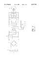
- FIG. 1 previously described, shows the general architecture of a circuit of D.C. supply of a load and of provision of a low voltage
- FIG. 2 schematically shows a simplified embodiment of a circuit according to the present invention
- FIG. 3 shows voltage and current curves intended for illustrating the operation of the circuit according to the present invention.
- FIG. 4 is a more detailed representation of an embodiment of the circuit according to the present invention.
- an embodiment of a circuit according to the present invention uses a rectifying bridge 1.
- the primary of the rectifying bridge is connected to A.C. power supply terminals VAC via a filter 2 which is comprised, for example, of a capacitor across the A.C. voltage and of inductances coupled to the input terminals of the rectifying bridge.
- a pair of inductances with a ferrite core 2-1 and a pair of inductances with an iron core 2-2 have been shown as an example.
- Inductances 2-2 are of high value and function to filter low-frequency components (frequencies under approximately 1 kHz).
- Inductances 2-1 with a ferrite core are intended for suppressing high-frequency components (frequencies greater than approximately 1 kHz) which, as will be seen hereafter, are not excessive during operation of the circuit according to the present invention in which the various control signals are sent only at the rate of the halfwaves of the A.C voltage.
- the circuit according to the present invention includes, between positive and negative output terminals 10 and 11 of rectifying bridge 1, the cascode assembly of two transistors T1 and T2.
- Transistor T1 preferably is a voltage-controlled transistor. Further, since this transistor must, as will be seen hereafter, withstand a given reverse voltage without breaking down, an IGBT transistor will preferably be chosen rather than a conventional MOS transistor.
- Transistor T1 is sized to withstand the voltage between terminals 10 and 11, that is, a maximum voltage on the order of 300 volts when the A.C. input voltage, VAC, is the 220-volt mains voltage.
- Transistor T2 is a low power transistor, preferably a MOS transistor easily controllable by logic signals.
- the collector of transistor T1 is connected to terminal 10, the emitter of transistor T1 is connected to the drain of transistor T2, and the source of transistor T2 is connected to terminal 11.
- Transistor T2 receives, on its control terminal, a signal Y which will be described hereafter.
- the gate of transistor T1 is biased by a zener diode Z1. More specifically, this gate is connected, on the one hand, to terminal 10 by a resistor of high value R1, and, on the other hand, to terminal 11 by zener diode Z1. Further, the gate of transistor T1 is capable of being connected to terminal 11 via a switch in series with a resistor R2.
- this switch is formed of a bipolar transistor T3, the collector of which is connected to resistor R2 and the emitter of which is connected to terminal 11.
- the base of transistor T3 is capable of receiving a signal X.
- Connection node 12 between transistors T1 and T2 is connected via a diode d1 to a low voltage power supply circuit 7.
- the cathode of diode d1 is connected to terminal 11 via a resistor R3 and a capacitor C1.
- the connection node of resistor R3 with capacitor C1 forms a first output terminal at a first low voltage V1.
- Voltage V1 supplies a conventional regulation circuit 13 providing a second D.C. regulated voltage V2.
- voltage V1 is substantially equal to the zener voltage of diode Z 1 minus the gate-emitter voltage of transistor T1, minus the forward voltage drop of diode d1.
- the zener voltage of diode Z1 will be on the order of 18 volts.
- Voltage V2 will for example be equal to 5 volts.
- Regulation circuit 13 can, for example, be a circuit sold by STMicroelectronics under reference ST78L05A.
- the circuit includes between the cathode of diode d1 and the gate of transistor T1 a recirculation diode d2.
- Terminals 10 and 11 are respectively connected to output terminals 14 and 15, a diode D being inserted between terminals 10 and 14. In the example shown, terminals 11 and 15 are confounded. Between terminals 14 and 15 is arranged a capacitor of high value C intended for storing a D.C. voltage between recharge phases.
- a load L may be arranged between terminals 14 and 15 and for example corresponds to an assembly of six switches S1 to S6 supplying motor windings as described in relation with FIG. 1.
- IB designates the output voltage of the rectifying bridge
- VB designates the output voltage on terminal 10 of the rectifying bridge
- IC designates the current flowing through diode D and flowing towards capacitor C and/or load L
- VA designates the voltage between output terminals 14 and 15.
- FIG. 3 shows, in dotted lines, sinusoid arches corresponding to the general shape of voltage VB and, in full line, current IB drawn from the mains by rectifying bridge 1. It is assumed to be in a state where the circuit has already operated, that is, capacitor C is charged to a high voltage slightly lower than the peak value of voltage VB and capacitor C1 is charged to voltage V1. Thus, at time t0, voltage VB starts decreasing and no current flows.
- transistor T1 turns on.
- the gate voltage of this transistor then settles at a value slightly greater than this value of turning on by diode Z1.
- a relatively high current flows through transistor T1, diode d1, and resistor R3 to recharge capacitor C1.
- this current settles at a smaller value corresponding to the power consumption on low voltage supply sources V1 and V2.
- the conduction of transistor T1 is interrupted by controlling with a signal X the turning-on of transistor T3.
- the gate of transistor T1 then discharges.
- the value of resistance R2, although smaller than resistance R1 is sufficiently high to have capacitor C1 only slightly discharge during a halfwave of the supply voltage.
- the gate voltage of transistor T1 remains substantially equal to the voltage on capacitor C1, that is, on the order of 15 volts in the preceding example.
- transistor T1 Immediately after the turning-on of transistor T3, a voltage pulse Y is applied on the gate of transistor T2 to turn it on for a short time.
- the potential on the emitter of transistor T1 abruptly drops while its gate, biased by capacitor C1 through resistor R3 and diode d2, still is at a high level.
- transistor T1 turns back on.
- the current flows through transistors T1 and T2 as well as through inductances 2-1 and 2-2 and very rapidly increases until a time t4 which corresponds to the end of pulse Y applied to the gate of transistor T3.
- the mains voltage between terminals 10 and 11 is totally applied to inductances 2-1, 2-2 which store power.
- transistor T2 is off but, during a transient phase, transistor T1 remains on and the current through the inductances keeps on flowing between the A.C. supply terminals by flowing from terminal 10 to terminal 11 through transistor T1, diodes d1 and d2, and zener diode Z1.
- the current progressively decreases in the channel of transistor T1 according to the closing rate of transistor T2 and then, as soon as voltage VB on terminal 10 exceeds the instantaneous value of voltage VA (time t5), diode D turns on and the current flow stops in transistor T1.
- the current provided by the rectifying bridge is then used to recharge capacitor C and to supply load L through diode D.
- the conduction continues until voltage VB clearly falls under the value of voltage VA, which occurs some time after time t6.
- Signal X can be obtained in an analog way, for example, by connecting the base of transistor T3 to terminal 10 via a resistor and by connecting this base to terminal 11 via a zener diode having, for example, a zener voltage on the order of some hundred volts.
- Control pulse Y can be automatically provided by detecting the turning-on of transistor T3, and then by controlling for a determined duration the conduction of transistor T2 by various known means.
- advantage will preferably taken from the fact that the envisaged applications are applications in which a microcontroller is provided, as described in relation with FIG.
- this microcontroller will be used to generate signals X and Y. It should be noted that the duration of conduction of transistor T2 enables ensuring a regulation of voltage VA and also ensuring an optimization of the shape of the current extracted between times t3 and t6, and especially of the minimum value of this current, at time t5.
- FIG. 4 shows a rather more detailed embodiment of the circuit of FIG. 2 especially indicating a way of extracting the signals required to control the microprocessor.
- the output voltage of the rectifying bridge appears on terminals 10 and 11 and the voltage across the load appears between terminals 14 and 15.
- Transistor T3 has been shown as an alternative in the form of a MOS transistor, and this does not change the circuit operation.
- a capacitor C2 has been arranged in parallel on diode Z1 and is reduces or prevents voltage oscillations on the gate of transistor T1.
- a dividing bridge including resistors R5 and R6 is connected between terminals 10 and 11 to provide a voltage vB which forms an image of voltage VB.
- a dividing bridge including resistors R7 and R8 is connected between terminals 14 and 15 to provide a voltage vA which is an image of voltage VA.
- a small resistor R9 is connected in series with the main supply circuit so that voltage vC thereacross is an image of charge current IC, which corresponds to the current flowing through diode D.
- a resistor of low value RI0 connected in series with transistors T1 and T2 so that voltage vD thereacross is an image of the current in the main transistor chain may be provided.
- This last information may be used as a security to turn off transistor T2 if the current becomes too high during phase t3-t4.
- Signal X will be at zero as long as voltage VB will be under a determined threshold.
- the duration of rectangular pulse Y will be determined so that VA remains smaller by a determined value than the peak value of VB and so that the current decrease at time t5 is optimized.
- the power dissipated by the circuit for supplying low supply voltages V1 and V2 is minimum since this circuit only consumes power if the power is effectively extracted from low voltage sources V1 and V2. Further, the recharge of these circuits is provided only while the mains voltage is relatively low (under a reference value, for example, equal to 100 volts).
- Another advantage of the circuit according to the present invention is that it uses at no time components operating at high frequency. The highest control frequency among the frequencies applied is double the mains frequency, that is, 100 or 120 Hz in the case of the two most current standardized systems.
- Another advantage of the present invention is that the power stage of the voltage regulator and of the harmonics corrector is common to both, which reduces the system cost.
Landscapes
- Engineering & Computer Science (AREA)
- Power Engineering (AREA)
- Rectifiers (AREA)
Applications Claiming Priority (2)
| Application Number | Priority Date | Filing Date | Title |
|---|---|---|---|
| FR9814918 | 1998-11-24 | ||
| FR9814918A FR2786338B1 (fr) | 1998-11-24 | 1998-11-24 | Alimentation continue haute et basse tension |
Publications (1)
| Publication Number | Publication Date |
|---|---|
| US6137701A true US6137701A (en) | 2000-10-24 |
Family
ID=9533232
Family Applications (1)
| Application Number | Title | Priority Date | Filing Date |
|---|---|---|---|
| US09/444,592 Expired - Lifetime US6137701A (en) | 1998-11-24 | 1999-11-22 | High and low voltage D. C. power supply |
Country Status (3)
| Country | Link |
|---|---|
| US (1) | US6137701A (de) |
| EP (1) | EP1005145A1 (de) |
| FR (1) | FR2786338B1 (de) |
Cited By (5)
| Publication number | Priority date | Publication date | Assignee | Title |
|---|---|---|---|---|
| WO2002080347A3 (en) * | 2001-03-30 | 2002-11-28 | Youtility Inc | Enhanced conduction angle power factor correction topology |
| US20050194623A1 (en) * | 2004-02-27 | 2005-09-08 | Stmicroelectronics S.R.I. | Driven circuit of an emitter switching configuration to control the saturation level of a power transistor when used with highly variable collector currents |
| US20070169890A1 (en) * | 2000-04-03 | 2007-07-26 | Canon Kabushiki Kaisha | Exhaust processing method, plasma processing method and plasma processing apparatus |
| US20160329826A1 (en) * | 2014-01-13 | 2016-11-10 | Philips Lighting Holding B.V. | Buffering capacitor for diode bridge rectifier with controlled decharging current |
| CN113904611A (zh) * | 2021-10-15 | 2022-01-07 | 珠海格力节能环保制冷技术研究中心有限公司 | 电压驱动电路、系统及家电设备 |
Families Citing this family (1)
| Publication number | Priority date | Publication date | Assignee | Title |
|---|---|---|---|---|
| CN111082403B (zh) * | 2020-01-09 | 2021-01-08 | 华北电力大学 | 一种适用于二极管桥的一体化叠层母排结构 |
Citations (7)
| Publication number | Priority date | Publication date | Assignee | Title |
|---|---|---|---|---|
| US4652984A (en) * | 1985-01-22 | 1987-03-24 | U.S. Philips Corporation | Self-oscillating power-supply circuit |
| US4965506A (en) * | 1989-02-14 | 1990-10-23 | U.S. Philips Corporation | Power-supply circuit having circuitry for switching from a battery charging mode to a battery trickle-charging mode |
| DE4028348A1 (de) * | 1990-09-06 | 1992-03-12 | Zumtobel Ag | Niederspannungsquelle mit vorschaltanordnung |
| US5479330A (en) * | 1991-07-08 | 1995-12-26 | Braun Aktiengesellschaft | Electronic switch network part for supplying current to an accumulator with a blocking oscillator type converter |
| US5798914A (en) * | 1995-05-09 | 1998-08-25 | Sgs-Thomson Microelectronics S.A. | Power factor of a rectified power supply |
| US5847940A (en) * | 1995-11-27 | 1998-12-08 | U.S. Philips Corporation | Power-supply circuit |
| US5852549A (en) * | 1995-11-27 | 1998-12-22 | U.S. Philips Corporation | Power-supply circuit |
-
1998
- 1998-11-24 FR FR9814918A patent/FR2786338B1/fr not_active Expired - Fee Related
-
1999
- 1999-11-22 EP EP99410166A patent/EP1005145A1/de not_active Withdrawn
- 1999-11-22 US US09/444,592 patent/US6137701A/en not_active Expired - Lifetime
Patent Citations (7)
| Publication number | Priority date | Publication date | Assignee | Title |
|---|---|---|---|---|
| US4652984A (en) * | 1985-01-22 | 1987-03-24 | U.S. Philips Corporation | Self-oscillating power-supply circuit |
| US4965506A (en) * | 1989-02-14 | 1990-10-23 | U.S. Philips Corporation | Power-supply circuit having circuitry for switching from a battery charging mode to a battery trickle-charging mode |
| DE4028348A1 (de) * | 1990-09-06 | 1992-03-12 | Zumtobel Ag | Niederspannungsquelle mit vorschaltanordnung |
| US5479330A (en) * | 1991-07-08 | 1995-12-26 | Braun Aktiengesellschaft | Electronic switch network part for supplying current to an accumulator with a blocking oscillator type converter |
| US5798914A (en) * | 1995-05-09 | 1998-08-25 | Sgs-Thomson Microelectronics S.A. | Power factor of a rectified power supply |
| US5847940A (en) * | 1995-11-27 | 1998-12-08 | U.S. Philips Corporation | Power-supply circuit |
| US5852549A (en) * | 1995-11-27 | 1998-12-22 | U.S. Philips Corporation | Power-supply circuit |
Non-Patent Citations (1)
| Title |
|---|
| French Search Report from French Patent Application 98 14918, filed Nov. 24, 1998. * |
Cited By (9)
| Publication number | Priority date | Publication date | Assignee | Title |
|---|---|---|---|---|
| US20070169890A1 (en) * | 2000-04-03 | 2007-07-26 | Canon Kabushiki Kaisha | Exhaust processing method, plasma processing method and plasma processing apparatus |
| WO2002080347A3 (en) * | 2001-03-30 | 2002-11-28 | Youtility Inc | Enhanced conduction angle power factor correction topology |
| US6567283B2 (en) * | 2001-03-30 | 2003-05-20 | Youtility Inc. | Enhanced conduction angle power factor correction topology |
| US20050194623A1 (en) * | 2004-02-27 | 2005-09-08 | Stmicroelectronics S.R.I. | Driven circuit of an emitter switching configuration to control the saturation level of a power transistor when used with highly variable collector currents |
| US7449935B2 (en) * | 2004-02-27 | 2008-11-11 | Stmicroelectronics S.R.L. | Driven circuit of an emitter switching configuration to control the saturation level of a power transistor when used with highly variable collector currents |
| US20160329826A1 (en) * | 2014-01-13 | 2016-11-10 | Philips Lighting Holding B.V. | Buffering capacitor for diode bridge rectifier with controlled decharging current |
| US10177678B2 (en) * | 2014-01-13 | 2019-01-08 | Philips Lighting Holding B.V. | Buffering capacitor for diode bridge rectifier with controlled decharging current |
| CN113904611A (zh) * | 2021-10-15 | 2022-01-07 | 珠海格力节能环保制冷技术研究中心有限公司 | 电压驱动电路、系统及家电设备 |
| US12334838B2 (en) | 2021-10-15 | 2025-06-17 | Gree Green Refrigeration Technology Center Co., Ltd. Of Zhuhai | Voltage driving circuit and system and household appliance |
Also Published As
| Publication number | Publication date |
|---|---|
| FR2786338B1 (fr) | 2001-02-09 |
| EP1005145A1 (de) | 2000-05-31 |
| FR2786338A1 (fr) | 2000-05-26 |
Similar Documents
| Publication | Publication Date | Title |
|---|---|---|
| US6169391B1 (en) | Device for converting high voltage alternating current to low voltage direct current | |
| JPH05207734A (ja) | 切換モード電力源を具える回路装置 | |
| JP5832177B2 (ja) | 力率改善回路 | |
| US5570277A (en) | Switching power supply apparatus | |
| JPH10184973A (ja) | 電磁弁駆動装置 | |
| US20200395866A1 (en) | Thyristor control | |
| US5804951A (en) | Power factor correction circuit | |
| US5995395A (en) | Control of a composite bridge at zero voltage | |
| CN1055183C (zh) | 具有降低的总线谐波负载的开关型电源 | |
| US6137701A (en) | High and low voltage D. C. power supply | |
| US6914394B2 (en) | Supply circuit, in particular for a discharge lamp | |
| US5828562A (en) | Double discharge circuit for improving the power factor | |
| JPH1178U (ja) | 幹線電源で負荷を付勢する回路配置 | |
| EP0746892A1 (de) | Vorreglerstromversorgung mit schutz gegen spannungsschwingungen während des abschaltens | |
| JP3418822B2 (ja) | 突入電流抑制回路 | |
| JP7650736B2 (ja) | バッテリ充電装置、保護装置、及び保護方法 | |
| JPH0783585B2 (ja) | 給電回路 | |
| JP2001069750A (ja) | チョッパ型スイッチング電源 | |
| JP2003189464A (ja) | 突入電流防止回路 | |
| CN110071679B (zh) | 电机控制电路 | |
| JP3509567B2 (ja) | 電源装置 | |
| JP3377744B2 (ja) | スイッチング電源装置 | |
| JP3733675B2 (ja) | インバータ装置、放電灯点灯装置及び照明装置 | |
| JPH1169842A (ja) | 駆動回路 | |
| US6894575B2 (en) | High-voltage oscillator having a fast response time |
Legal Events
| Date | Code | Title | Description |
|---|---|---|---|
| AS | Assignment |
Owner name: SGS-THOMSON MICROELECTRONICS, S.A., FRANCE Free format text: ASSIGNMENT OF ASSIGNORS INTEREST;ASSIGNORS:TESSIER, MAXIME;BOURGEOIS, JEAN-MARIE;RAVON, JEAN-MICHEL;AND OTHERS;REEL/FRAME:010555/0437;SIGNING DATES FROM 20000103 TO 20000121 |
|
| STCF | Information on status: patent grant |
Free format text: PATENTED CASE |
|
| FPAY | Fee payment |
Year of fee payment: 4 |
|
| FEPP | Fee payment procedure |
Free format text: PAYOR NUMBER ASSIGNED (ORIGINAL EVENT CODE: ASPN); ENTITY STATUS OF PATENT OWNER: LARGE ENTITY |
|
| FPAY | Fee payment |
Year of fee payment: 8 |
|
| FPAY | Fee payment |
Year of fee payment: 12 |