EP1005992A2 - Substrat für einen Flüssigkeitsausstosskopf, Flüssigkeitsausstosskopf und Flüssigkeitsausstossgerät - Google Patents
Substrat für einen Flüssigkeitsausstosskopf, Flüssigkeitsausstosskopf und Flüssigkeitsausstossgerät Download PDFInfo
- Publication number
- EP1005992A2 EP1005992A2 EP99309713A EP99309713A EP1005992A2 EP 1005992 A2 EP1005992 A2 EP 1005992A2 EP 99309713 A EP99309713 A EP 99309713A EP 99309713 A EP99309713 A EP 99309713A EP 1005992 A2 EP1005992 A2 EP 1005992A2
- Authority
- EP
- European Patent Office
- Prior art keywords
- liquid
- liquid discharge
- substrate
- discharge head
- movable
- Prior art date
- Legal status (The legal status is an assumption and is not a legal conclusion. Google has not performed a legal analysis and makes no representation as to the accuracy of the status listed.)
- Granted
Links
- 239000007788 liquid Substances 0.000 title claims abstract description 189
- 239000000758 substrate Substances 0.000 title claims abstract description 99
- 239000010410 layer Substances 0.000 claims abstract description 50
- 238000007599 discharging Methods 0.000 claims abstract description 19
- 239000011229 interlayer Substances 0.000 claims abstract description 14
- 238000009413 insulation Methods 0.000 claims abstract description 13
- 238000011144 upstream manufacturing Methods 0.000 claims abstract description 10
- 238000005516 engineering process Methods 0.000 claims description 9
- 229910052581 Si3N4 Inorganic materials 0.000 claims description 6
- 238000000151 deposition Methods 0.000 claims description 5
- HQVNEWCFYHHQES-UHFFFAOYSA-N silicon nitride Chemical compound N12[Si]34N5[Si]62N3[Si]51N64 HQVNEWCFYHHQES-UHFFFAOYSA-N 0.000 claims description 5
- 238000012876 topography Methods 0.000 claims 1
- 239000010408 film Substances 0.000 description 94
- 238000000034 method Methods 0.000 description 26
- 238000005530 etching Methods 0.000 description 24
- 230000001681 protective effect Effects 0.000 description 19
- 239000000463 material Substances 0.000 description 17
- 239000005360 phosphosilicate glass Substances 0.000 description 12
- XUIMIQQOPSSXEZ-UHFFFAOYSA-N Silicon Chemical compound [Si] XUIMIQQOPSSXEZ-UHFFFAOYSA-N 0.000 description 11
- 229910052710 silicon Inorganic materials 0.000 description 11
- 239000010703 silicon Substances 0.000 description 11
- 238000004519 manufacturing process Methods 0.000 description 10
- 238000006073 displacement reaction Methods 0.000 description 7
- 230000008569 process Effects 0.000 description 7
- KRHYYFGTRYWZRS-UHFFFAOYSA-N Fluorane Chemical compound F KRHYYFGTRYWZRS-UHFFFAOYSA-N 0.000 description 6
- 230000015572 biosynthetic process Effects 0.000 description 6
- 230000008859 change Effects 0.000 description 5
- 239000002184 metal Substances 0.000 description 5
- 229910052751 metal Inorganic materials 0.000 description 5
- 238000000059 patterning Methods 0.000 description 5
- 239000004033 plastic Substances 0.000 description 5
- 229920003023 plastic Polymers 0.000 description 5
- VYPSYNLAJGMNEJ-UHFFFAOYSA-N Silicium dioxide Chemical compound O=[Si]=O VYPSYNLAJGMNEJ-UHFFFAOYSA-N 0.000 description 4
- 238000004458 analytical method Methods 0.000 description 4
- 238000001312 dry etching Methods 0.000 description 4
- 230000000694 effects Effects 0.000 description 4
- 239000004744 fabric Substances 0.000 description 4
- 239000000203 mixture Substances 0.000 description 4
- 239000004065 semiconductor Substances 0.000 description 4
- 229910052814 silicon oxide Inorganic materials 0.000 description 4
- 239000000919 ceramic Substances 0.000 description 3
- 230000006378 damage Effects 0.000 description 3
- 239000007789 gas Substances 0.000 description 3
- 239000012535 impurity Substances 0.000 description 3
- 238000011835 investigation Methods 0.000 description 3
- 239000010985 leather Substances 0.000 description 3
- 238000001020 plasma etching Methods 0.000 description 3
- 238000001454 recorded image Methods 0.000 description 3
- 238000004528 spin coating Methods 0.000 description 3
- 238000001039 wet etching Methods 0.000 description 3
- 239000002023 wood Substances 0.000 description 3
- QGZKDVFQNNGYKY-UHFFFAOYSA-N Ammonia Chemical compound N QGZKDVFQNNGYKY-UHFFFAOYSA-N 0.000 description 2
- MCMNRKCIXSYSNV-UHFFFAOYSA-N Zirconium dioxide Chemical compound O=[Zr]=O MCMNRKCIXSYSNV-UHFFFAOYSA-N 0.000 description 2
- 230000009471 action Effects 0.000 description 2
- 239000000853 adhesive Substances 0.000 description 2
- 230000001070 adhesive effect Effects 0.000 description 2
- 239000003513 alkali Substances 0.000 description 2
- QVGXLLKOCUKJST-UHFFFAOYSA-N atomic oxygen Chemical compound [O] QVGXLLKOCUKJST-UHFFFAOYSA-N 0.000 description 2
- 238000009835 boiling Methods 0.000 description 2
- 238000010586 diagram Methods 0.000 description 2
- 238000004043 dyeing Methods 0.000 description 2
- 229910052760 oxygen Inorganic materials 0.000 description 2
- 239000001301 oxygen Substances 0.000 description 2
- 230000000704 physical effect Effects 0.000 description 2
- 238000005268 plasma chemical vapour deposition Methods 0.000 description 2
- 239000002210 silicon-based material Substances 0.000 description 2
- 238000004544 sputter deposition Methods 0.000 description 2
- 239000000126 substance Substances 0.000 description 2
- 235000017166 Bambusa arundinacea Nutrition 0.000 description 1
- 235000017491 Bambusa tulda Nutrition 0.000 description 1
- OKTJSMMVPCPJKN-UHFFFAOYSA-N Carbon Chemical compound [C] OKTJSMMVPCPJKN-UHFFFAOYSA-N 0.000 description 1
- RYGMFSIKBFXOCR-UHFFFAOYSA-N Copper Chemical compound [Cu] RYGMFSIKBFXOCR-UHFFFAOYSA-N 0.000 description 1
- 244000126211 Hericium coralloides Species 0.000 description 1
- 244000082204 Phyllostachys viridis Species 0.000 description 1
- 235000015334 Phyllostachys viridis Nutrition 0.000 description 1
- BLRPTPMANUNPDV-UHFFFAOYSA-N Silane Chemical compound [SiH4] BLRPTPMANUNPDV-UHFFFAOYSA-N 0.000 description 1
- 229910004200 TaSiN Inorganic materials 0.000 description 1
- 238000002679 ablation Methods 0.000 description 1
- 238000009825 accumulation Methods 0.000 description 1
- 239000002253 acid Substances 0.000 description 1
- 238000007792 addition Methods 0.000 description 1
- 229910052782 aluminium Inorganic materials 0.000 description 1
- XAGFODPZIPBFFR-UHFFFAOYSA-N aluminium Chemical compound [Al] XAGFODPZIPBFFR-UHFFFAOYSA-N 0.000 description 1
- PNEYBMLMFCGWSK-UHFFFAOYSA-N aluminium oxide Inorganic materials [O-2].[O-2].[O-2].[Al+3].[Al+3] PNEYBMLMFCGWSK-UHFFFAOYSA-N 0.000 description 1
- 229910021529 ammonia Inorganic materials 0.000 description 1
- 229910003481 amorphous carbon Inorganic materials 0.000 description 1
- 230000003466 anti-cipated effect Effects 0.000 description 1
- 238000004380 ashing Methods 0.000 description 1
- 239000011425 bamboo Substances 0.000 description 1
- 239000002585 base Substances 0.000 description 1
- 230000005540 biological transmission Effects 0.000 description 1
- 229910052799 carbon Inorganic materials 0.000 description 1
- 238000003763 carbonization Methods 0.000 description 1
- 230000015556 catabolic process Effects 0.000 description 1
- 238000006243 chemical reaction Methods 0.000 description 1
- 239000011248 coating agent Substances 0.000 description 1
- 238000000576 coating method Methods 0.000 description 1
- 238000004891 communication Methods 0.000 description 1
- 238000007796 conventional method Methods 0.000 description 1
- 229910052802 copper Inorganic materials 0.000 description 1
- 239000010949 copper Substances 0.000 description 1
- 238000005034 decoration Methods 0.000 description 1
- 230000008021 deposition Effects 0.000 description 1
- 230000006866 deterioration Effects 0.000 description 1
- 238000011161 development Methods 0.000 description 1
- 229910003460 diamond Inorganic materials 0.000 description 1
- 239000010432 diamond Substances 0.000 description 1
- 238000010494 dissociation reaction Methods 0.000 description 1
- 230000005593 dissociations Effects 0.000 description 1
- 239000000428 dust Substances 0.000 description 1
- 238000010292 electrical insulation Methods 0.000 description 1
- 230000002708 enhancing effect Effects 0.000 description 1
- 239000000835 fiber Substances 0.000 description 1
- 239000011521 glass Substances 0.000 description 1
- 230000020169 heat generation Effects 0.000 description 1
- 230000006872 improvement Effects 0.000 description 1
- 230000006698 induction Effects 0.000 description 1
- 239000002649 leather substitute Substances 0.000 description 1
- 238000004518 low pressure chemical vapour deposition Methods 0.000 description 1
- 230000007246 mechanism Effects 0.000 description 1
- 238000005457 optimization Methods 0.000 description 1
- 238000000206 photolithography Methods 0.000 description 1
- 239000011120 plywood Substances 0.000 description 1
- 238000012545 processing Methods 0.000 description 1
- 230000002035 prolonged effect Effects 0.000 description 1
- 230000001902 propagating effect Effects 0.000 description 1
- 230000002040 relaxant effect Effects 0.000 description 1
- 230000004044 response Effects 0.000 description 1
- 230000000717 retained effect Effects 0.000 description 1
- 238000007790 scraping Methods 0.000 description 1
- 229910000077 silane Inorganic materials 0.000 description 1
- 230000007480 spreading Effects 0.000 description 1
- 238000003892 spreading Methods 0.000 description 1
- 230000000087 stabilizing effect Effects 0.000 description 1
- 239000010409 thin film Substances 0.000 description 1
Images


Classifications
-
- B—PERFORMING OPERATIONS; TRANSPORTING
- B41—PRINTING; LINING MACHINES; TYPEWRITERS; STAMPS
- B41J—TYPEWRITERS; SELECTIVE PRINTING MECHANISMS, i.e. MECHANISMS PRINTING OTHERWISE THAN FROM A FORME; CORRECTION OF TYPOGRAPHICAL ERRORS
- B41J2/00—Typewriters or selective printing mechanisms characterised by the printing or marking process for which they are designed
- B41J2/005—Typewriters or selective printing mechanisms characterised by the printing or marking process for which they are designed characterised by bringing liquid or particles selectively into contact with a printing material
- B41J2/01—Ink jet
- B41J2/135—Nozzles
- B41J2/14—Structure thereof only for on-demand ink jet heads
- B41J2/14016—Structure of bubble jet print heads
- B41J2/14032—Structure of the pressure chamber
- B41J2/14048—Movable member in the chamber
-
- B—PERFORMING OPERATIONS; TRANSPORTING
- B41—PRINTING; LINING MACHINES; TYPEWRITERS; STAMPS
- B41J—TYPEWRITERS; SELECTIVE PRINTING MECHANISMS, i.e. MECHANISMS PRINTING OTHERWISE THAN FROM A FORME; CORRECTION OF TYPOGRAPHICAL ERRORS
- B41J2/00—Typewriters or selective printing mechanisms characterised by the printing or marking process for which they are designed
- B41J2/005—Typewriters or selective printing mechanisms characterised by the printing or marking process for which they are designed characterised by bringing liquid or particles selectively into contact with a printing material
- B41J2/01—Ink jet
- B41J2/135—Nozzles
- B41J2/14—Structure thereof only for on-demand ink jet heads
- B41J2/14016—Structure of bubble jet print heads
- B41J2/14032—Structure of the pressure chamber
- B41J2/14056—Plural heating elements per ink chamber
-
- B—PERFORMING OPERATIONS; TRANSPORTING
- B41—PRINTING; LINING MACHINES; TYPEWRITERS; STAMPS
- B41J—TYPEWRITERS; SELECTIVE PRINTING MECHANISMS, i.e. MECHANISMS PRINTING OTHERWISE THAN FROM A FORME; CORRECTION OF TYPOGRAPHICAL ERRORS
- B41J2/00—Typewriters or selective printing mechanisms characterised by the printing or marking process for which they are designed
- B41J2/005—Typewriters or selective printing mechanisms characterised by the printing or marking process for which they are designed characterised by bringing liquid or particles selectively into contact with a printing material
- B41J2/01—Ink jet
- B41J2/135—Nozzles
- B41J2/14—Structure thereof only for on-demand ink jet heads
- B41J2/14016—Structure of bubble jet print heads
- B41J2/14072—Electrical connections, e.g. details on electrodes, connecting the chip to the outside...
Definitions
- the present invention relates to a liquid discharge head and a liquid discharge apparatus for discharging desired liquid by generation of a bubble induced by action of thermal energy on the liquid, and more particularly to the configuration of a substrate on which formed is a thermal energy generating element for generating thermal energy.
- the present invention is applicable to an apparatus such as a printer for recording on various recording media such as paper, yarn, fiber, cloth, metal, plastics, glass, timber or ceramics, a copying apparatus, a facsimile apparatus provided with a communication system, or a word processor equipped with a printer unit, or to industrial recording apparatus combined with various processing apparatus.
- the "recording" means not only providing the recording medium with a meaningful image such as a character or a graphics but also with a meaningless image such as a pattern.
- bubble jet recording method namely an ink jet recording method of providing ink with an energy such as heat to cause a state change involving an abrupt volumic change in the ink, discharging ink from the discharge opening by an action force based on such state change and depositing the ink onto a recording medium to form an image.
- the recording apparatus employing such bubble jet recording method is generally provided, as disclosed in the U.S. Patent No. 4,723,129, with a discharge opening for discharging ink, an ink path communicating with the discharge opening and an electrothermal converting member provided in the ink path and serving as energy generating means for generating energy for discharging the ink.
- Such recording method has various advantages for example of recording an image of high quality at a high speed with a low noise level, and recording an image of a high resolution or even a color image with a compact apparatus since, in the head executing such recording method, the ink discharge openings can be arranged with a high density. For this reason, the bubble jet recording method is recently employed in various office equipment such as printers, copying machines, facsimile apparatus etc., and even in industrial systems such as fabric dyeing apparatus.
- a driving method for liquid discharge capable of realizing a faster ink discharging speed and satisfactory ink discharge based on stable bubble generation, and, for achieving high-speed recording, there is proposed an improved shape of the liquid path for realizing the liquid discharge head with a faster refilling speed of the liquid into the liquid path.
- the present invention is to improve the fundamental discharge characteristics of the basically conventional method of discharging liquid by forming a bubble, particularly a bubble based on film boiling, in the liquid path, to a level that cannot be anticipated before.
- the present inventors have made intensive investigations in order to provide a novel liquid droplet discharging method utilizing the conventionally unavailable bubble and a head utilizing such method.
- these investigations there have been executed first technical analysis on the function of the movable member in the liquid path, analyzing the principle of the mechanism of the movable member in the liquid path, a second technical analysis on the principle of liquid droplet discharge by the bubble, and third technical analysis on the bubble forming area of the heat generating member for bubble formation, and, through these analyses, there has been established a completely novel technology of positively controlling the bubble by positioning the fulcrum and the free end of the movable member in such a manner that the free end is provided at the side of the discharge opening or at the downstream side and by positioning the movable member so as to be opposed to the heat generating member or the bubble generating area.
- the refilling speed can be significantly improved by giving consideration to the arrangement of the movable member and the structure of the liquid supply path.
- An aspect of the present invention provides a substrate adapted for use in the liquid discharge head for discharging liquid by providing thermal energy thereto and provided with a heat generating member for providing the liquid with thermal energy and a movable member, formed by a photolithographic process and so positioned as to be opposed to the heat generating member and having a fixed end at the upstream end in the liquid flowing direction and a free end at the downstream end, wherein:
- a substrate for use in the liquid discharge head for discharging liquid by giving thermal energy thereto the substrate being surfacially provided with plural heat generating members for providing the thermal energy to the liquid and plural movable members so formed by photolithographic technology as to be opposed to the heat generating members and to be fixed at the upstream side in the flowing direction of the liquid and to have free movable ends at the downstream end, wherein:
- the substrate for the liquid discharge head is provided thereon with a heat generating member for providing the ink with thermal energy, and wirings for applying a voltage to the heat generating member, and has step differences on the surface.
- a movable member is formed so as to be opposed to the heat generating member, and such movable member displaces by the pressure change of the bubble generated in the liquid by the heat generated by the heat generating member, thereby satisfactorily controlling the discharge pressure toward the downstream side of the liquid flowing direction.
- this movable member is formed by a photolithographic process, the movable member bears a step difference if the surface of the substrate has a step difference in an area corresponding to the movable member.
- the movable member is displaced by the pressure change of the bubble as explained above, and the stress is concentrated on the step difference at such displacement. Such stress appears strongly particularly on the fulcrum of the movable member, thus affecting the durability thereof.
- the present invention defines the position or height of the step difference formed on the surface of the substrate for the liquid discharge head, thereby relaxing the force applied to the movable member at the displacement thereof.
- the through hole is provided in a position different from the boundary between the fixing portion and the movable portion of the movable member, whereby the step difference is not present in the vicinity of the fulcrum of the movable member.
- the stress concentration can be relaxed in a portion receiving the largest stress at the displacement of the movable member and the durability thereof can be improved.
- the through hole is positively positioned in the fixing portion of the movable member to improve the adhesion force of the fixing portion and also to improve the reliability of the movable member.
- Such configuration is further preferred because the fixing portions of the plural movable members can be formed in common (in a continuous form) to disperse the stress applied to the foxing portions covering the through hole.
- the shape and film quality of the movable member vary according to the step difference mentioned above. If the step difference is positioned at the boundary between the fixing portion and the movable portion of the movable member, the desired performance may not be achievable not only because of the aforementioned stress concentration but also because of the deterioration in the film quality of the movable member and instability of shape thereof, but the configuration of the present invention enables to stability the shape and film quality of the movable member, thereby allowing to provide the substrate for the liquid discharge head and the liquid discharge head, with high reliability.
- the liquid discharge head of the present invention provided with an element substrate surfacially bearing a heat generating member for providing the liquid with thermal energy, a ceiling plate member bearing a discharge opening for discharging ink and a groove communicating with the discharge opening and constituting a liquid path containing the heat generating member upon being adhered to the element substrate, and a movable member formed by a photolithographic technology so as to be opposed to the heat generating member in the liquid path and to have an end at the upstream side, in the liquid flowing direction, fixed to the element substrate and a free end at the end of the downstream side, is featured by a fact that the above-described substrate of the present invention for the liquid discharge head is employed as the element substrate mentioned above.
- the liquid discharge apparatus of the present invention comprises the above-mentioned liquid discharge head of the present invention, and drive signal supply means for supplying a drive signal for causing the liquid discharge head to discharge liquid.
- the liquid discharge apparatus of the present invention may also comprise the above-mentioned liquid discharge head of the present invention, and recording medium conveying means for conveying a recording medium for receiving the liquid discharged from the liquid discharge head. Further, the liquid discharge apparatus of the present invention is preferably so constructed as to execute recording by depositing the ink onto the recording medium.
- Fig. 1 is a cross-sectional view, in a direction along the liquid path, showing the basic configuration of the liquid discharge head constituting an embodiment of the present invention.
- the liquid discharge head of the present embodiment is provided with an element substrate 1 on which plural heat generating members 2 (only one being illustrated) are formed in parallel manner as the discharge energy generating elements for generating thermal energy for generating a bubble in the liquid, a ceiling plate 3 adhered onto the element substrate 1, and an orifice plate 4 adhered to the front end face of the element substrate 1 and the ceiling plate 3.
- the element substrate 1 is formed by forming a silicon oxide film or a silicon nitride film for electrical insulation and heat accumulation on a substrate such as of silicon and patterning thereon an electrical resistance layer constituting the heat generating member 2 and wirings therefor.
- the wirings serve to apply a voltage to the electrical resistance layer to induce a current therein, thereby generating heat in the heat generating member 2.
- On the wirings and the electrical resistance layer there is formed a protective film for protection from the ink, and an anticavitation film is formed thereon for protection from the cavitation resulting from the vanishing of the ink bubble.
- the ceiling plate 3 serves to form plural liquid paths 7 respectively corresponding to the heat generating members 2 and a common liquid chamber 8 for supplying the liquid paths 7 with the liquid, and is integrally provided with liquid path lateral walls 9 extending from the ceiling to the gaps between the heat generating members 2.
- the ceiling plate 3 is composed of a silicon-containing material, and the liquid paths 7 and the common liquid chamber 8 are formed by pattern etching of a silicon substrate or by depositing silicon nitride or silicon oxide constituting the lateral walls 9 onto the silicon substrate by a known film forming method such as CVD and then etching the portions of the liquid paths 7.
- the orifice plate 4 there are formed plural discharge openings respectively corresponding to the liquid paths 7 and communicating with the common liquid chamber 8 through the liquid paths 7.
- the orifice plate 4 is also composed of a silicon-based material, and is formed for example by scraping a silicon substrate, on which the discharge openings 5 are formed, into a thickness of 10 to 150 ⁇ m.
- the orifice plate 4 is however not the essential component in the present invention, and may be replaced by the ceiling plate 3 with the discharge openings, formed by retaining a wall of a thickness corresponding to that of the orifice plate 4 at the front end face of the ceiling plate 3 at the formation of the liquid paths 7 thereon and forming the discharge openings 5 in thus retained wall portion.
- the liquid discharge head is provided with a movable member 6 in the form of a beam supported at an end, so positioned as to be opposed to the heat generating member 2.
- the movable member 6 is composed of a thin film of a silicon-containing material such as silicon nitride or silicon oxide.
- the movable member 6 is so provided as to have a fulcrum 6a at the upstream side in the direction of a main liquid flow generated by the liquid discharging operation from the common liquid chamber 8 through the movable member 6 toward the discharge opening 5 and to have a free end 6b at the downstream side with respect to the fulcrum 6a, and as to be in a position opposed to the heat generating member 2 with a predetermined distance therefrom and to have the free end 6b in the vicinity of the center of the heat generating member.
- the space between the heat generating member 2 and the movable member 6 constitutes a bubble generating area 10.
- the propagation of the bubble pressure is guided toward the downstream side whereby the bubble pressure directly and efficiently contributes to the liquid discharge.
- the growing direction itself of the bubble is guided toward the downstream side, like the direction of pressure propagation, whereby the bubble grows larger in the downstream side than in the upstream side.
- the bubble when the bubble enters a vanishing stage, the bubble shrinks rapidly by the multiplying effect with the elastic force of the movable member 6, whereby it eventually returns to the solid-lined initial position shown in Fig. 1.
- the liquid flows in from the common liquid chamber 8 to achieve liquid refilling into the liquid path 7, and such liquid refilling is achieved efficiently, reasonably and stably in cooperation with the returning operation of the movable member 6.
- the element substrate 1 is composed of a silicon substrate, while the ceiling plate 3, liquid path lateral walls 9, orifice plate 4 and movable member 6 are composed of silicon-based materials, so that silicon is contained in all these components. Consequently, there can be suppressed the stress generated from the difference in the linear expansion coefficients of these components. It is therefore made possible to improve the mechanical characteristics of the liquid discharge head, thereby stabilizing the discharge characteristics and realizing the liquid discharge head of high reliability.
- Fig. 2 is a plan view of the element substrate 1 shown in Fig. 1.
- plural heat generating members 2 are arranged in parallel along an edge of the element substrate 1 as shown in Fig. 2.
- the central portion constitutes a heater driver forming area 21, in which plural heater drivers 31 are arrayed in a direction same as the array direction of the plural heat generating members 2.
- a shift register latch 22 is formed in a portion of the heater driver forming area 21, opposite to the heat generating member 2, there is formed a shift register latch 22.
- Fig. 3 is a magnified view of a portion III in Fig. 2.
- the element substrate 1 of the present embodiment employs heaters arranged with a high density, providing a resolution of 600 dpi (dot per inch) or higher in the recorded image.
- the heater drivers 31 for driving the heat generating members 2 are arranged in a linear array.
- the heater drivers 31 are formed in a direction parallel to that of the heat generating members 2 as shown in Fig. 3.
- the pitch P1 of the heater drivers 31 is same as the pitch of the heat generating members 2, and is selected in a range of 15 to 42 ⁇ m.
- the heater driver 31 is composed of a source 32 extending in a direction perpendicular to the direction of array of the heater drivers 31, a drain 33 and a gate 34 parallel to the source 32, and the drain 33 is electrically connected to the heat generating member 2.
- a heater driving power source 35 and a ground 36 composed of a metal layer.
- the heater driver 31 is required to have a high breakdown voltage (about 10 to 50 V) and to be of a very narrow width in order to be arranged with a pitch of 15 to 42 ⁇ m as explained above.
- the heater driver 31 satisfying such requirements can be composed of a transistor of offset MOS type, LDMOS type or VDMOS type.
- Fig. 4 is a magnified view showing a variation of the element substrate 1 shown in Fig. 1.
- the pitch of the heater drivers 31 is same as that of the heat generating members 2
- the pitch P3 of the heat generating members 2 is twice of the pitch P2 of the heater drivers 31.
- the voltage of the power source for driving the heat generating member 2 is preferably as high as possible, in consideration of fluctuation in the resistance of wirings, in the power source itself or in the heater drivers 31.
- the voltage of the power source is selected as 24 V.
- the pitch of the heat generating members 2 is about 21 ⁇ m, and the width thereof is selected as 14 ⁇ m including a margin.
- the length of the heat generating member 2 is selected as 60 ⁇ m, in order to secure the area thereof required for attaining the recording density of 1200 dpi.
- the resistance of the heat generating member 2 has to be made high, and the sheet resistance thereof is required to be 50 ⁇ / ⁇ or higher.
- the resistance of the heat generating member 2 for 1200 dpi is selected as 200 ⁇ or higher, by selecting TaSiN as the material therefor.
- the heater driver 31 is composed of a transistor of LDMOS type which can be formed relatively small in the width. An image of 1200 dpi can be recorded by driving the liquid discharge head of such configuration.
- the heater driver 31 can be composed of a transistor of offset MOS type, LDMOS type or VDMOS type, whereby the heater drivers can be arranged in a linear array of a high density on the element substrate 1 and the wirings can be arranged in an efficient layout on the element substrate 1.
- the element substrate 1 can be formed compact in the chip size.
- the liquid discharge head with limited fluctuation in the voltage applied to the heat generating members, by the combination of the heat generating members 2 having a sheet resistance as high as 50 ⁇ / ⁇ or higher and the heater driver 31 of the above-mentioned MOS structure capable of withstanding a voltage of 10 V or even higher.
- FIGs. 5A to 5J and 6A to 6H illustrate the producing method for the liquid discharge head explained with reference to Fig. 1.
- Figs. 5A to 5E and 6A to 6D are cross-sectional views along a direction perpendicular to the extending direction of the liquid paths
- Figs. 5F to 5J and 6E to 6H are corresponding cross-sectional views in the direction along the liquid paths.
- the liquid discharge head of the present embodiment is prepared through steps shown in Figs. 5A to 5J and 6G and 6H.
- a PSG (phosphosilicate glass) film 101 is formed by CVD at a temperature of 350°C.
- the thickness of the PSG film 101 corresponds to the gap between the movable member 6 and the heat generating member 2 shown in Fig. 1 and is selected as 1 to 20 ⁇ m. This gap is effective in enhancing the effect of the movable member 6 in the balance of the entire liquid path of the liquid discharge head.
- the PSG film 101 is patterned by applying a resist material on the PSG film 101 for example by spin coating, then executing exposure and development in the photolithographic process, and eliminating a portion of the resist where the movable member 6 is to be fixed.
- the portion of the PSG film 101, not covered by the resist, is removed by wet etching employing buffered hydrofluoric acid.
- the resist remaining on the PSG film 101 is removed by oxygen plasma etching or by immersing the element substrate 1 in a resist remover.
- a part of the PSG film 101 remains on the surface of the element substrate 1 and constitutes a mold member corresponding to the space of the bubble generating area 10.
- a mold member corresponding to the space of the bubble generating area 10 is formed on the element substrate 1.
- a SiN film 102 of a thickness of 1 to 10 ⁇ m is formed as a first material layer, on the surface of the element substrate 1 and the PSG film 101, by plasma CVD at 400°C, employing ammonia and silane gas.
- a part of the SiN film constitutes the movable member 6.
- Si 3 N 4 is best for the composition of SiN film 102, but the proportion of N with respect to Si can be within a range of 1 to 1.5 in order to obtain the effect of the movable member 6.
- Such SiN film is commonly employed in the semiconductor process and has alkali resistance, chemical stability and ink resistance.
- the method for producing the SiN film 102 is not limited as long as the material thereof has a structure and a composition for obtaining the optimum physical properties for the movable member 6, as a part of this film constitutes the movable member 6.
- the SiN film 102 can be formed, instead of the plasma CVD, by normal pressure CVD, LPCVD, biased ECRCVD, microwave CVD, sputtering or coating.
- the SiN film may have a multi-layered structure with successive changes in the composition, in order to improve the physical properties such as stress, rigidity or Young's modulus, or chemical properties such as alkali resistance or acid resistance. It is also possible to realize a multi-layered structure by successive additions of an impurity or to add an impurity in a single-layered film.
- an anti-etching protective film 103 is formed on the SiN film 102.
- the anti-etching protective film 103 an A1 film of a thickness of 2 ⁇ m is formed by sputtering.
- the anti-etching protective film 103 prevents the damage to the SiN film 102 for constituting the movable member 6, in a next etching step for forming the liquid path lateral walls 9.
- the movable member 6 and the lateral walls 9 of the liquid path are formed with substantially similar materials, the movable member 6 is also etched at the etching for forming the lateral walls 9. Therefore, in order to prevent damage by etching on the movable member 6, the anti-etching protective film 103 is formed on a face of the SiN film 102 constituting the movable member 6, opposite to the element substrate 1.
- a resist material is coated on the anti-etching protective film 103 for example by spin coating and photolithographic patterning is executed.
- the SiN film 102 and the anti-etching protective film 103 are etched into the shape of the movable member 6 by dry etching for example with CF 4 gas or by reactive ion etching. In this manner the movable member 6 is formed on the surface of the element substrate 1.
- the anti-etching protective film 103 and the SiN film 102 are patterned at the same time, but it is also possible to at first pattern the protective film 103 alone into the shape of the movable member 6 and then to pattern the SiN film 102 in a later step.
- a SiN film 104 of a thickness of 20 to 40 ⁇ m is formed as a second material layer, on the anti-etching protective film 103, PSG film 101 and element substrate 1.
- Microwave CVD is employed in case prompt formation of the SiN film 104 is desired.
- the SiN film 104 eventually constitutes the lateral walls 9 of the liquid path.
- the SiN film 104 there are not required the film properties ordinarily required in the semiconductor manufacturing process, such as the pinhole concentration or the film density, but the SiN film 104 is only required to satisfy the ink resistance and the mechanical strength as the lateral walls 9 of the liquid path.
- the pinhole concentration of the SiN film 104 may become somewhat higher by the fast film formation thereof.
- the material of the liquid path lateral walls 9 is not limited to SiN film but can be composed of any film with suitable mechanical strength and ink resistance such as a SiN film containing an impurity or a SiN film with modified composition. It can also be composed of a diamond film, a hydrogenated amorphous carbon film (diamond-like carbon film) or an inorganic film of alumina or zirconia family.
- a resist material is coated on the SiN film 104 for example by spincoating and photolithographic patterning is executed.
- the SiN film 104 is formed into the shape of the liquid path lateral walls 9 by dry etching for example with CF 4 gas or by reactive ion etching. ICP (induction coupled plasma) etching is most suitable for high-speed etching of the thick SiN film 104. In this manner the lateral walls 9 of the liquid path are formed on the surface of the element substrate 1.
- the resist remaining thereon is removed by plasma ashing with oxygen plasma or by immersing the element substrate 1 in a resist remover.
- the anti-etching protective film 103 on the SiN film 102 is removed by wet etching or by dry etching.
- the anti-etching protective film 103 need not be removed if it does not detrimentally influence the characteristics of the movable member 6 and is composed of a film of high ink resistance such as a Ta film.
- the movable member 6 and the lateral walls 9 of the liquid path are directly formed on the element substrate, so that, in comparison with the case of separately preparing and thereafter assembling these components, there can be dispensed with the assembling step and the manufacturing process can be simplified.
- the movable member need not be adhered with an adhesive material, the liquid inside the liquid path 7 is not contaminated by such adhesive material.
- the components are formed through semiconductor manufacturing steps such as photolithography or etching, the movable member 6 and the liquid path lateral walls 9 can be formed with a high precision and with a high density.
- the surface thereof is not flat in strict sense.
- the surface of the element substrate 1 has step differences according to the thicknesses of the formed wirings. Since the movable member 6 is formed, on the element substrate 1, by a semiconductor manufacturing process involving for example photolithographic technology and etching, the cross-sectional shape of the movable member 6 is influenced by the step differences on the surface of the element substrate 1.
- Figs. 7A and 7B are respectively a schematic plan view and a cross-sectional view along a line VIIB-VIIB in Fig. 7A, showing the detailed structure of the element substrate and the movable member of the liquid discharge head.
- a silicon substrate 151 constituting a base there is formed a first wiring layer 152 composed of A1 and constituting a common wiring, and an interlayer insulation layer 153 composed of silicon oxide is formed thereon so as to cover the entire silicon substrate 151.
- a through hole 153a for connection with a second wiring layer (individual wiring) 155 to be explained later.
- a heat generating member layer (electric resistance layer) 154 On the interlayer insulation layer 153 there is formed a heat generating member layer (electric resistance layer) 154, and a second wiring layer 155 composed of Al and constituting an individual wiring is formed on the heat generating member layer 154.
- the element substrate is completed by forming a protective film 156 on the second wiring layer 155.
- a movable member layer 157 consisting of silicon nitride is formed in a comb-tooth shape, matching the shape of the movable member 6.
- a voltage application between the first wiring layer 153 and the second wiring layer 155 causes heat generation in the heat generating member layer 154, and an area thereof where the second wiring layer 155 is not formed substantially functions as the heat generating member.
- the first wiring layer 152 and the second wiring layer 155 in particular are not formed on the entire surface of the silicon substrate 151 but formed with a predetermined pattern, and the through hole 153a is also formed therein, so that step differences are formed on the surface of the protective film 156 (surface of element substrate 1).
- the movable member layer 157 formed on the element substrate 1 assumes a form obtained by transferring the surfacial form of the element substrate 1, containing unnecessary step differences corresponding to those on the element substrate 1 in addition to the step difference at the boundary between the fixing portion and the movable portion.
- the first wiring layer 152 and the second wiring layer 155 are formed with a thickness of 0.5 ⁇ m and the interlayer insulation layer 153 is formed with a thickness of 1.2 ⁇ m and with the through hole 153a therein,t he surface of the protective film 156 eventually shows an unnecessary step difference of 1.2 ⁇ m at maximum.
- the durability of the movation portion and the fulcrum portion is particularly important in consideration of the mobility of the movable member 6.
- the above-described step difference is deeply related with the durability of the movable member 6, and may significantly deteriorate the durability thereof depending on the position and height of the step difference.
- the investigations made by the present inventors have clarified that the absence of step difference is important in the vicinity of the fulcrum 157a which is the boundary between the fixing portion Y and the movable portion X of the movable member 6.
- the absence of the step difference in the vicinity of the fulcrum means that the step difference is absent at least directly under an area C where the height of the outermost surface of the movable member varies in relation to the gap thereof.
- the durability of the movable member 6 can be improved by providing the through hole 153a in a position difference from the boundary between the movable portion and the fixing portion of the movable member 6 as shown in Figs. 7A and 7B. Stated differently, the durability of the movable member 6 is significantly deteriorated if a step difference is present at the boundary between the movable portion and the fixing portion of the movable member 6 on the surface of the element substrate 1.
- the through hole intentionally in the fixing portion of the movable member, it is also possible to improve the adhesion of the fixing portion and to improve the reliability of the movable member.
- Such configuration is further preferable because the stress applied to the fixing portion covering the through hole can be dispersed by forming the fixing portions of plural movable members in common (in a continuous form)as shown in Figs. 7A and 7B.
- step differences formed on the surface of the element substrate 1 are not limited to that induced by the through hole 153a but are also generated in positions corresponding to the end portion of the pattern in the lower layer. Such step differences are not so large as those caused by the through hole 153a but may influence, depending on the position and height of the step differences, the durability of the movable member 6.
- the step difference formed in the movable portion affects, though slightly, the durability of the movable member 6 even if the step difference is absent in the above-mentioned area C on the element substrate. This is because the shape and film quality of the movable member are varied by the above-mentioned step difference in case the movable member is prepared on the substrate by the photolithographic process (and film forming process).
- the step difference is absent on the surface of the element substrate 1 in an area D which is defined by expanding the above-mentioned area C toward the movable portion to the free end of the movable member 6.
- the step difference formed on the surface of the element substrate 1 corresponding to the through hole 153a becomes 1.2 ⁇ m.
- the durability of the movable member 6 is scarcely deteriorated if such step difference is positioned outside the above-mentioned area D. Positioning of the step difference outside the above-mentioned area D not only prevents the stress concentration mentioned above but also stabilizes the shape and film quality of the movable member, thereby providing a liquid discharge head and a substrate therefor, provided with a highly reliable movable member.
- the step difference formed by the wiring pattern other than the through hole 153a has also been investigated for the influence on the durability, but it has been found that the durability is scarcely affected if the step difference is positioned as explained above.
- the absence of the step difference induced by the through hole etc. in the area C or D on the surface of the element substrate 1 relaxes the stress concentration in the vicinity of the fulcrum 157a or in the entire movable portion of the movable member 6 at the displacement thereof, whereby the durability of the movable member can be improved.
- the movable member can maintain the desired function over a prolonged period, whereby the discharge characteristics can be stabilized and a liquid discharge head with improved reliability can be obtained.
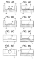
- Figs. 8A to 8H illustrate a variation of the producing method for the liquid discharge head explained with reference to Figs. 5A to 5J and 6A to 6H.
- This variation allows to prepare the liquid path walls 9 and the orifice plate 4 at the same time in the producing method for the liquid discharge head shown in Figs. 5A to 5J and 6A to 6H.
- the producing method for the liquid discharge head in which the liquid path walls 9 and the orifice plate 4 are simultaneously formed.
- Figs. 8A and 8B are cross-sectional views in a direction perpendicular to the extending direction of the liquid path
- Figs. 8C and 8D are elevation views
- Figs. 8E to 8H are cross-sectional views in a direction along the liquid path.
- the SiN film 104 is subjected to photolithographic patterning and etching so as to leave portions thereof corresponding to the liquid path walls 9 and the orifice plate 4, as shown in Figs. 8A and 8E.
- the orifice plate 4 and the liquid path walls 9 of a thickness of 2 to 30 ⁇ m are simultaneously formed on the surface of the element substrate 1.
- the anti-etching protective film 103 on the SiN film 102 is removed by wet etching or dry etching.
- the PSG film 101 under the SiN film 102 is removed with buffered hydrofluoric acid.
- the orifice plate 4 is subjected to ablation by irradiation with an excimer laser, thereby forming the discharge opening 5 in the orifice plate 4.
- the molecular bonding of the SiN film 102 is directly cleaved with a KrF excimer laser having a photon energy of 115 kcal/mol exceeding the dissociation energy of 105 kcal/mol of the SiN film 102.
- the work with the excimer laser being a non-thermal work, can achieve a high precision without thermal deformation or carbonization around the worked part.
- the patterns of the wirings etc. and the position of the through hole to be formed on the element substrate 1 are so determined that the step difference of a height exceeding 1/5 of the thickness of the SiN film 102 is not generated, on the surface of the element substrate 1, in the aforementioned area C, preferably in the area D, defined with respect to the fulcrum of the movable portion of the SiN film 102 (movable member 6), and that the average inclining angle of the entire successive step differences does not exceed 20°.
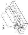
- Fig. 9 is a perspective view of a liquid discharging apparatus in which the above-described liquid discharge head is mounted.
- an ink jet recording apparatus IJRA employing ink as the discharge liquid.
- a carriage HC provided in the apparatus IJRA supports a head cartridge 202 in which a liquid container 90 containing ink and a liquid discharge head 200 are detachably mounted.
- the recording apparatus IJRA is also provided with recording medium conveying means, and the carriage HC reciprocates in the transversal direction (indicated by arrows a, b) of the recording medium 150 such as a recording sheet conveyed by the recording medium conveying means.
- the liquid discharge head 200 discharges ink toward the recording medium 150 in response to such drive signal.
- the recording apparatus IJRA is further provided with a motor 111, gears 112, 113 and carriage shafts 85a, 85b for transmitting the power of the motor 111 to the carriage HC, thereby driving the recording medium conveying means and the carriage HC. Satisfactory recorded images can be obtained by discharging liquid to various recording media by the recording apparatus IJRA.
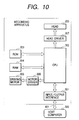
- Fig. 10 is a block diagram of the entire apparatus for driving the ink jet recording apparatus employing the liquid discharge head of the present invention.
- the recording apparatus receives the print infirmation from a host computer 300, as a control signal 401.
- the print information is temporarily stored in an input/output interface 301 in the recording apparatus, and also converted into data processable in the recording apparatus and entered into a CPU 302 serving also as drive signal supply means.
- the CPU 302 processes the data entered thereto, utilizing periphery units such as a RAM 304 and based on a control program stored in a ROM 303, thereby converting the data into print data (image data).
- the CPU 302 prepares data for driving a motor 306 for moving recording sheet and the liquid discharge head 200 in synchronization with the image data, in order to record the image data in an appropriate position on the recording sheet. Simultaneous with the transmission of the image data through the head driver 307 to the liquid discharge head 200, the motor driving data are transmitted to the motor 306 through the motor driver 305. Thus the liquid discharge head 200 and the motor 306 are respectively driven at the controlled timing to form an image.
- the recording medium applicable to the above-described recording apparatus and subjected to deposition of liquid such as ink can be various papers, an OHP sheet, plastic materials employed in the compact disk or decoration plates, cloth, a metal plate such as of aluminum or copper, cow or pig leather, artificial leather, wood or plywood, bamboo, plastics such as a tile, a three-dimensionally structured material such as sponge etc.
- the above-described recording apparatus includes a printer for recording on various papers or OHP sheet; a plastics recording apparatus for recording on plastics such as a compact disk; a metal recording apparatus for recording on metal; a leather recording apparatus for recording on leather; a wood recording apparatus for recording on wood; a ceramic recording apparatus for recording on ceramics; a recording apparatus for recording on a three-dimensionally structure material such as sponge; and a dyeing apparatus for recording on cloth.
- the discharge liquid to be employed in such liquid discharge apparatus can be designed according to respective recording medium and recording conditions.
Landscapes
- Particle Formation And Scattering Control In Inkjet Printers (AREA)
Applications Claiming Priority (2)
| Application Number | Priority Date | Filing Date | Title |
|---|---|---|---|
| JP34473098 | 1998-12-03 | ||
| JP34473098 | 1998-12-03 |
Publications (3)
| Publication Number | Publication Date |
|---|---|
| EP1005992A2 true EP1005992A2 (de) | 2000-06-07 |
| EP1005992A3 EP1005992A3 (de) | 2000-11-29 |
| EP1005992B1 EP1005992B1 (de) | 2006-03-15 |
Family
ID=18371538
Family Applications (1)
| Application Number | Title | Priority Date | Filing Date |
|---|---|---|---|
| EP99309713A Expired - Lifetime EP1005992B1 (de) | 1998-12-03 | 1999-12-02 | Substrat für einen Flüssigkeitsausstosskopf, Flüssigkeitsausstosskopf und Flüssigkeitsausstossgerät |
Country Status (4)
| Country | Link |
|---|---|
| US (1) | US6299293B1 (de) |
| EP (1) | EP1005992B1 (de) |
| AT (1) | ATE320348T1 (de) |
| DE (1) | DE69930358T2 (de) |
Cited By (1)
| Publication number | Priority date | Publication date | Assignee | Title |
|---|---|---|---|---|
| EP2302677A1 (de) * | 2000-12-28 | 2011-03-30 | Canon Kabushiki Kaisha | Herstellungsverfahren für eine Halbleiteranordnung |
Families Citing this family (4)
| Publication number | Priority date | Publication date | Assignee | Title |
|---|---|---|---|---|
| US20060000802A1 (en) * | 2004-06-30 | 2006-01-05 | Ajay Kumar | Method and apparatus for photomask plasma etching |
| TWI426565B (zh) * | 2009-10-15 | 2014-02-11 | 友達光電股份有限公司 | 顯示面板及薄膜電晶體之閘極絕緣層的重工方法 |
| JP6388376B2 (ja) | 2014-06-04 | 2018-09-12 | キヤノン株式会社 | 液体吐出装置 |
| EP3098083B1 (de) | 2015-05-27 | 2021-08-25 | Canon Kabushiki Kaisha | Druckvorrichtung und -platte |
Citations (1)
| Publication number | Priority date | Publication date | Assignee | Title |
|---|---|---|---|---|
| US4723129A (en) | 1977-10-03 | 1988-02-02 | Canon Kabushiki Kaisha | Bubble jet recording method and apparatus in which a heating element generates bubbles in a liquid flow path to project droplets |
Family Cites Families (5)
| Publication number | Priority date | Publication date | Assignee | Title |
|---|---|---|---|---|
| US5278585A (en) | 1992-05-28 | 1994-01-11 | Xerox Corporation | Ink jet printhead with ink flow directing valves |
| JPH08252926A (ja) | 1995-03-17 | 1996-10-01 | Canon Inc | 記録ヘッド及びその記録ヘッドを用いた記録装置 |
| US5821962A (en) * | 1995-06-02 | 1998-10-13 | Canon Kabushiki Kaisha | Liquid ejection apparatus and method |
| DE69733980T2 (de) | 1996-06-07 | 2006-02-23 | Canon K.K. | Verfahren und Vorrichtung zum Ausstossen von Flüssigkeit |
| KR100209498B1 (ko) | 1996-11-08 | 1999-07-15 | 윤종용 | 서로 다른 열팽창 계수 특성을 지닌 다중 멤브레인을 갖는 잉크젯 프린터의 분사장치 |
-
1999
- 1999-12-01 US US09/451,873 patent/US6299293B1/en not_active Expired - Lifetime
- 1999-12-02 DE DE69930358T patent/DE69930358T2/de not_active Expired - Lifetime
- 1999-12-02 AT AT99309713T patent/ATE320348T1/de not_active IP Right Cessation
- 1999-12-02 EP EP99309713A patent/EP1005992B1/de not_active Expired - Lifetime
Patent Citations (1)
| Publication number | Priority date | Publication date | Assignee | Title |
|---|---|---|---|---|
| US4723129A (en) | 1977-10-03 | 1988-02-02 | Canon Kabushiki Kaisha | Bubble jet recording method and apparatus in which a heating element generates bubbles in a liquid flow path to project droplets |
Cited By (1)
| Publication number | Priority date | Publication date | Assignee | Title |
|---|---|---|---|---|
| EP2302677A1 (de) * | 2000-12-28 | 2011-03-30 | Canon Kabushiki Kaisha | Herstellungsverfahren für eine Halbleiteranordnung |
Also Published As
| Publication number | Publication date |
|---|---|
| DE69930358T2 (de) | 2006-11-09 |
| ATE320348T1 (de) | 2006-04-15 |
| DE69930358D1 (de) | 2006-05-11 |
| EP1005992B1 (de) | 2006-03-15 |
| EP1005992A3 (de) | 2000-11-29 |
| US6299293B1 (en) | 2001-10-09 |
Similar Documents
| Publication | Publication Date | Title |
|---|---|---|
| US6439700B1 (en) | Liquid discharge head, liquid discharge method, head cartridge and liquid discharge device | |
| JP2000198199A (ja) | 液体吐出ヘッドおよびヘッドカートリッジおよび液体吐出装置および液体吐出ヘッドの製造方法 | |
| US6468437B1 (en) | Method for producing liquid discharging head | |
| JP3927711B2 (ja) | 液体吐出ヘッドの製造方法 | |
| US6378993B1 (en) | Liquid discharge head, producing method therefor and liquid discharge apparatus | |
| EP1080902B1 (de) | Flüssigkeitsausstosskopf, Flüssigkeitsausstossapparat und Flüssigkeitsausstossverfahren | |
| EP1005992B1 (de) | Substrat für einen Flüssigkeitsausstosskopf, Flüssigkeitsausstosskopf und Flüssigkeitsausstossgerät | |
| US6302518B1 (en) | Liquid discharging head, liquid discharging apparatus and printing system | |
| JP3235260B2 (ja) | インクジェットヘッド | |
| JP3548536B2 (ja) | 液体吐出ヘッドの製造方法 | |
| EP0894628B1 (de) | Flüssigkeitsausstossverfahren, Flüssigkeitsausstosskopf, Kopfkassette und Flüssigkeitsausstossapparat welcher diesen Flüssigkeitsausstosskopf verwendet | |
| US6474792B2 (en) | Liquid discharge head, method for manufacturing liquid discharge head, head cartridge on which liquid discharge head is mounted, and liquid discharge apparatus | |
| EP1005993B1 (de) | Flüssigkeitsausstosskopf und Flüssigkeitsausstossgerät | |
| EP1188563B1 (de) | Flüssigkeitsausstosskopf, Flüssigkeitsausstossapparat sowie Verfahren zur Herstellung des Flüssigkeitsausstosskopfes | |
| JP3862524B2 (ja) | 液体吐出ヘッド、液体吐出装置、および液体吐出ヘッドの製造方法 | |
| JP2000225705A (ja) | 液体吐出ヘッド用基板、液体吐出ヘッド、及び液体吐出装置 | |
| EP0921004A2 (de) | Flüssigkeitsausstosskopf , Aufzeichnungsgerät und Flüssigkeitsausstosskopfenherstellungsverfahren | |
| AU775428B2 (en) | Liquid discharging head, liquid discharging apparatus and printing system | |
| JP3347590B2 (ja) | 液体吐出ヘッド、ヘッドカートリッジ及び液体吐出装置 | |
| JPH11235828A (ja) | 液体吐出ヘッド、液体吐出方法、ヘッドカートリッジおよび液体吐出装置 | |
| JP2000225711A (ja) | 液体吐出ヘッドの製造方法 | |
| JP2001179994A (ja) | 液体吐出ヘッドの製造方法、液体吐出ヘッド、液体吐出ヘッドカートリッジおよび液体吐出装置 | |
| JPH1024589A (ja) | 液体吐出ヘッド、および、その製造方法 | |
| JP2000225706A (ja) | 液体吐出ヘッドおよびその製造方法と液体吐出装置 | |
| JPH1148500A (ja) | 液体吐出ヘッド用可動部材及びそれの製造方法とそれを有する液体吐出ヘッド |
Legal Events
| Date | Code | Title | Description |
|---|---|---|---|
| PUAI | Public reference made under article 153(3) epc to a published international application that has entered the european phase |
Free format text: ORIGINAL CODE: 0009012 |
|
| AK | Designated contracting states |
Kind code of ref document: A2 Designated state(s): AT BE CH CY DE DK ES FI FR GB GR IE IT LI LU MC NL PT SE |
|
| AX | Request for extension of the european patent |
Free format text: AL;LT;LV;MK;RO;SI |
|
| PUAL | Search report despatched |
Free format text: ORIGINAL CODE: 0009013 |
|
| AK | Designated contracting states |
Kind code of ref document: A3 Designated state(s): AT BE CH CY DE DK ES FI FR GB GR IE IT LI LU MC NL PT SE |
|
| AX | Request for extension of the european patent |
Free format text: AL;LT;LV;MK;RO;SI |
|
| 17P | Request for examination filed |
Effective date: 20010411 |
|
| AKX | Designation fees paid |
Free format text: AT BE CH CY DE DK ES FI FR GB GR IE IT LI LU MC NL PT SE |
|
| 17Q | First examination report despatched |
Effective date: 20040507 |
|
| GRAP | Despatch of communication of intention to grant a patent |
Free format text: ORIGINAL CODE: EPIDOSNIGR1 |
|
| GRAS | Grant fee paid |
Free format text: ORIGINAL CODE: EPIDOSNIGR3 |
|
| GRAA | (expected) grant |
Free format text: ORIGINAL CODE: 0009210 |
|
| AK | Designated contracting states |
Kind code of ref document: B1 Designated state(s): AT BE CH CY DE DK ES FI FR GB GR IE IT LI LU MC NL PT SE |
|
| PG25 | Lapsed in a contracting state [announced via postgrant information from national office to epo] |
Ref country code: NL Free format text: LAPSE BECAUSE OF FAILURE TO SUBMIT A TRANSLATION OF THE DESCRIPTION OR TO PAY THE FEE WITHIN THE PRESCRIBED TIME-LIMIT Effective date: 20060315 Ref country code: LI Free format text: LAPSE BECAUSE OF FAILURE TO SUBMIT A TRANSLATION OF THE DESCRIPTION OR TO PAY THE FEE WITHIN THE PRESCRIBED TIME-LIMIT Effective date: 20060315 Ref country code: FI Free format text: LAPSE BECAUSE OF FAILURE TO SUBMIT A TRANSLATION OF THE DESCRIPTION OR TO PAY THE FEE WITHIN THE PRESCRIBED TIME-LIMIT Effective date: 20060315 Ref country code: CH Free format text: LAPSE BECAUSE OF FAILURE TO SUBMIT A TRANSLATION OF THE DESCRIPTION OR TO PAY THE FEE WITHIN THE PRESCRIBED TIME-LIMIT Effective date: 20060315 Ref country code: BE Free format text: LAPSE BECAUSE OF FAILURE TO SUBMIT A TRANSLATION OF THE DESCRIPTION OR TO PAY THE FEE WITHIN THE PRESCRIBED TIME-LIMIT Effective date: 20060315 Ref country code: AT Free format text: LAPSE BECAUSE OF FAILURE TO SUBMIT A TRANSLATION OF THE DESCRIPTION OR TO PAY THE FEE WITHIN THE PRESCRIBED TIME-LIMIT Effective date: 20060315 |
|
| REG | Reference to a national code |
Ref country code: GB Ref legal event code: FG4D Ref country code: CH Ref legal event code: EP |
|
| REG | Reference to a national code |
Ref country code: IE Ref legal event code: FG4D |
|
| REF | Corresponds to: |
Ref document number: 69930358 Country of ref document: DE Date of ref document: 20060511 Kind code of ref document: P |
|
| PG25 | Lapsed in a contracting state [announced via postgrant information from national office to epo] |
Ref country code: SE Free format text: LAPSE BECAUSE OF FAILURE TO SUBMIT A TRANSLATION OF THE DESCRIPTION OR TO PAY THE FEE WITHIN THE PRESCRIBED TIME-LIMIT Effective date: 20060615 Ref country code: DK Free format text: LAPSE BECAUSE OF FAILURE TO SUBMIT A TRANSLATION OF THE DESCRIPTION OR TO PAY THE FEE WITHIN THE PRESCRIBED TIME-LIMIT Effective date: 20060615 |
|
| PG25 | Lapsed in a contracting state [announced via postgrant information from national office to epo] |
Ref country code: ES Free format text: LAPSE BECAUSE OF FAILURE TO SUBMIT A TRANSLATION OF THE DESCRIPTION OR TO PAY THE FEE WITHIN THE PRESCRIBED TIME-LIMIT Effective date: 20060626 |
|
| PG25 | Lapsed in a contracting state [announced via postgrant information from national office to epo] |
Ref country code: PT Free format text: LAPSE BECAUSE OF FAILURE TO SUBMIT A TRANSLATION OF THE DESCRIPTION OR TO PAY THE FEE WITHIN THE PRESCRIBED TIME-LIMIT Effective date: 20060816 |
|
| NLV1 | Nl: lapsed or annulled due to failure to fulfill the requirements of art. 29p and 29m of the patents act | ||
| REG | Reference to a national code |
Ref country code: CH Ref legal event code: PL |
|
| ET | Fr: translation filed | ||
| PG25 | Lapsed in a contracting state [announced via postgrant information from national office to epo] |
Ref country code: IE Free format text: LAPSE BECAUSE OF NON-PAYMENT OF DUE FEES Effective date: 20061204 |
|
| PG25 | Lapsed in a contracting state [announced via postgrant information from national office to epo] |
Ref country code: MC Free format text: LAPSE BECAUSE OF NON-PAYMENT OF DUE FEES Effective date: 20061231 |
|
| PLBE | No opposition filed within time limit |
Free format text: ORIGINAL CODE: 0009261 |
|
| STAA | Information on the status of an ep patent application or granted ep patent |
Free format text: STATUS: NO OPPOSITION FILED WITHIN TIME LIMIT |
|
| 26N | No opposition filed |
Effective date: 20061218 |
|
| PG25 | Lapsed in a contracting state [announced via postgrant information from national office to epo] |
Ref country code: GR Free format text: LAPSE BECAUSE OF FAILURE TO SUBMIT A TRANSLATION OF THE DESCRIPTION OR TO PAY THE FEE WITHIN THE PRESCRIBED TIME-LIMIT Effective date: 20060616 |
|
| PG25 | Lapsed in a contracting state [announced via postgrant information from national office to epo] |
Ref country code: LU Free format text: LAPSE BECAUSE OF NON-PAYMENT OF DUE FEES Effective date: 20061202 |
|
| PG25 | Lapsed in a contracting state [announced via postgrant information from national office to epo] |
Ref country code: CY Free format text: LAPSE BECAUSE OF FAILURE TO SUBMIT A TRANSLATION OF THE DESCRIPTION OR TO PAY THE FEE WITHIN THE PRESCRIBED TIME-LIMIT Effective date: 20060315 |
|
| PGFP | Annual fee paid to national office [announced via postgrant information from national office to epo] |
Ref country code: IT Payment date: 20081211 Year of fee payment: 10 |
|
| PGFP | Annual fee paid to national office [announced via postgrant information from national office to epo] |
Ref country code: FR Payment date: 20081222 Year of fee payment: 10 |
|
| REG | Reference to a national code |
Ref country code: FR Ref legal event code: ST Effective date: 20100831 |
|
| PG25 | Lapsed in a contracting state [announced via postgrant information from national office to epo] |
Ref country code: FR Free format text: LAPSE BECAUSE OF NON-PAYMENT OF DUE FEES Effective date: 20091231 |
|
| PG25 | Lapsed in a contracting state [announced via postgrant information from national office to epo] |
Ref country code: IT Free format text: LAPSE BECAUSE OF NON-PAYMENT OF DUE FEES Effective date: 20091202 |
|
| PGFP | Annual fee paid to national office [announced via postgrant information from national office to epo] |
Ref country code: GB Payment date: 20151218 Year of fee payment: 17 |
|
| PGFP | Annual fee paid to national office [announced via postgrant information from national office to epo] |
Ref country code: DE Payment date: 20151231 Year of fee payment: 17 |
|
| REG | Reference to a national code |
Ref country code: DE Ref legal event code: R119 Ref document number: 69930358 Country of ref document: DE |
|
| GBPC | Gb: european patent ceased through non-payment of renewal fee |
Effective date: 20161202 |
|
| PG25 | Lapsed in a contracting state [announced via postgrant information from national office to epo] |
Ref country code: GB Free format text: LAPSE BECAUSE OF NON-PAYMENT OF DUE FEES Effective date: 20161202 Ref country code: DE Free format text: LAPSE BECAUSE OF NON-PAYMENT OF DUE FEES Effective date: 20170701 |