EP1006450B1 - Appareil de transfert bidirectionnel de signaux - Google Patents
Appareil de transfert bidirectionnel de signaux Download PDFInfo
- Publication number
- EP1006450B1 EP1006450B1 EP19990123482 EP99123482A EP1006450B1 EP 1006450 B1 EP1006450 B1 EP 1006450B1 EP 19990123482 EP19990123482 EP 19990123482 EP 99123482 A EP99123482 A EP 99123482A EP 1006450 B1 EP1006450 B1 EP 1006450B1
- Authority
- EP
- European Patent Office
- Prior art keywords
- signal
- arbitration
- transceiver
- absolute
- absolute signal
- Prior art date
- Legal status (The legal status is an assumption and is not a legal conclusion. Google has not performed a legal analysis and makes no representation as to the accuracy of the status listed.)
- Expired - Lifetime
Links
Images
Classifications
-
- G—PHYSICS
- G06—COMPUTING OR CALCULATING; COUNTING
- G06F—ELECTRIC DIGITAL DATA PROCESSING
- G06F13/00—Interconnection of, or transfer of information or other signals between, memories, input/output devices or central processing units
- G06F13/38—Information transfer, e.g. on bus
- G06F13/42—Bus transfer protocol, e.g. handshake; Synchronisation
- G06F13/4265—Bus transfer protocol, e.g. handshake; Synchronisation on a point to point bus
- G06F13/4278—Bus transfer protocol, e.g. handshake; Synchronisation on a point to point bus using an embedded synchronisation
-
- G—PHYSICS
- G06—COMPUTING OR CALCULATING; COUNTING
- G06F—ELECTRIC DIGITAL DATA PROCESSING
- G06F13/00—Interconnection of, or transfer of information or other signals between, memories, input/output devices or central processing units
- G06F13/14—Handling requests for interconnection or transfer
- G06F13/20—Handling requests for interconnection or transfer for access to input/output bus
Definitions
- the invention relates to a device for bidirectional signal transmission according to the preamble of the independent claim.
- additional transmitters and receivers are offered, which are connected to each other via a cable of up to 300 m in length.
- the influence of the cable length can be adjusted individually on the transmitter.
- microprocessors are necessary, so that such systems are relatively complex and therefore expensive.
- the device according to the invention for bidirectional signal transmission between a computer and a peripheral device has an arbitration logic for monitoring and influencing the access authorization to at least one signal transmission line.
- a likewise provided transceiver converts at least one absolute signal into differential signals.
- the arbitration logic receives or outputs the at least one absolute signal via the absolute signal transmission line.
- the arbitration logic outputs at least one arbitration output to the transceiver.
- the transceiver supplies at least one arbitration input signal to the arbitration logic. Thanks to the arbitration logic data collisions, which could arise due to a bidirectional standard connection between the computer and the periphery avoided, since the arbitration logic in the present data transfer in one direction does not allow a data transfer in the other direction.
- In a differential signal and the reference potential is carried on a second signal transmission line.
- Interference occurs in both differential signals in the same way and can be eliminated after the transmission path by means of a subtractive superposition of the two differential signals.
- the conversion of the absolute signal into a differential signal and vice versa by the transceiver allows the transmission of interference-susceptible differential signal even over long transmission paths.
- the transceiver can be used on a standard block, which is used for example in the networking of vehicle control units via a bus system.
- the arbitration logic can be realized as pure hardware solutions without the need for special processors.
- the device according to the invention for bidirectional signal transmission contributes to an increase in transmission reliability at low production costs.
- arbitration logic and transceivers are integrated into an assembly.
- the electronic components can preferably be arranged on a circuit board. This allows this module as Insert plug-in card easily into the computer or the periphery.
- the absolute signal is supplied to a Schmitt trigger whose output signal is passed to the Arbitr istslogik. This avoids unstable states in the arbitration logic. The susceptibility of the device according to the invention can thereby be reduced.
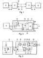
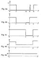
- FIG. 1 a block diagram, the FIGS. 2 and 3 possible circuitry implementations as well as the FIGS. 4a-4e possible signal waveforms of the embodiment.
- a computer 10 exchanges an absolute signal 46 with a signal processor 12 via an absolute signal transmission line 16.
- the signal processing 12 is connected via a two-wire differential signal transmission line 18 with a further, identically constructed signal processing 12. Via the differential signal transmission line 18, a first differential signal 48 and a second differential signal 50 are transmitted bidirectionally.
- the further signal processing 12 via a further absolute signal transmission line 16 for Exchange of a bidirectional absolute signal 46 connected to a peripheral 14.
- the signal processing 12 is shown in its basic operation.
- the bidirectional data exchange with the computer 10 via the absolute signal transmission line 16 ensuring absolute signal 46 is applied to the first input of a first OR gate 41.
- the output of the first OR gate 41 is supplied as an arbitration output signal 52 to a transceiver 35 and a second inverter 44.
- a second OR gate 43 receives, as input, firstly the output signal of the second inverter 44 and an arbitration input signal 54 provided by the transceiver 35.
- the output signal of the second OR gate 43 is applied via a first inverter 42 to the second input of the first OR gate 41 laid.
- the output signal of the second OR gate 43 of the absolute transmission line 16 can be supplied as to be sent to the computer 10 absolute signal 46.
- the transmitter 35 transmits / receives the first and second differential signals 48, 50, which are carried in a two-wire differential signal transmission line 18.
- a transmit transistor 21 is typified, which outputs the signal generated by the computer 10 as an absolute signal 46 to the absolute signal transmission line 16.
- An absolute signal 16 to be received is supplied via a receiving amplifier 23 to a further evaluation unit.
- the absolute signal 46 is applied to the input of a Schmitt-Triggers 25 placed. Its inverting output is an input of an AND gate 27.
- the inverted output of the AND gate 27 serves as an input to a first D flip-flop 29.
- the output of the first D flip-flop 29 serves the transceiver 35 as an input.
- the inverting output of the first D flip-flop 29 serves as an OR gate 33 as a first input.
- the transceiver 35 provides the second input to the OR gate 33.
- the output of the OR gate 33 is supplied to a second D flip-flop 31 as an input. Its output is applied to the input of the AND gate 27. From the inverting output of the second D flip-flop 31, a further transistor is driven. About this transistor, the absolute signal 16 can be generated.
- FIG. 1 proposed basic arrangement is used for interference-proof bidirectional transmission of the absolute signal 46 between the computer 10 and the periphery 14.
- the computer 10 may be a personal computer to be controlled in a known manner via keyboard and mouse as a peripheral 14. Between computer 10 and peripheral 14 is a long distance to overcome, which would be possible with a conventional absolute signal 46 only with great disturbances at the expense of data security.
- a peripheral 14 for example, a screen could be used.
- the Arbitr istslogik 20 arranged in the signal processing 12 ensures that in a transmission process of the computer 10 from the periphery 14 no data can be given to the absolute signal transmission line 16.
- the data transmission in the direction of the computer 10 is only released when the arbitration logic 20 the end of the transmission of the Calculator 10 has detected.
- the absolute signal 46 is an open-collector signal, which is provided by default for data exchange between personal computer and keyboard, for example. The high level could be reached at a voltage level of 5 volts.
- This absolute signal 46 converts the transceiver 35 into two differential signals 48, 50. In this case, the reference potential of the first differential signal 48 is additionally transmitted as a second differential signal 50. Any perturbations of the differential signal transmission line 18 will affect the two differential signals 48, 50 in the same manner.
- the reconversion of the differential signals 48, 50 into the absolute signal 46 takes place by subtraction. As a result, the interference is eliminated, so that the resulting absolute signal 46 has no interference that might otherwise have occurred, for example, in the course of the long transmission path.
- a transceiver 35 for example, a so-called CAN bus transceiver is used, which converts the absolute signal 46 and the differential signals 48, 50 to use the familiar in the automotive industry CAN bus.
- FIG. 1 shown arrangement can be extended according to the number of signals to be transmitted such as keyboard signal, mouse signal, clock signal accordingly. However, nothing changes in the basic functionality.
- the computer 10 does not send and receive data via the absolute signal transmission line 16.
- the absolute signal 46 assumes the value Logic 1.
- the computer 10 sends data to the periphery 14.
- the in FIG. 3 shown transmit transistor 21 is driven, so that the absolute signal 46 assumes the value logic 0.
- the transceiver 35 outputs an arbitration signal 54 having the logic 1 state to the second OR gate 43. Its output signal always assumes the logic 1 state.
- the signal with the state logic 0 inverted via the first inverter 42 is applied to the one input of the first OR gate 41.
- the absolute signal 46 of the state Logical 1 in the state logical 0 time T1
- the output of the first OR gate 41 changes from logic 1 to logic 0, which corresponds to the arbitration output 52.
- the transceiver 35 converts this arbitration output signal 52 into a differential signal 48, 50.
- the Arbitr istsausgangssignal 52 assumes the state logic 0 - the computer 10 is the authorization granted as a sender - may have a successful transmission of the peripheral 14, the absolute signal transmission line 16 is not affected.
- a Schmitt trigger 25 which converts a possibly flat rising edge of the absolute signal 16 into a square wave signal.
- the D flip-flops 29, 31 are acted upon by a clock, not shown, and take over at each clock the meanwhile pending input signal.
- the monitoring of the input signals of the arbitration logic 20, namely the absolute signal 46 and the arbitration input signal 54 always follows alternately with the clock.
- the absolute signal 46 At the first clock time, the absolute signal 46, at the second clock time the Arbitr istseingangssignal 54, at the third clock time in turn, the absolute signal 46 monitors, etc. ..
- the periphery sends 14 and the arbitration logic 20 of the periphery 14 has also given the transmission permission for the absolute signal transmission line 16 , the signal 0 at the output of the OR gate 33 is inverted in order to drive the transmit transistor. This causes the signal change of the absolute signal 46 to logic 0.
- Preferred use is the device according to the invention for computer systems in industrial use, in which the computers are arranged at the periphery 14 further away points.
- the device described prevents data collisions and allows interference-free data transmission from and to the described computer peripherals.
Landscapes
- Engineering & Computer Science (AREA)
- Theoretical Computer Science (AREA)
- Physics & Mathematics (AREA)
- General Engineering & Computer Science (AREA)
- General Physics & Mathematics (AREA)
- Bidirectional Digital Transmission (AREA)
- Dc Digital Transmission (AREA)
Claims (7)
- Dispositif pour la transmission bidirectionnelle de signaux entre un calculateur (10) et un périphérique (14) comportant une logique d'arbitrage (20) pour surveiller et influencer l'autorisation d'accès à au moins un ligne de transmission de signaux (16, 18), un émetteur-récepteur (35) qui convertit un signal absolu (16) en au moins un signal différentiel (48, 50),
la logique d'arbitrage (20) recevant au moins un signal absolu (46) par la ligne de transmission de signaux absolus (16) ou envoyant un tel signal, la logique d'arbitrage (20) émettant au moins un signal de sortie d'arbitrage (52) vers le récepteur-émetteur (35) et le récepteur-émetteur (35) fournit à la logique d'arbitrage (20) au moins un signal d'entrée d'arbitrage (54). - Dispositif selon la revendication 1,
caractérisé en ce que
la logique d'arbitrage (20) comprend des moyens qui, pour un signal absolu (46) d'entrée, correspondant à une transmission de données, ne transmettent pas le signal d'entrée d'arbitrage (54) à la ligne de transmission de signaux absolus (16). - Dispositif selon l'une des revendications précédentes,
caractérisé en ce que
la logique d'arbitrage (20) comporte des moyens qui, pour un signal d'entrée d'arbitrage (54) correspondant à une transmission, fournissent un signal de sortie d'arbitrage (52) correspondant à une transmission de données vers le récepteur-émetteur (35). - Dispositif selon l'une des revendications précédentes,
caractérisé en ce que
la logique d'arbitrage (20) et le récepteur-émetteur (35) sont intégrés dans un ensemble. - Dispositif selon l'une des revendications précédentes,
caractérisé en ce que
le signal absolu (46) est fourni à un déclencheur de Schmitt (25). - Dispositif selon l'une des revendications précédentes,
caractérisé en ce que
l'émetteur-récepteur (35) réalise la conversion de signaux absolus (46) en signaux différentiels (48, 50) et inversement en liaison avec un protocole de bus. - Dispositif selon l'une des revendications précédentes,
caractérisé en ce qu'
un calculateur est relié par une ligne de signaux absolus (16) à une logique d'arbitrage (20) qui échange les signaux avec le récepteur-émetteur (35) et au moins une ligne de transmission de signaux différentiels (18) est prévue vers un autre récepteur-émetteur qui échange les signaux avec une autre logique d'arbitrage et celle-ci échange des données par une autre ligne de transmission de signaux absolus avec le périphérique (14).
Applications Claiming Priority (2)
| Application Number | Priority Date | Filing Date | Title |
|---|---|---|---|
| DE19855372 | 1998-12-01 | ||
| DE1998155372 DE19855372A1 (de) | 1998-12-01 | 1998-12-01 | Vorrichtung zur bidirektionalen Signalübertragung |
Publications (3)
| Publication Number | Publication Date |
|---|---|
| EP1006450A2 EP1006450A2 (fr) | 2000-06-07 |
| EP1006450A3 EP1006450A3 (fr) | 2004-12-22 |
| EP1006450B1 true EP1006450B1 (fr) | 2008-09-03 |
Family
ID=7889611
Family Applications (1)
| Application Number | Title | Priority Date | Filing Date |
|---|---|---|---|
| EP19990123482 Expired - Lifetime EP1006450B1 (fr) | 1998-12-01 | 1999-11-25 | Appareil de transfert bidirectionnel de signaux |
Country Status (3)
| Country | Link |
|---|---|
| EP (1) | EP1006450B1 (fr) |
| DE (2) | DE19855372A1 (fr) |
| ES (1) | ES2310934T3 (fr) |
Family Cites Families (2)
| Publication number | Priority date | Publication date | Assignee | Title |
|---|---|---|---|---|
| JPS60252979A (ja) * | 1984-05-30 | 1985-12-13 | Oki Electric Ind Co Ltd | Cmos入出力回路 |
| JP3557625B2 (ja) * | 1993-08-06 | 2004-08-25 | ブラザー工業株式会社 | 情報処理装置 |
-
1998
- 1998-12-01 DE DE1998155372 patent/DE19855372A1/de not_active Ceased
-
1999
- 1999-11-25 DE DE59914862T patent/DE59914862D1/de not_active Expired - Lifetime
- 1999-11-25 EP EP19990123482 patent/EP1006450B1/fr not_active Expired - Lifetime
- 1999-11-25 ES ES99123482T patent/ES2310934T3/es not_active Expired - Lifetime
Also Published As
| Publication number | Publication date |
|---|---|
| DE19855372A1 (de) | 2000-06-08 |
| ES2310934T3 (es) | 2009-01-16 |
| EP1006450A3 (fr) | 2004-12-22 |
| DE59914862D1 (de) | 2008-10-16 |
| EP1006450A2 (fr) | 2000-06-07 |
Similar Documents
| Publication | Publication Date | Title |
|---|---|---|
| DE69428885T2 (de) | Ein kommunikationsknotenpunkt mit einer ersten buskonfiguration für arbitrierung und einer zweiten buskonfiguration für datenübertragung | |
| DE102009027625A1 (de) | Elektrische Schaltung zur Übertragung von Signalen zwischen zwei Mastern und einem oder mehreren Slaves | |
| DE102017218134B3 (de) | Verfahren und Vorrichtung zum Übertragen einer Botschaftsfolge über einen Datenbus sowie Verfahren und Vorrichtung zum Erkennen eines Angriffs auf eine so übertragene Botschaftsfolge | |
| DE19833693C2 (de) | Schnittstelle für I·2·C-Bus | |
| EP1227406B1 (fr) | Dispositif d'émission et de réception avec des moyens de gestion d'erreur | |
| DE3687047T2 (de) | Uebertragungsschaltung. | |
| DE112021004851T5 (de) | Bidirektionale Kommunikationsschaltung und Verfahren zum Betreiben einer bidirektionalen Kommunikationsschaltung | |
| DE69222336T2 (de) | Steuerungsschaltung für Halbduplex-Simplexschnittstelle in einem Übertragungssystem | |
| EP1006450A2 (fr) | Appareil de transfert bidirectionnel de signaux | |
| DE4005087C1 (en) | Connector unit for domestic power installation - has adaptor for specific function allowing data transmission via bus and data lines | |
| DE10141040B4 (de) | Serielle Schnittstelleneinheit | |
| DE102019116657A1 (de) | System und Verfahren zur kombinierten Energieübertragung und Datenübertragung in einem Automatisierungssystem | |
| EP2452467B1 (fr) | Dispositif de transmission de signaux et composant de véhicule | |
| DE102008062994B4 (de) | Messanordnung | |
| WO2020069818A1 (fr) | Procédé de transmission d'au moins un signal utile entre deux unités émettrices/réceptrices, unité émettrice/réceptrice et véhicule | |
| DE10239846B4 (de) | Fail-Silent-Steuergerät | |
| EP1193131A1 (fr) | Vehicule avec plusieurs modules sans fil | |
| DE10056532B4 (de) | Verfahren zur manipulationsgeschützten Datenkommunikation | |
| DE102008064896B3 (de) | Messanordnung | |
| EP3087460B1 (fr) | Procédé, dispositif et système pour une communication avec un capteur | |
| DE102012201669B4 (de) | Verfahren und Kommunikationscontroller zur Datenübertragung zwischen zwei mittels Übertragungsstrecken verbundenen Datenverarbeitungseinheiten | |
| DE102009043629A1 (de) | Serielle Busstruktur | |
| DE102010044993A1 (de) | Verfahren zur Datenübertragung und Vorrichtung zur Umfelderfassung | |
| WO2000027078A1 (fr) | Procede et dispositif pour verifier la fonction de blocage d'un dispositif de blocage de transmission de constituants de reseau | |
| DE2532984C3 (de) | Schaltungsanordnung zum Überwachen einer Nahtstelle zwischen Steuereinheiten |
Legal Events
| Date | Code | Title | Description |
|---|---|---|---|
| PUAI | Public reference made under article 153(3) epc to a published international application that has entered the european phase |
Free format text: ORIGINAL CODE: 0009012 |
|
| AK | Designated contracting states |
Kind code of ref document: A2 Designated state(s): AT BE CH CY DE DK ES FI FR GB GR IE IT LI LU MC NL PT SE |
|
| AX | Request for extension of the european patent |
Free format text: AL;LT;LV;MK;RO;SI |
|
| PUAL | Search report despatched |
Free format text: ORIGINAL CODE: 0009013 |
|
| AK | Designated contracting states |
Kind code of ref document: A3 Designated state(s): AT BE CH CY DE DK ES FI FR GB GR IE IT LI LU MC NL PT SE |
|
| AX | Request for extension of the european patent |
Extension state: AL LT LV MK RO SI |
|
| 17P | Request for examination filed |
Effective date: 20050622 |
|
| AKX | Designation fees paid |
Designated state(s): CH DE ES IT LI |
|
| GRAP | Despatch of communication of intention to grant a patent |
Free format text: ORIGINAL CODE: EPIDOSNIGR1 |
|
| GRAS | Grant fee paid |
Free format text: ORIGINAL CODE: EPIDOSNIGR3 |
|
| GRAA | (expected) grant |
Free format text: ORIGINAL CODE: 0009210 |
|
| AK | Designated contracting states |
Kind code of ref document: B1 Designated state(s): CH DE ES IT LI |
|
| REG | Reference to a national code |
Ref country code: CH Ref legal event code: EP |
|
| REG | Reference to a national code |
Ref country code: CH Ref legal event code: NV Representative=s name: SCINTILLA AG, DIREKTION |
|
| REF | Corresponds to: |
Ref document number: 59914862 Country of ref document: DE Date of ref document: 20081016 Kind code of ref document: P |
|
| REG | Reference to a national code |
Ref country code: ES Ref legal event code: FG2A Ref document number: 2310934 Country of ref document: ES Kind code of ref document: T3 |
|
| PGFP | Annual fee paid to national office [announced via postgrant information from national office to epo] |
Ref country code: CH Payment date: 20081124 Year of fee payment: 10 |
|
| PGFP | Annual fee paid to national office [announced via postgrant information from national office to epo] |
Ref country code: ES Payment date: 20081121 Year of fee payment: 10 |
|
| PGFP | Annual fee paid to national office [announced via postgrant information from national office to epo] |
Ref country code: IT Payment date: 20081127 Year of fee payment: 10 |
|
| PLBE | No opposition filed within time limit |
Free format text: ORIGINAL CODE: 0009261 |
|
| STAA | Information on the status of an ep patent application or granted ep patent |
Free format text: STATUS: NO OPPOSITION FILED WITHIN TIME LIMIT |
|
| 26N | No opposition filed |
Effective date: 20090604 |
|
| PGFP | Annual fee paid to national office [announced via postgrant information from national office to epo] |
Ref country code: DE Payment date: 20100121 Year of fee payment: 11 |
|
| REG | Reference to a national code |
Ref country code: CH Ref legal event code: PL |
|
| PG25 | Lapsed in a contracting state [announced via postgrant information from national office to epo] |
Ref country code: LI Free format text: LAPSE BECAUSE OF NON-PAYMENT OF DUE FEES Effective date: 20091130 Ref country code: CH Free format text: LAPSE BECAUSE OF NON-PAYMENT OF DUE FEES Effective date: 20091130 |
|
| REG | Reference to a national code |
Ref country code: ES Ref legal event code: FD2A Effective date: 20110329 |
|
| PG25 | Lapsed in a contracting state [announced via postgrant information from national office to epo] |
Ref country code: IT Free format text: LAPSE BECAUSE OF NON-PAYMENT OF DUE FEES Effective date: 20091125 |
|
| PG25 | Lapsed in a contracting state [announced via postgrant information from national office to epo] |
Ref country code: ES Free format text: LAPSE BECAUSE OF NON-PAYMENT OF DUE FEES Effective date: 20110316 |
|
| PG25 | Lapsed in a contracting state [announced via postgrant information from national office to epo] |
Ref country code: ES Free format text: LAPSE BECAUSE OF NON-PAYMENT OF DUE FEES Effective date: 20091126 Ref country code: DE Free format text: LAPSE BECAUSE OF NON-PAYMENT OF DUE FEES Effective date: 20110531 |
|
| REG | Reference to a national code |
Ref country code: DE Ref legal event code: R119 Ref document number: 59914862 Country of ref document: DE Effective date: 20110601 Ref country code: DE Ref legal event code: R119 Ref document number: 59914862 Country of ref document: DE Effective date: 20110531 |