EP1006571A2 - Procédé d'un dispositif semiconducteur avec une meilleure couverture en gradins de contacts sans sacrifier la fiabilité des linéaires d'aluminium - Google Patents
Procédé d'un dispositif semiconducteur avec une meilleure couverture en gradins de contacts sans sacrifier la fiabilité des linéaires d'aluminium Download PDFInfo
- Publication number
- EP1006571A2 EP1006571A2 EP99123516A EP99123516A EP1006571A2 EP 1006571 A2 EP1006571 A2 EP 1006571A2 EP 99123516 A EP99123516 A EP 99123516A EP 99123516 A EP99123516 A EP 99123516A EP 1006571 A2 EP1006571 A2 EP 1006571A2
- Authority
- EP
- European Patent Office
- Prior art keywords
- temperature
- layer
- aluminum
- insulating layer
- set forth
- Prior art date
- Legal status (The legal status is an assumption and is not a legal conclusion. Google has not performed a legal analysis and makes no representation as to the accuracy of the status listed.)
- Ceased
Links
Images



Classifications
-
- H—ELECTRICITY
- H10—SEMICONDUCTOR DEVICES; ELECTRIC SOLID-STATE DEVICES NOT OTHERWISE PROVIDED FOR
- H10P—GENERIC PROCESSES OR APPARATUS FOR THE MANUFACTURE OR TREATMENT OF DEVICES COVERED BY CLASS H10
- H10P50/00—Etching of wafers, substrates or parts of devices
-
- H—ELECTRICITY
- H10—SEMICONDUCTOR DEVICES; ELECTRIC SOLID-STATE DEVICES NOT OTHERWISE PROVIDED FOR
- H10W—GENERIC PACKAGES, INTERCONNECTIONS, CONNECTORS OR OTHER CONSTRUCTIONAL DETAILS OF DEVICES COVERED BY CLASS H10
- H10W20/00—Interconnections in chips, wafers or substrates
- H10W20/01—Manufacture or treatment
- H10W20/071—Manufacture or treatment of dielectric parts thereof
- H10W20/081—Manufacture or treatment of dielectric parts thereof by forming openings in the dielectric parts
- H10W20/082—Manufacture or treatment of dielectric parts thereof by forming openings in the dielectric parts the openings being tapered via holes
-
- H—ELECTRICITY
- H10—SEMICONDUCTOR DEVICES; ELECTRIC SOLID-STATE DEVICES NOT OTHERWISE PROVIDED FOR
- H10W—GENERIC PACKAGES, INTERCONNECTIONS, CONNECTORS OR OTHER CONSTRUCTIONAL DETAILS OF DEVICES COVERED BY CLASS H10
- H10W20/00—Interconnections in chips, wafers or substrates
- H10W20/01—Manufacture or treatment
- H10W20/031—Manufacture or treatment of conductive parts of the interconnections
- H10W20/056—Manufacture or treatment of conductive parts of the interconnections by filling conductive material into holes, grooves or trenches
-
- H—ELECTRICITY
- H10—SEMICONDUCTOR DEVICES; ELECTRIC SOLID-STATE DEVICES NOT OTHERWISE PROVIDED FOR
- H10W—GENERIC PACKAGES, INTERCONNECTIONS, CONNECTORS OR OTHER CONSTRUCTIONAL DETAILS OF DEVICES COVERED BY CLASS H10
- H10W20/00—Interconnections in chips, wafers or substrates
- H10W20/01—Manufacture or treatment
- H10W20/071—Manufacture or treatment of dielectric parts thereof
- H10W20/093—Manufacture or treatment of dielectric parts thereof by modifying materials of the dielectric parts
- H10W20/097—Manufacture or treatment of dielectric parts thereof by modifying materials of the dielectric parts by thermally treating
Definitions
- This invention relates to a fabrication technology for a semiconductor device and, more particularly, to a process for fabricating a semiconductor device having via holes.
- a large number of circuit components are fabricated on a single semiconductor chip, and form an integrated circuit device.
- the integrated circuit has been complicated, and, accordingly, the circuit components have been increased.
- a multi- layered wiring structure is required for the integrated circuit, and the conductive lines on difference levels are connected through via-holes.
- the via-holes have been also miniaturized.
- a multi-layered wiring structure for an ultra large scale integration includes via-holes, the aspect ratio of which are equal to or greater than 1.
- Conductive lines on an upper- level are usually formed of aluminum or aluminum alloy.
- the aluminum/ aluminum alloy is deposited by using a sputtering, and the aluminum/ aluminum alloy layer is patterned into the conductive lines through a photo- lithography and an etching. While the aluminum/ aluminum alloy target is being sputtered, the aluminum/ aluminum alloy fills the via-holes, and swells into the aluminum/ aluminum alloy layer over the inter-level insulating layer.
- the aluminum/ aluminum alloy hardly forms a smooth upper surface around the via-holes with the aspect ratio not less than 1, and the step-coverage is poor. The poor step-coverage results in a low reliability of the upper-level conductive lines.
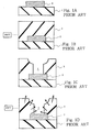
- FIG. 1A to 1H illustrate the prior art multiple-step high- temperature sputtering technology disclosed in the Japanese Patent Publication of Unexamined Application.
- Circuit components are fabricated on a silicon substrate (not shown), and are covered with a first inter-level insulating layer 1.
- a lower metal line 2 of aluminum is patterned on the lower inter-level insulating layer 1 as shown in figure 1A.
- Insulating material is deposited over the entire surface of the resultant structure by using a plasma-assisted chemical vapor deposition at 380 degrees in centigrade, and forms a second inter-level insulating layer 3 as shown in figure 1B.
- a photo- resist etching mask (not shown) is formed on the second inter-level insulating layer 3, and has an opening over the lower metal line 2. Using the photo- resist etching mask exposes a part of the second inter- level insulating layer 3 to an etchant, and the second inter- level insulating layer 3 is selectively etched away so as to form a via-hole 4 in the second inter- level insulating layer 3 as shown in figure 1C.
- an outgassing is carried out in high- temperature vacuum.
- the resultant structure is placed in vacuum, and is heated to 450 degrees in centigrade.
- the high-temperature vacuum ambience for the outgassing is higher in temperature than a sputtering temperature described hereinlater with reference to figure 1G.
- the second inter- level insulating layer 3 emits gas as indicated by arrows in figure 1D.
- titanium is deposited over the entire surface, and forms a titanium layer 5.
- the resultant structure is maintained in the vacuum chamber without breaking the vacuum, and aluminum is deposited over the entire surface in low- temperature ambience at a high sputtering rate.
- an aluminum layer 6 is deposited on the titanium layer 5 as shown in figure 1F.
- the aluminum layer 6 defines a secondary via-hole 7.
- aluminum is deposited over the entire surface of the resultant structure in a high- temperature ambience at a low sputtering rate without breaking the vacuum.
- the high- temperature low-rate sputtering results in a surface diffusion of aluminum.
- the aluminum fills the secondary via-hole 7, and swells into an aluminum layer 8.
- the aluminum layer 8 is merged into the aluminum layer 6, and the titanium reacts with the aluminum for forming a titanium- aluminum alloy layer 9 as shown in figure 1G.
- the titanium- aluminum layer 9 and the aluminum layer 8 are patterned into an upper metal line 10 by using the photo-lithography and an etching.
- the resultant wiring structure is shown in figure 1H.
- the high- temperature low- rate sputtering gives rise to the surface diffusion, and fills the miniature via-hole 7 with the aluminum. As a result, the step-coverage is surely improved.
- a problem is encountered in the prior art process in that hillocks and whiskers are grown from the lower metal line 2 due to the thermal stress. The hillocks and the whiskers are causative of a short- circuit between the aluminum lines.
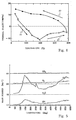
- the present inventor contemplated the problem. Although the lower metal line 2 of refractory metal such as tungsten or titanium nitride was free from the problem, the refractory metal and the refractory metal nitride were larger in resistivity than aluminum, and were not desirable for a high- speed integrated circuit. Then, the present inventor investigated the prior art process, and paid his attention to the outgassing step. The present inventor carried out the outgassing at different temperatures in the prior art process, and obtained plural groups of samples different in outgassing temperature. The present inventor observed the plural groups of samples to see how many lower metal lines 2 were damaged with the hillocks and the whiskers. The present inventor plotted the number of damaged samples in terms of the heating temperature as shown in figure 2.
- the present invention proposes to carry out an outgassing not higher than a deposition temperature of the inter-level insulating layer.
- a process for fabricating a semiconductor device comprising the steps of a) forming a lower metal line over a semiconductor substrate, b) covering the lower metal line with an inter- level insulating layer under the condition that the semiconductor substrate is heated to a first temperature at the maximum, c) forming a via- hole in the inter- level insulating layer, d) carrying out an outgassing under the condition that the semiconductor substrate is heated to a second temperature equal to or less than the first temperature so as to remove contaminants from the inter- level insulating layer and e) forming an upper metal line penetrating into the via- hole and formed of a conductive material selected from the group consisting of aluminum and aluminum alloys.
- FIGS 3A to 3H illustrate a process for fabricating a semiconductor device embodying the present invention. The process starts with preparation of a semiconductor substrate 20. Though not shown in figures 3A to 3H, circuit components such as field effect transistors of an integrated circuit are fabricated on the semiconductor substrate 20.
- Insulating material is deposited over the semiconductor substrate 20, and the circuit components are covered with a first inter-level insulating layer 21.
- Aluminum or aluminum alloy is deposited over the entire surface of the first inter-level insulating layer 21 by using a sputtering.
- the aluminum alloy is, by way of example, aluminum- copper alloy or aluminum- silicon- copper alloy.
- Photo- resist solution is spread over the entire surface of the aluminum/ aluminum alloy layer, and is baked so as to form a photo-resist layer.
- a pattern image for lower- metal lines is transferred to the photo-resist layer, and a latent image is produced in the photo- resist layer.
- the latent image is developed, and the photo-resist layer is shaped into a photo- resist etching mask (not shown).
- the aluminum/ aluminum alloy layer is selectively etched, and a lower- metal line 22 is left on the first inter- level insulating layer 21 as shown in figure 3A.
- the lower- metal line 22 is formed through the photo- lithography and the etching.
- insulating material in silicon oxide system is deposited over the entire surface of the resultant structure by using a plasma-assisted chemical vapor deposition, and forms a second inter-level insulating layer 23.
- the semiconductor substrate 20 is heated to a certain temperature TW.
- the certain temperature TW is 380 degrees in centigrade.
- the certain temperature TW ranges from 200 degrees to 600 degrees in centigrade.
- the certain temperature TW is usually fallen within the range between 400 degrees and 200 degrees in centigrade.
- the second inter-level insulating layer 23 may be chemically mechanically polished so as to create a smooth top surface.
- a photo-resist etching mask (not shown) is patterned on the second inter-level insulating layer 23 through the photo-lithography.
- the photo-resist etching mask exposes a part of the second inter-level insulating layer 23 over the lower metal line 22 to dry etchant and, thereafter, to wet etchant, and the dry etchant and the wet etchant form a via- hole 24 in the second inter-level insulating layer 23.
- the dry etchant anisotropically etches the part of the second inter- level insulating layer 23, and causes the via- hole 24 to have an aspect ratio not less than 1.
- the wet etchant isotropically etches an upper portion of the second inter-level insulating layer 23 around the via- hole 24, and rounds the periphery of the second inter- level insulating layer 23.
- the via-hole 24 is shaped into a funnel configuration as shown in figure 3C.
- the via-hole may be formed by using dry etchant only.
- the two- step sputtering has an outgassing step (see figure 3D), a cooling step, an improvement of wettability (see figure 3E), a low- temperature high- rate sputtering (see figure 3F) and a high- temperature low- rate sputtering (see figure 3G), and these steps are successively carried out in a sputtering chamber without breaking vacuum.
- the semiconductor substrate 20 is heated to 380 degrees in centigrade for the outgassing.
- Water H 2 O, the water component OH and other contaminants are vaporized, and are removed from the entire surface of the resultant structure as indicated by arrows in figure 3D.
- the substrate temperature in the outgassing is at least 200 degrees in centigrade. It is appropriate to carry out the outgassing at the substrate temperature lower than the certain temperature TW by zero to 400 degrees in centigrade. Thus, the substrate temperature in the outgassing is equal to or lower than the substrate temperature TW in the deposition of the second inter-level insulating layer 23.
- the semiconductor substrate 20 Upon completion of the outgassing, the semiconductor substrate 20 is cooled, and titanium is deposited over the entire surface of the resultant structure without any pre-heating.
- the titanium forms a titanium layer 25, and the titanium layer 25 conformably extends on the exposed surface of the second inter- level insulating layer 23 as shown in figure 3E.
- the titanium layer 25 improves the wettability for aluminum.
- the low- temperature high- rate sputtering is carried out.
- the semiconductor substrate 20 is not pre-heated or heated to a lower temperature not higher than 150 degrees in centigrade.
- Aluminum or aluminum alloy is deposited over the entire surface of the titanium layer 25, and forms an aluminum/ aluminum alloy layer 26.
- the aluminum alloy may be aluminum- copper alloy or aluminum- silicon- copper alloy.
- the low- temperature high- rate sputtering is completed before the aluminum/ aluminum alloy closes the via-hole as shown in figure 3F. For this reason, the aluminum/ aluminum alloy layer 26 defines a hollow space 27 in the via- hole 24.
- the low- temperature high- rate aluminum sputtering is followed by the high- temperature low- rate aluminum sputtering.
- the semiconductor substrate 20 is heated to 400 degrees to 500 degrees in centigrade, and the aluminum or the aluminum alloy is deposited over the resultant structure at 2000 ⁇ /min. or less.
- the aluminum/ aluminum alloy fills the hollow space 27, and swells into an aluminum/ aluminum alloy layer 28.
- the high temperature promotes the surface diffusion, and the surface diffusion improves the step coverage. While the aluminum/ aluminum alloy is being grown at the high temperature, the aluminum reacts with the titanium, and the titanium layer 25 is converted to an aluminum- titanium alloy layer 29.
- a photo- resist etching mask (not shown) is patterned on the aluminum/ aluminum alloy layer 28 through the photo-lithography, and the aluminum/ aluminum alloy layer 28 is selectively removed by using dry etchant.
- the aluminum- titanium layer 29 and the aluminum/ aluminum alloy layer 28 are patterned into an upper metal line 30 as shown in figure 3H.
- the present inventor investigated the thermal stress exerted on the lower metal line 22.
- the present inventor varied the temperature around the lower metal line 22, and determined the thermal stress exerted on the lower metal line 22.
- the thermal stress was plotted in figure 4. While the temperature was rising, the thermal stress was changed from the tensile stress to the compressive stress as indicated by arrow A1, and the compressive stress was maximized around 200 degrees in centigrade. After reaching the maximum compressive stress, the compressive stress was decreased together with the temperature as indicated by arrow A2. On the other hand, while the temperature was lowered, the compressive stress was changed to the tensile stress, and the tensile stress was increased inversely to the temperature as indicated by arrow A3.
- the lower metal line 22 When the lower metal line 22 was patterned, the tensile stress was exerted on the lower metal line 22. While the insulating material was being deposited for the second inter-level insulating layer 23, the lower metal line 22 was heated toward 380 degrees in centigrade, and the tensile stress was changed to the compressive stress (see arrow A1). However, the aluminum grains were grown in the high temperature ambience, and the compressive stress was decreased after 200 degrees in centigrade (see arrow A2). Upon completion of the deposition, the lower metal line was cooled as indicated by arrow A3, and the tensile stress was left on the lower metal line 22. However, the lower metal line 22 withstood the variation of thermal stress along the loop indicated by arrows A1, A2 and A3, and any hillock and any whisker were not observed.
- the outgassing was carried out at the substrate temperature not higher than the substrate temperature TW in the plasma-assisted chemical vapor deposition. This meant that the variation of thermal stress was equivalent to or milder than the variation of thermal stress in the deposition for the second inter-level insulating layer 23. For this reason, the lower metal line 22 withstood the thermal stress during the outgassing, and any hillock and any whisker did not take place. Thus, the lower- metal lines 22 were free from a short- circuit.
- the present inventor evaluated the substrate temperature during the outgassing.
- the present inventor carried out the outgassing at different temperatures, and measured variation of the contaminant such as CO 2 , N 2 , H 2 O and OH.
- the contaminants CO 2 , N 2 , H 2 O and OH were plotted in terms of the outgassing temperature in figure 5.
- the contaminant OH was decomposed from water H 2 O at the measurement, and both of the mass numbers 17 and 18 were representative of water.
- the residual contaminants were sufficiently reduced around 380 degrees in centigrade, and the outgassing temperature equal to the deposition temperature TW was acceptable for the process.
- the present inventor investigated the high- temperature low- rate sputtering.
- the high- temperature low- rate sputtering was carried out at the substrate temperature ranging between 400 degrees to 500 degrees in centigrade.
- the present inventor deposited the aluminum at 490 degrees in centigrade at a low deposition rate after the outgassing at 380 degrees in centigrade, and checked the samples to see whether or not a hillock or a whisker took plate in the lower metal lines 22.
- the present inventor confirmed that the lower metal lines 22 were never damaged.
- the aluminum layer 28 was formed by using the high- temperature low- rate sputtering, the high substrate temperature did not result in any hillock and any whisker. This phenomenon was derived from the constraint on the lower metal line 22.
- the outgassing had been carried out before the titanium layer 25 was deposited, and the lower metal line 22 was without any constraint.
- the aluminum/ aluminum alloy was deposited through the high- temperature low- rate sputtering after the formation of the titanium/ aluminum layers 25/ 26.
- the titanium/ aluminum layers 25/ 26 served as the constraint, and prevented the lower metal line 2 from a hillock and a whisker. Thus, only the outgassing had the influence on the lower metal line 22.
- the outgassing is carried out at the substrate temperature not higher than the substrate temperature for the deposition of the second inter-level insulating layer 23, and the lower metal line 22 withstands the thermal stress during the outgassing.
- the process according to the present invention improves the step coverage without sacrifice of the reliability of lower metal lines 22.
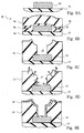
- Figures 6A to 6H illustrate another process for fabricating a semiconductor device embodying the present invention.
- the process also starts with preparation of a semiconductor substrate (not shown).
- Field effect transistors (not shown) are, by way of example, fabricated on the major surface portion of the semiconductor substrate.
- the field effect transistors are covered with a first inter-level insulating layer 31.
- Conductive material of aluminum or aluminum alloy is deposited over the entire surface of the first inter-level insulating layer 31, and forms an aluminum/ aluminum alloy layer.
- the aluminum alloy may be aluminum- copper alloy or aluminum- silicon- copper alloy.
- a photo-resist etching mask (not shown) is patterned on the aluminum/ aluminum alloy layer through the photo-lithography, and the aluminum/ aluminum alloy layer is selectively etched by using the photo-resist etching mask.
- the aluminum/ aluminum alloy layer is patterned into lower metal lines 32, one of which is shown in figure 6A.
- the lower metal lines 32 are covered with a second inter-level insulating layer 33 as follows.
- Silicon oxide is deposited over the entire surface by using a plasma-assisted chemical vapor deposition at 450 degrees in centigrade.
- the silicon oxide forms a silicon oxide layer 34, which conformably extends over the lower metal lines 32.
- the silicon oxide layer 34 prevents a silica layer 35 from cracking, and, accordingly, serves as a linear layer.
- Silica solution is spread over the silicon oxide layer 34, and forms the silica layer 35.
- the silica layer 35 also conformably extends over the silicon oxide layer 34, and is subjected to a dry etching without any etching mask.
- the silica layer 35 is etched back, and is left on the silicon oxide layer 34 between the lower metal lines 32.
- the etch-back step may be deleted from the process.
- Silicon oxide is deposited over the entire surface of the resultant structure by using the plasma-assisted chemical vapor deposition, again, and forms a silicon oxide layer 36.
- the silicon oxide layer 36 serves as a cap layer.
- the resultant structure is annealed at 450 degrees in centigrade, and the silica layer 35 is baked.
- the silicon oxide layers 34/ 36 and the silica layer 35 as a whole constitute the second inter-level insulating layer 33.
- the resultant structure is shown in figure 6B.
- a photo- resist etching mask (not shown) is patterned on the second inter-level insulating layer 33 by using the photo- lithography, and a via- hole 37 is formed in the second inter- level insulating layer 33 through the dry etching followed by the wet etching as shown in figure 6C.
- the via- hole 37 may be formed through the dry etching only.
- an upper metal line 38 is formed by using a multiple- step sputtering technique.
- the upper metal line 38 is formed of aluminum or aluminum alloy.
- the aluminum alloy is, by way of example, aluminum- copper alloy or aluminum- silicon- copper alloy.
- the resultant structure is placed in an air- tight chamber, and vacuum is developed in the air- tight chamber.
- an outgassing is carried out at 450 degrees in centigrade, which is equal to the deposition temperature of the silicon oxide layers 34/ 36 and the annealing temperature.
- the silica layer 35 contains much water. The outgassing temperature is high enough to remove the water and the contaminants as indicated by arrows in figure 6D.
- Titanium is conformably deposited over the entire surface of the resultant structure without any preheating by using the sputtering, and forms a titanium layer 39 as shown in figure 6E.
- the titanium layer 39 enhances the wettability for the aluminum/ aluminum alloy.
- the aluminum or the aluminum alloy is deposited over the titanium layer 39 at a low temperature and a high deposition rate.
- the vacuum is maintained in the air- tight chamber.
- the aluminum/ aluminum forms an aluminum/ aluminum alloy layer 40, which conformably extends on the titanium layer 39 as shown in figure 6F.
- the aluminum or the aluminum alloy is deposited over the aluminum/ aluminum alloy layer 40 at a high temperature and a low deposition rate without breaking the vacuum.
- the high- temperature ambience enhances the surface diffusion of aluminum/ aluminum alloy.
- the aluminum/ aluminum alloy fills the hollow space defined by the aluminum/ aluminum alloy layer 40 in the via- hole 37, and swells into an aluminum/ aluminum alloy layer 41 as shown in figure 6G. While the aluminum/ aluminum alloy is being deposited, the titanium reacts with the aluminum, and the titanium layer 39 is converted to a titanium- aluminum layer 42.
- a photo- resist etching mask (not shown) is patterned on the aluminum/ aluminum alloy layer 41, and the aluminum/ aluminum alloy layer 41 and the titanium- aluminum alloy layer 42 are selectively etched away by using a dry etching. Then, the upper metal line 38 is left on the second inter-level insulating layer 33 as shown in figure 6H.
- the outgassing is carried out at the temperature equal to the maximum temperature in the formation of second inter-level insulating layer, and any hillock, whisker and any void do not take place in the lower metal line 32.
- the silica layer 35 is moisture absorbent, the water and water component are eliminated from the silica layer through the outgassing, and the manufacturer can use the silica layer 35 as the smoothening technique.
- the outgassing is carried out at the certain temperature equal to or less than the maximum temperature in the inter- level insulating layer over the lower metal lines, and the outgassing according to the present invention does not damage the lower metal lines during the deposition of the aluminum/ aluminum alloy at the high temperature.
- the process according to the present invention enhances the reliability of the lower metal lines without a void in the via- holes.
- the multiple step sputtering technique may be replaced with an aluminum reflow technique, a high- temperature high- pressure sputtering or a high- temperature sputtering for the deposition of the aluminum/ aluminum alloy.
- the second inter- level insulating layer 33 may be smoothened by using a chemical mechanical polishing instead of the silica layer 35.
Landscapes
- Internal Circuitry In Semiconductor Integrated Circuit Devices (AREA)
- Formation Of Insulating Films (AREA)
Applications Claiming Priority (2)
| Application Number | Priority Date | Filing Date | Title |
|---|---|---|---|
| JP33780498A JP3329290B2 (ja) | 1998-11-27 | 1998-11-27 | 半導体装置の製造方法 |
| JP33780498 | 1998-11-27 |
Publications (2)
| Publication Number | Publication Date |
|---|---|
| EP1006571A2 true EP1006571A2 (fr) | 2000-06-07 |
| EP1006571A3 EP1006571A3 (fr) | 2002-07-17 |
Family
ID=18312133
Family Applications (1)
| Application Number | Title | Priority Date | Filing Date |
|---|---|---|---|
| EP99123516A Ceased EP1006571A3 (fr) | 1998-11-27 | 1999-11-25 | Procédé d'un dispositif semiconducteur avec une meilleure couverture en gradins de contacts sans sacrifier la fiabilité des linéaires d'aluminium |
Country Status (6)
| Country | Link |
|---|---|
| US (1) | US6444571B1 (fr) |
| EP (1) | EP1006571A3 (fr) |
| JP (1) | JP3329290B2 (fr) |
| KR (1) | KR100374981B1 (fr) |
| CN (1) | CN1124648C (fr) |
| TW (1) | TW444245B (fr) |
Cited By (1)
| Publication number | Priority date | Publication date | Assignee | Title |
|---|---|---|---|---|
| WO2019050630A1 (fr) * | 2017-09-11 | 2019-03-14 | General Electric Company | Système de pulvérisation et procédé de formation d'une couche métallique sur un dispositif à semi-conducteur |
Families Citing this family (6)
| Publication number | Priority date | Publication date | Assignee | Title |
|---|---|---|---|---|
| JP2002118167A (ja) * | 2000-10-06 | 2002-04-19 | Nec Corp | 半導体装置の製造方法 |
| US6794282B2 (en) | 2002-11-27 | 2004-09-21 | Infineon Technologies Ag | Three layer aluminum deposition process for high aspect ratio CL contacts |
| US7351656B2 (en) * | 2005-01-21 | 2008-04-01 | Kabushiki Kaihsa Toshiba | Semiconductor device having oxidized metal film and manufacture method of the same |
| CN102024747B (zh) * | 2009-09-11 | 2015-02-11 | 中芯国际集成电路制造(上海)有限公司 | 功率器件的铝插塞制作方法 |
| CN103390542A (zh) * | 2013-07-25 | 2013-11-13 | 上海宏力半导体制造有限公司 | Mim电容器的形成方法 |
| CN111128869A (zh) * | 2019-12-26 | 2020-05-08 | 华虹半导体(无锡)有限公司 | 优化热铝填孔能力的制备方法 |
Family Cites Families (10)
| Publication number | Priority date | Publication date | Assignee | Title |
|---|---|---|---|---|
| JPH0810693B2 (ja) | 1987-09-17 | 1996-01-31 | 東京エレクトロン株式会社 | 半導体装置の製造方法 |
| JPH01258444A (ja) * | 1988-04-08 | 1989-10-16 | Fujitsu Ltd | ドライ前処理装置 |
| CA2017720C (fr) * | 1990-05-29 | 1999-01-19 | Luc Ouellet | Verre centrifuge comprenant une couche de finition protectrice resistante a l'humidite. |
| CA2032763C (fr) * | 1990-12-20 | 2001-08-21 | Mitel Corporation | Prevention de la contamination du circuit de transit par desorption induite obtenue par decharge luminescente |
| JP2928409B2 (ja) | 1991-08-19 | 1999-08-03 | 松下電子工業株式会社 | 半導体装置の製造方法 |
| JPH0555225A (ja) | 1991-08-26 | 1993-03-05 | Sony Corp | 半導体装置の製造方法 |
| US5643407A (en) * | 1994-09-30 | 1997-07-01 | Taiwan Semiconductor Manufacturing Company, Ltd. | Solving the poison via problem by adding N2 plasma treatment after via etching |
| JPH0964037A (ja) | 1995-08-23 | 1997-03-07 | Mitsubishi Electric Corp | 半導体装置の製造方法 |
| US5789315A (en) * | 1996-07-17 | 1998-08-04 | Advanced Micro Devices, Inc. | Eliminating metal extrusions by controlling the liner deposition temperature |
| JPH10233444A (ja) | 1997-02-19 | 1998-09-02 | Mitsubishi Electric Corp | 半導体装置の製造方法 |
-
1998
- 1998-11-27 JP JP33780498A patent/JP3329290B2/ja not_active Expired - Fee Related
-
1999
- 1999-11-24 US US09/449,236 patent/US6444571B1/en not_active Expired - Fee Related
- 1999-11-25 TW TW088120747A patent/TW444245B/zh not_active IP Right Cessation
- 1999-11-25 EP EP99123516A patent/EP1006571A3/fr not_active Ceased
- 1999-11-26 CN CN99125090A patent/CN1124648C/zh not_active Expired - Fee Related
- 1999-11-26 KR KR10-1999-0052914A patent/KR100374981B1/ko not_active Expired - Fee Related
Cited By (2)
| Publication number | Priority date | Publication date | Assignee | Title |
|---|---|---|---|---|
| WO2019050630A1 (fr) * | 2017-09-11 | 2019-03-14 | General Electric Company | Système de pulvérisation et procédé de formation d'une couche métallique sur un dispositif à semi-conducteur |
| US10354871B2 (en) | 2017-09-11 | 2019-07-16 | General Electric Company | Sputtering system and method for forming a metal layer on a semiconductor device |
Also Published As
| Publication number | Publication date |
|---|---|
| KR100374981B1 (ko) | 2003-03-29 |
| KR20000035720A (ko) | 2000-06-26 |
| US6444571B1 (en) | 2002-09-03 |
| CN1124648C (zh) | 2003-10-15 |
| JP3329290B2 (ja) | 2002-09-30 |
| CN1255747A (zh) | 2000-06-07 |
| EP1006571A3 (fr) | 2002-07-17 |
| TW444245B (en) | 2001-07-01 |
| JP2000164708A (ja) | 2000-06-16 |
Similar Documents
| Publication | Publication Date | Title |
|---|---|---|
| JP3729882B2 (ja) | アルミニウムコンタクト形成方法 | |
| US5604156A (en) | Wire forming method for semiconductor device | |
| EP0499433B1 (fr) | Dispositif semi-conducteur ayant un cablage à fonctionnement amélioré, et procédé pour sa fabrication | |
| US5356836A (en) | Aluminum plug process | |
| EP0571108B1 (fr) | Structure d'un trou de contact pour un dispositif semi-conducteur et son procédé de fabrication | |
| US7714440B2 (en) | Metal interconnection structure of a semiconductor device having low resistance and method of fabricating the same | |
| US6444571B1 (en) | Process for fabricating a semiconductor device with improved step coverage and reliability of a lower aluminum line | |
| JPH0766942B2 (ja) | 多層相互接続導体パターン製造方法 | |
| US6566211B2 (en) | Surface modified interconnects | |
| US5418187A (en) | Method for extending electrically conductive layer into electrically insulating layer | |
| US5521116A (en) | Sidewall formation process for a top lead fuse | |
| US6080657A (en) | Method of reducing AlCu hillocks | |
| US6355983B2 (en) | Surface modified interconnects | |
| US6812113B1 (en) | Process for achieving intermetallic and/or intrametallic air isolation in an integrated circuit, and integrated circuit obtained | |
| JP2537467B2 (ja) | 半導体装置の製造方法 | |
| JP2004031911A (ja) | 金属突き出しのないビアを形成する方法 | |
| US6261949B1 (en) | Method for manufacturing semiconductor device | |
| US6680537B1 (en) | Semiconductor device having a dual damascene interconnect structure and method for manufacturing same | |
| US5994213A (en) | Aluminum plug process | |
| JPH08274101A (ja) | 半導体装置の配線構造の形成方法 | |
| JPH08139190A (ja) | 半導体装置の製造方法 | |
| JP3549425B2 (ja) | 半導体装置及びその製造方法 | |
| JPH07135250A (ja) | 半導体装置の製造方法 | |
| JP2000216239A (ja) | 銅内部結線の形成方法 | |
| KR100228278B1 (ko) | 반도체 장치의 제조 방법 |
Legal Events
| Date | Code | Title | Description |
|---|---|---|---|
| PUAI | Public reference made under article 153(3) epc to a published international application that has entered the european phase |
Free format text: ORIGINAL CODE: 0009012 |
|
| AK | Designated contracting states |
Kind code of ref document: A2 Designated state(s): AT BE CH CY DE DK ES FI FR GB GR IE IT LI LU MC NL PT SE |
|
| AX | Request for extension of the european patent |
Free format text: AL;LT;LV;MK;RO;SI |
|
| PUAL | Search report despatched |
Free format text: ORIGINAL CODE: 0009013 |
|
| AK | Designated contracting states |
Kind code of ref document: A3 Designated state(s): AT BE CH CY DE DK ES FI FR GB GR IE IT LI LU MC NL PT SE |
|
| AX | Request for extension of the european patent |
Free format text: AL;LT;LV;MK;RO;SI |
|
| 17P | Request for examination filed |
Effective date: 20020723 |
|
| AKX | Designation fees paid |
Designated state(s): DE GB |
|
| RAP1 | Party data changed (applicant data changed or rights of an application transferred) |
Owner name: NEC ELECTRONICS CORPORATION |
|
| APBN | Date of receipt of notice of appeal recorded |
Free format text: ORIGINAL CODE: EPIDOSNNOA2E |
|
| APBR | Date of receipt of statement of grounds of appeal recorded |
Free format text: ORIGINAL CODE: EPIDOSNNOA3E |
|
| APAF | Appeal reference modified |
Free format text: ORIGINAL CODE: EPIDOSCREFNE |
|
| RAP1 | Party data changed (applicant data changed or rights of an application transferred) |
Owner name: RENESAS ELECTRONICS CORPORATION |
|
| APBT | Appeal procedure closed |
Free format text: ORIGINAL CODE: EPIDOSNNOA9E |
|
| STAA | Information on the status of an ep patent application or granted ep patent |
Free format text: STATUS: THE APPLICATION HAS BEEN REFUSED |
|
| 18R | Application refused |
Effective date: 20101012 |