EP1006578A2 - Module semiconducteur de puissance - Google Patents
Module semiconducteur de puissance Download PDFInfo
- Publication number
- EP1006578A2 EP1006578A2 EP99123702A EP99123702A EP1006578A2 EP 1006578 A2 EP1006578 A2 EP 1006578A2 EP 99123702 A EP99123702 A EP 99123702A EP 99123702 A EP99123702 A EP 99123702A EP 1006578 A2 EP1006578 A2 EP 1006578A2
- Authority
- EP
- European Patent Office
- Prior art keywords
- semiconductor
- igbt
- devices
- module
- semiconductor devices
- Prior art date
- Legal status (The legal status is an assumption and is not a legal conclusion. Google has not performed a legal analysis and makes no representation as to the accuracy of the status listed.)
- Granted
Links
Images





Classifications
-
- H—ELECTRICITY
- H10—SEMICONDUCTOR DEVICES; ELECTRIC SOLID-STATE DEVICES NOT OTHERWISE PROVIDED FOR
- H10W—GENERIC PACKAGES, INTERCONNECTIONS, CONNECTORS OR OTHER CONSTRUCTIONAL DETAILS OF DEVICES COVERED BY CLASS H10
- H10W90/00—Package configurations
-
- H—ELECTRICITY
- H10—SEMICONDUCTOR DEVICES; ELECTRIC SOLID-STATE DEVICES NOT OTHERWISE PROVIDED FOR
- H10W—GENERIC PACKAGES, INTERCONNECTIONS, CONNECTORS OR OTHER CONSTRUCTIONAL DETAILS OF DEVICES COVERED BY CLASS H10
- H10W72/00—Interconnections or connectors in packages
- H10W72/30—Die-attach connectors
-
- H—ELECTRICITY
- H10—SEMICONDUCTOR DEVICES; ELECTRIC SOLID-STATE DEVICES NOT OTHERWISE PROVIDED FOR
- H10W—GENERIC PACKAGES, INTERCONNECTIONS, CONNECTORS OR OTHER CONSTRUCTIONAL DETAILS OF DEVICES COVERED BY CLASS H10
- H10W72/00—Interconnections or connectors in packages
- H10W72/60—Strap connectors, e.g. thick copper clips for grounding of power devices
-
- H—ELECTRICITY
- H10—SEMICONDUCTOR DEVICES; ELECTRIC SOLID-STATE DEVICES NOT OTHERWISE PROVIDED FOR
- H10W—GENERIC PACKAGES, INTERCONNECTIONS, CONNECTORS OR OTHER CONSTRUCTIONAL DETAILS OF DEVICES COVERED BY CLASS H10
- H10W72/00—Interconnections or connectors in packages
- H10W72/071—Connecting or disconnecting
- H10W72/073—Connecting or disconnecting of die-attach connectors
- H10W72/07331—Connecting techniques
- H10W72/07336—Soldering or alloying
-
- H—ELECTRICITY
- H10—SEMICONDUCTOR DEVICES; ELECTRIC SOLID-STATE DEVICES NOT OTHERWISE PROVIDED FOR
- H10W—GENERIC PACKAGES, INTERCONNECTIONS, CONNECTORS OR OTHER CONSTRUCTIONAL DETAILS OF DEVICES COVERED BY CLASS H10
- H10W72/00—Interconnections or connectors in packages
- H10W72/071—Connecting or disconnecting
- H10W72/075—Connecting or disconnecting of bond wires
- H10W72/07551—Connecting or disconnecting of bond wires characterised by changes in properties of the bond wires during the connecting
- H10W72/07553—Connecting or disconnecting of bond wires characterised by changes in properties of the bond wires during the connecting changes in shapes
-
- H—ELECTRICITY
- H10—SEMICONDUCTOR DEVICES; ELECTRIC SOLID-STATE DEVICES NOT OTHERWISE PROVIDED FOR
- H10W—GENERIC PACKAGES, INTERCONNECTIONS, CONNECTORS OR OTHER CONSTRUCTIONAL DETAILS OF DEVICES COVERED BY CLASS H10
- H10W72/00—Interconnections or connectors in packages
- H10W72/071—Connecting or disconnecting
- H10W72/076—Connecting or disconnecting of strap connectors
- H10W72/07631—Techniques
- H10W72/07637—Techniques using a polymer adhesive, e.g. an adhesive based on silicone or epoxy
-
- H—ELECTRICITY
- H10—SEMICONDUCTOR DEVICES; ELECTRIC SOLID-STATE DEVICES NOT OTHERWISE PROVIDED FOR
- H10W—GENERIC PACKAGES, INTERCONNECTIONS, CONNECTORS OR OTHER CONSTRUCTIONAL DETAILS OF DEVICES COVERED BY CLASS H10
- H10W72/00—Interconnections or connectors in packages
- H10W72/50—Bond wires
- H10W72/531—Shapes of wire connectors
-
- H—ELECTRICITY
- H10—SEMICONDUCTOR DEVICES; ELECTRIC SOLID-STATE DEVICES NOT OTHERWISE PROVIDED FOR
- H10W—GENERIC PACKAGES, INTERCONNECTIONS, CONNECTORS OR OTHER CONSTRUCTIONAL DETAILS OF DEVICES COVERED BY CLASS H10
- H10W72/00—Interconnections or connectors in packages
- H10W72/50—Bond wires
- H10W72/531—Shapes of wire connectors
- H10W72/5363—Shapes of wire connectors the connected ends being wedge-shaped
-
- H—ELECTRICITY
- H10—SEMICONDUCTOR DEVICES; ELECTRIC SOLID-STATE DEVICES NOT OTHERWISE PROVIDED FOR
- H10W—GENERIC PACKAGES, INTERCONNECTIONS, CONNECTORS OR OTHER CONSTRUCTIONAL DETAILS OF DEVICES COVERED BY CLASS H10
- H10W72/00—Interconnections or connectors in packages
- H10W72/50—Bond wires
- H10W72/541—Dispositions of bond wires
- H10W72/5445—Dispositions of bond wires being orthogonal to a side surface of the chip, e.g. parallel arrangements
-
- H—ELECTRICITY
- H10—SEMICONDUCTOR DEVICES; ELECTRIC SOLID-STATE DEVICES NOT OTHERWISE PROVIDED FOR
- H10W—GENERIC PACKAGES, INTERCONNECTIONS, CONNECTORS OR OTHER CONSTRUCTIONAL DETAILS OF DEVICES COVERED BY CLASS H10
- H10W72/00—Interconnections or connectors in packages
- H10W72/50—Bond wires
- H10W72/541—Dispositions of bond wires
- H10W72/547—Dispositions of multiple bond wires
- H10W72/5475—Dispositions of multiple bond wires multiple bond wires connected to common bond pads at both ends of the wires
-
- H—ELECTRICITY
- H10—SEMICONDUCTOR DEVICES; ELECTRIC SOLID-STATE DEVICES NOT OTHERWISE PROVIDED FOR
- H10W—GENERIC PACKAGES, INTERCONNECTIONS, CONNECTORS OR OTHER CONSTRUCTIONAL DETAILS OF DEVICES COVERED BY CLASS H10
- H10W72/00—Interconnections or connectors in packages
- H10W72/50—Bond wires
- H10W72/551—Materials of bond wires
- H10W72/552—Materials of bond wires comprising metals or metalloids, e.g. silver
- H10W72/5524—Materials of bond wires comprising metals or metalloids, e.g. silver comprising aluminium [Al]
-
- H—ELECTRICITY
- H10—SEMICONDUCTOR DEVICES; ELECTRIC SOLID-STATE DEVICES NOT OTHERWISE PROVIDED FOR
- H10W—GENERIC PACKAGES, INTERCONNECTIONS, CONNECTORS OR OTHER CONSTRUCTIONAL DETAILS OF DEVICES COVERED BY CLASS H10
- H10W72/00—Interconnections or connectors in packages
- H10W72/60—Strap connectors, e.g. thick copper clips for grounding of power devices
- H10W72/651—Materials of strap connectors
- H10W72/652—Materials of strap connectors comprising metals or metalloids, e.g. silver
-
- H—ELECTRICITY
- H10—SEMICONDUCTOR DEVICES; ELECTRIC SOLID-STATE DEVICES NOT OTHERWISE PROVIDED FOR
- H10W—GENERIC PACKAGES, INTERCONNECTIONS, CONNECTORS OR OTHER CONSTRUCTIONAL DETAILS OF DEVICES COVERED BY CLASS H10
- H10W72/00—Interconnections or connectors in packages
- H10W72/60—Strap connectors, e.g. thick copper clips for grounding of power devices
- H10W72/651—Materials of strap connectors
- H10W72/655—Materials of strap connectors of outermost layers of multilayered strap connectors, e.g. material of a coating
-
- H—ELECTRICITY
- H10—SEMICONDUCTOR DEVICES; ELECTRIC SOLID-STATE DEVICES NOT OTHERWISE PROVIDED FOR
- H10W—GENERIC PACKAGES, INTERCONNECTIONS, CONNECTORS OR OTHER CONSTRUCTIONAL DETAILS OF DEVICES COVERED BY CLASS H10
- H10W72/00—Interconnections or connectors in packages
- H10W72/851—Dispositions of multiple connectors or interconnections
- H10W72/853—On the same surface
- H10W72/871—Bond wires and strap connectors
-
- H—ELECTRICITY
- H10—SEMICONDUCTOR DEVICES; ELECTRIC SOLID-STATE DEVICES NOT OTHERWISE PROVIDED FOR
- H10W—GENERIC PACKAGES, INTERCONNECTIONS, CONNECTORS OR OTHER CONSTRUCTIONAL DETAILS OF DEVICES COVERED BY CLASS H10
- H10W72/00—Interconnections or connectors in packages
- H10W72/851—Dispositions of multiple connectors or interconnections
- H10W72/874—On different surfaces
- H10W72/884—Die-attach connectors and bond wires
-
- H—ELECTRICITY
- H10—SEMICONDUCTOR DEVICES; ELECTRIC SOLID-STATE DEVICES NOT OTHERWISE PROVIDED FOR
- H10W—GENERIC PACKAGES, INTERCONNECTIONS, CONNECTORS OR OTHER CONSTRUCTIONAL DETAILS OF DEVICES COVERED BY CLASS H10
- H10W72/00—Interconnections or connectors in packages
- H10W72/90—Bond pads, in general
- H10W72/921—Structures or relative sizes of bond pads
- H10W72/926—Multiple bond pads having different sizes
-
- H—ELECTRICITY
- H10—SEMICONDUCTOR DEVICES; ELECTRIC SOLID-STATE DEVICES NOT OTHERWISE PROVIDED FOR
- H10W—GENERIC PACKAGES, INTERCONNECTIONS, CONNECTORS OR OTHER CONSTRUCTIONAL DETAILS OF DEVICES COVERED BY CLASS H10
- H10W74/00—Encapsulations, e.g. protective coatings
-
- H—ELECTRICITY
- H10—SEMICONDUCTOR DEVICES; ELECTRIC SOLID-STATE DEVICES NOT OTHERWISE PROVIDED FOR
- H10W—GENERIC PACKAGES, INTERCONNECTIONS, CONNECTORS OR OTHER CONSTRUCTIONAL DETAILS OF DEVICES COVERED BY CLASS H10
- H10W90/00—Package configurations
- H10W90/701—Package configurations characterised by the relative positions of pads or connectors relative to package parts
- H10W90/751—Package configurations characterised by the relative positions of pads or connectors relative to package parts of bond wires
- H10W90/753—Package configurations characterised by the relative positions of pads or connectors relative to package parts of bond wires between laterally-adjacent chips
-
- H—ELECTRICITY
- H10—SEMICONDUCTOR DEVICES; ELECTRIC SOLID-STATE DEVICES NOT OTHERWISE PROVIDED FOR
- H10W—GENERIC PACKAGES, INTERCONNECTIONS, CONNECTORS OR OTHER CONSTRUCTIONAL DETAILS OF DEVICES COVERED BY CLASS H10
- H10W90/00—Package configurations
- H10W90/701—Package configurations characterised by the relative positions of pads or connectors relative to package parts
- H10W90/751—Package configurations characterised by the relative positions of pads or connectors relative to package parts of bond wires
- H10W90/754—Package configurations characterised by the relative positions of pads or connectors relative to package parts of bond wires between a chip and a stacked insulating package substrate, interposer or RDL
Definitions
- the present invention relates to semiconductor modules used in power conversion devices such as inverters and converters, and particularly to the arrangement of semiconductor devices in the module.
- the semiconductor modules used in power conversion devices include MOSFET modules containing a plurality of MOSFET (Metal Oxide Semiconductor Field Effect Transistor) devices, diode modules containing a plurality of diode devices, and IGBT modules containing a plurality of IGBT (Insulated Gate Bipolar Transistor) devices and diode devices, for example.
- MOSFET Metal Oxide Semiconductor Field Effect Transistor
- diode modules containing a plurality of diode devices diode modules containing a plurality of diode devices
- IGBT modules containing a plurality of IGBT (Insulated Gate Bipolar Transistor) devices and diode devices for example.
- IGBT modules containing a plurality of semiconductor devices, IGBT devices and diode devices, connected in parallel will be described herein as an example of the semiconductor module.
- the conventional IGBT modules include that described in "A Novel Low-Cost and High-Reliability IGBT Module for General Use," written by E.Tamba, M.Sasaki, S.Sekine, Y.Sonobe, K.Suzuki, K.Yamada, R.Saito, T.Terasaki, O.Suzuki, T.Shigemura et al. European Conference on Power Electronics and Applications 1997, Trondheim, for example.
- Fig.8 is a plane view mainly showing the semiconductor device area in this conventional IGBT module
- Fig.9 is a sectional view mainly showing an area including an IGBT device and a diode device in the module.
- the conventional semiconductor module includes a radiation board 1 made of metal, e.g. copper, for cooling the semiconductor devices, insulating substrates 2 made of aluminum nitride or the like and bonded on the radiation board 1, electrode patterns 2a bonded on both sides of the insulating substrates 2, and IGBT devices 3 and diode devices 4 as semiconductor devices bonded on the metal patterns 2a on the insulating substrates 2.
- Each IGBT device 3 has an emitter electrode 5 and a gate electrode 6 formed on its one side and a collector electrode 7 formed on the entire surface on the other side, and each diode device 4 has an anode electrode 8 formed on its one side and a cathode electrode 9 formed on the entire surface on the other side thereof.
- Emitter relay substrates 10, collector relay substrates 11, and gate interconnection substrates 12 are bonded on the radiation board 1, and electrode patterns 10a, 11a and 12a are respectively bonded on both sides of the substrates.
- It also includes aluminum wires 13a, 13b, 13c as interconnections, a module emitter electrode 14, a module collector electrode 15, and module gate electrodes 16 as external terminals, a case 17 made of a resin material and fixed on the radiation board 1, and resin 18 sealing the inside of the case 17.
- the insulating substrates 2 are bonded with solder on the radiation board 1 and the IGBT devices 3 and the diode devices 4 are bonded side by side with solder on the electrode patterns 2a on the insulating substrates 2.
- Each emitter electrode 5 on the surface of the IGBT device 3 and the anode electrode 8 on the surface of the diode device 4 are connected through the aluminum wires 13a, which are further connected to the electrode pattern 10a on the emitter relay substrate 10.
- the electrode pattern 2a on the insulating substrate 2, to which the IGBT device 3 and the diode device 4 are bonded, is connected to the electrode pattern 11a on the collector relay substrate 11 through the aluminum wires 13b, so as to connect the collector electrode 7 on the back of the IGBT device 3, the cathode electrode 9 on the back of the diode device 4, and the electrode pattern 11a on the collector relay substrate 11.
- this semiconductor module contains four IGBT devices 3 and four diode devices 4, where the IGBT devices 3 and the diode devices 4 are connected in inverse parallel. That is to say, the devices are connected to form one module in such a manner that the emitter electrode 5 of the IGBT device 3 and the anode electrode 8 of the diode device 4 are at the same potential and the collector electrode 7 of the IGBT device 3 and the cathode electrode 9 of the diode device 4 are at the same potential.
- the module emitter electrode 14 as an external emitter terminal is connected to the electrode patterns 10a on the emitter relay substrates 10, and the module collector electrode 15 as an external collector terminal is connected to the electrode patterns 11a on the collector relay substrates 11.
- These external terminals 14 and 15 make connections to other semiconductor modules and the like (not shown) outside the case 17 to form a circuit like an inverter.
- the gate electrode 6 of each IGBT device 3 is connected to the electrode pattern 12a on the gate interconnection substrate 12 through the aluminum wire 13c to control the gate potential for turning on/off the IGBT device 3, and the electrode pattern 12a is further connected to the module gate electrode 16 serving as an external gate terminal.
- Fig.10 shows a circuit diagram of a three-phase inverter circuit as a typical example of a circuit to which the IGBT module is applied.
- Fig.10 shows IGBT modules 19 on the positive side, IGBT modules 20 on the negative side, a positive terminal 21 of DC voltage source, a negative terminal 22 of DC voltage source, a collector terminal 23 of the positive-side IGBT module 19 in the U phase, and an emitter terminal 24 of the negative-side IGBT module 20.
- the connection point 25 between the emitter terminal of the positive-side IGBT module 19 and the collector terminal of the negative-side IGBT module 20 is a U-phase output terminal.
- the power conversion devices like inverters using the semiconductor modules are used as motor driving power source in trains, for example, which are usually installed in limited space. Therefore size reduction is extremely important.
- the semiconductor devices in the IGBT module, or the IGBT device 3 and the diode device 4 are provided side by side in the lateral direction on the radiation board 1 with the insulating substrate 2 therebetween so that the heat generated in operation can be conducted to the radiation board 1 for cooling.
- the emitter electrode 5 and the anode electrode 8 formed on the surfaces of the devices 3 and 4 are connected by wire bonding through the aluminum wires 13a.
- the area reduction of the IGBT module in the plane direction (the direction in which the semiconductor devices 3 and 4 are arranged) is limited, which hinders effective size reduction of the IGBT module.
- a semiconductor module comprises: a first semiconductor device; a second semiconductor device; and a case for accommodating the first and second semiconductor devices, wherein the first and second semiconductor devices have their respective main electrodes, and the first and second semiconductor devices are stacked, with an element connecting conductor interposed between the main electrodes.
- the first and second semiconductor devices are stacked, with their respective main electrodes facing each other.
- the first and second semiconductor devices are the same kind of semiconductor devices.
- the main electrodes of the first and second semiconductor devices are main electrodes having the same function.
- the main electrodes of the first and second semiconductor devices are main electrodes having opposite functions.
- the first semiconductor device is an IGBT device
- the second semiconductor device is a diode device
- the semiconductor module further comprises a radiation board on which the IGBT device is provided, and the diode device is provided right above the IGBT device.
- the first and second semiconductor devices and the element connecting conductor are bonded together with a conductive resin.
- the semiconductor module further comprises a pressurizing mechanism for pressurizing the first and second semiconductor devices from outside in directions in which the main electrodes of the first and second semiconductor devices face each other, and the first and second semiconductor devices are joined together by pressure connection with the element connecting conductor interposed therebetween.
- the case comprises two conductive radiation boards, the first and second semiconductor devices stacked with the element connecting conductor interposed therebetween are provided between the two conductive radiation boards, and the pressurizing mechanism pressurizes the two conductive radiation boards in the facing directions.
- the first semiconductor device and the second semiconductor device are stacked and connected through an element connecting conductor and accommodated in a case. This reduces the area of the semiconductor module and effectively achieves size reduction.
- the first and second semiconductor devices are stacked with their respective main electrodes facing each other. This improves the cooling performance of the semiconductor module.
- the first and second semiconductor devices are the same kind of semiconductor devices. This reduces the area of the semiconductor module by half and achieves further size reduction.
- the respective main electrodes of the first and second semiconductor devices are main electrodes having the same function. Then the electric characteristics of the first semiconductor device and the second semiconductor device can be uniform and stable.
- the respective main electrodes of the first and second semiconductor devices are main electrodes having opposite functions. This effectively achieves the size reduction of the semiconductor module in which semiconductor devices of the same kind are connected in parallel.
- an IGBT device is provided on a radiation board and a diode device is provided right above the IGBT device. This provides a semiconductor module having excellent cooling performance.
- the first and second semiconductor devices and the element connecting conductor are bonded together by a conductive resin.
- the semiconductor devices can be bonded to the element connecting conductor reliably and easily, which facilitates the process of assembling the semiconductor module.
- the first and second semiconductor devices are joined together by pressure connection with the element connecting conductor interposed therebetween.
- the semiconductor devices can be easily joined to the element connecting conductor, which simplifies the process of manufacturing the semiconductor module.
- the case has two conductive radiation boards and first and second semiconductor devices stacked with the element connecting conductor interposed therebetween are provided between the two conductive radiation boards.
- the two conductive radiation boards are pressurized by the pressurizing mechanism in the facing directions. This allows easy and simple manufacture of an effectively downsized semiconductor module having excellent cooling performance.
- the present invention has been made to solve the problems above, and an object of the present invention is to provide a module structure which can effectively promote size reduction of a semiconductor module containing a plurality of semiconductor devices connected to realize large-power switching.
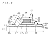
- Figs.1 and 2 show the structure of an IGBT module 100 according to the first preferred embodiment of the present invention, where Fig.1 is a plane view and Fig.2 is a partial sectional view.
- This IGBT module contains semiconductor devices in a case; the case is not shown in the diagrams for simplicity.
- the IGBT module 100 has a radiation board 26 made of metal, e.g. copper, for cooling the semiconductor devices, insulating substrates 27 made of aluminum nitride or the like and bonded on the radiation board 26, electrode patterns 27a bonded on both sides of the insulating substrates 27, IGBT devices 28 as first semiconductor devices bonded on the metal patterns 27a on the insulating substrates 27, and diode devices 29 as second semiconductor devices provided over the IGBT devices 28.
- a radiation board 26 made of metal, e.g. copper, for cooling the semiconductor devices
- insulating substrates 27 made of aluminum nitride or the like and bonded on the radiation board 26
- electrode patterns 27a bonded on both sides of the insulating substrates
- IGBT devices 28 as first semiconductor devices bonded on the metal patterns 27a on the insulating substrates
- diode devices 29 as second semiconductor devices provided over the IGBT devices 28.
- Each IGBT device 28 has an emitter electrode 30 and a gate electrode 31 formed on its one side and a collector electrode 32 formed on the entire surface on the other side, and each diode device 29 has an anode electrode 33 formed on its one side and a cathode electrode 34 formed on the entire surface on the other side.
- An element connecting conductor 35 made of metal, e.g. copper, is interposed between the IGBT device 28 and the diode device 29, and conductive resin 36 joins the IGBT device 28 and the diode device 29 to the element connecting conductor 35.
- Electrode patterns 37a, 38a, and 39a are bonded respectively on both sides of emitter relay substrates 37, collector relay substrates 38, and gate interconnection substrates 39 bonded on the radiation board 26. It also has aluminum wires 40, 41, and 42 as interconnections.
- each insulating substrate 27 is bonded on the radiation board 26 by solder and the surface of the IGBT device 28 on which the collector electrode 32 is formed is bonded by solder on the electrode pattern 27a on the insulating substrate 27.
- the emitter electrode 30 on the surface of the IGBT device 28 and the element connecting conductor 35, and the element connecting conductor 35 and the anode electrode 33 of the diode device 29, are joined together by the conductive resin 36.
- the emitter electrode 30 is connected to the electrode pattern 37a on the emitter relay substrate 37 through the aluminum wire 40.
- the upper surface of the diode device 29, the electrode pattern 27a on the insulating substrate 27 to which the IGBT device 28 is joined, and the electrode pattern 38a on the collector relay substrate 38 are connected through the aluminum wire 41.
- the collector electrode 32 on the back of the IGBT device 28, the cathode electrode 34 on the upper surface of the diode device 29, and the electrode pattern 38a on the collector relay substrate 38 are connected to each other.
- this semiconductor module has four IGBT devices 28 and four diode devices 29, where the devices 28 and 29 are stacked, with the emitter electrode 30 of the IGBT device 28 and the anode electrode 33 of the diode device 29 facing each other.
- the IGBT device 28 and the diode device 29 are connected in inverse parallel. That is to say, the devices are connected to form one module in such a manner that the emitter electrode 30 of the IGBT device 28 and the anode electrode 33 of the diode device 29 are at the same potential and the collector electrode 32 of the IGBT device 28 and the cathode electrode 34 of the diode device 29 are at the same potential.
- the gate electrode 31 of the IGBT device 28 is connected to the electrode pattern 39a on the gate interconnection substrate 39 through the aluminum wire 42 to control the gate potential for turning on/off the IGBT device 28.
- the module thus constructed further comprises a case (not shown) fixed on the radiation board 26 and the module is contained in this case and sealed with resin.
- the electrode patterns 37a, 38a, and 39a are connected to external module terminals (not shown).
- the area of the module can be reduced by the area approximately equal to the area of the diode device 29, since the diode device 29 is laid over the IGBT device 28, and this preferred embodiment can effectively achieve the size reduction.
- the emitter electrode 30 of the IGBT device 28 and the anode electrode 33 of the diode device 29 are joined to the element connecting conductor 35 with the conductive resin 36. That is, the IGBT device 28 and the diode device 29 are stacked and joined together through the element connecting conductor 35.
- the conductive resin 36 is made of epoxy resin with silver filler. It is applied to the surface between two members to be bonded and hardened at a temperature of about 150°C to keep the bonding strength at the bonded surface.
- the emitter electrode 30 of the IGBT device 28 and the anode electrode 33 of the diode device 29 were electrically connected by wire bonding through the aluminum wire 13a having small sectional area. Connecting them through the element connecting conductor 35 having large sectional area allows the heat generated by the diode device 29 in operation to conduct to the radiation board 26 through the element connecting conductor 35 and the IGBT device 28. Furthermore, in this preferred embodiment, the diode device 29 is laid right above the IGBT device 28, so that a short heat conducting path is formed from the diode device 29 to the radiation board 26 through the element connecting conductor 35 and the IGBT device 28, which reduces the thermal resistance and improves the performance of cooling the diode device 29.
- the IGBT device 28 usually generates a greater deal of heat than the diode device 29 when operating. Accordingly when the IGBT device 28 is provided on the radiation board 26 with the insulating substrate 27 interposed therebetween and the diode device 29 is laid further above it with the element connecting conductor 35 therebetween, the heat can be effectively conducted to the radiation board 26 to provide excellent cooling performance.
- the conductive resin 36 is not fluidic. Accordingly, when joining the emitter electrode 30 of the IGBT device 28 and the element connecting conductor 35, for example, the conductive resin 36 can be easily applied only to the emitter electrode 30 on the surface of the IGBT device 28. This allows the IGBT device 28 and the element connecting conductor 35 to be joined together without causing short circuit with the gate electrode 31 formed on the same surface. In this way, it is possible to reliably and easily bond the desired electrodes formed on the surfaces of the IGBT device 28 and the diode device 29 to the element connecting conductor 35, which facilitates the assembly process of the module.
- the element connecting conductor 35 is made of a material having high heat conductivity, and other metals like molybdenum can be used as well as copper.
- molybdenum can reduce distortion due to thermal stress because its linear expansion coefficient is close to that of silicon used to form the IGBT device 28 and the diode device 29.
- the IGBT device 28 and the diode device 29 may be connected to the element connecting conductor 35 with a conductive bond material other than the conductive resin 36.
- a conductive bond material other than the conductive resin 36.
- solder is used to join the emitter electrode 30 of the IGBT device 28 and the element connecting conductor 35, the gate electrode 31 surface is covered by a mask material and the solder is applied only to the emitter electrode 30.
- FIG.3 is a plane view showing the structure of an IGBT module 200 of the second preferred embodiment.
- One diode device 29 is provided for each IGBT device 28 in the examples of modules shown in the first preferred embodiment and the background art.
- the IGBT devices 28 may require a different number of diode devices 29 depending on the current capacity of the diode device 29, and only a single diode device 29 may be required for two IGBT devices 28.
- This preferred embodiment shows an example in which one diode device 29 is provided for every two IGBT devices 28.
- the module contains four IGBT devices 28a, 28b, 28c, and 28d as first semiconductor devices and two diode devices 29a and 29b as second semiconductor devices.
- the surfaces of the two IGBT devices 28a and 28b (or 28c and 28d) on which the collector electrodes 32 are formed are provided on the radiation board 26 with the insulating substrates 27 interposed therebetween.
- An element connecting conductor 35a (or 35b) is bonded on their emitter electrode 30 surfaces and the anode electrode 33 of the diode device 29a (or 29b) is bonded on the upper surface of the element connecting conductor 35a (or 35b).
- the entire structure is accommodated in a case not shown.
- the IGBT devices 28a and 28b (or 28c and 28d) and the diode device 29a (or 29b) are stacked and joined together in the vertical direction with the element connecting conductor 35a (or 35b) interposed therebetween.
- the emitter electrode 30 is connected to the electrode pattern 37a on the emitter relay substrate 37 through the aluminum wires 40.
- the upper surface of the diode device 29a (or 29b) is connected to the electrode patterns 27a on the insulating substrates 27 to which the IGBT devices 28a and 28b (or 28c and 28d) are joined and also to the electrode pattern 38a on the collector relay substrate 38 respectively through the aluminum wires 41a and 41b.
- the collector electrodes 32 on the back of the IGBT devices 28a and 28b (or 28c and 28d), the cathode electrode 34 on the upper surface of the diode device 29a (or 29b), and the electrode pattern 38a on the collector relay substrate 38 are thus connected to each other.
- the diode device 29a (or 29b) is stacked over the IGBT devices 28a and 28b (or 28c and 28d), so that the area of the module can be reduced approximately by the area of the diode devices 29a and 29b.
- the heat generated by the diode device 29a (or 29b) in operation can be conducted to the radiation board 26 through the element connecting conductor 35a (or 35b) and the IGBT devices 28a and 28b (or 28c and 28d).
- FIGS.4 and 5 show the structure of an IGBT module 300 of the third preferred embodiment, where Fig.4 is a plane view and Fig.5 is a partial sectional view thereof.
- an IGBT device 28e as the first semiconductor device is provided on the radiation board 26 with the insulating substrate 27 interposed therebetween, and an element connecting conductor 35c is bonded on its surface on which the emitter electrode 30 is formed. Bonded on the element connecting conductor 35c is the emitter electrode 30 surface of an IGBT device 28f provided as the second semiconductor device. That is to say, the two IGBT devices 28e and 28f are stacked and joined together in the vertical direction, with their emitter electrode 30 surfaces facing to each other through the element connecting conductor 35c.
- a diode device 29c as the first semiconductor device is provided on the radiation board 26 with the insulating substrate 27 interposed therebetween, and the anode electrode 33 surface of a diode device 29d as the second semiconductor device is provided over the anode electrode 33 surface of the diode device 29c with an element connecting conductor 35c interposed therebetween.
- These semiconductor devices 28e and 28f, and 29c and 29d are accommodated in a case not shown.
- the element connecting conductors 35c joining the two IGBT devices 28e and 28f and the two diode devices 29c and 29d are connected through the plate-like element connecting conductor 35c and also connected to the electrode pattern 37a on the emitter relay substrate 37 through the plate-like element connecting conductor 35c.
- the collector electrode 32 surface of the IGBT device 28f and the cathode electrode 34 surface of the diode device 29d are joined to the electrode pattern 27a on the insulating substrate 27 through the aluminum wires 41c, and further connected to the electrode pattern 38a on the collector relay substrate 38.
- the gate electrodes 31 of the IGBT devices 28e and 28f are connected to the electrode pattern 39a on the gate interconnection substrate 39 through the gate pin 42a and the lead 42b.
- the two IGBT devices 28e and 28f, and the two diode devices 29c and 29d are stacked and joined in the vertical direction with the element connecting conductors 35 interposed therebetween.
- This structure can reduce the area of the module by half, thus further effectively achieving the size reduction.
- the heat generated by the upper device 28f (or 29d) in operation can be conducted to the radiation board 26 through the element connecting connector 35c and the lower device 28e (or 29c).
- the current flows uniformly in the upper layer including the devices 28f and 29d and in the lower layer including the devices 28e and 29c, which provides a highly reliable module having stable characteristics.
- FIG.6 is a sectional view showing the structure of an IGBT module 400 of the fourth preferred embodiment.
- This preferred embodiment shows an integrated module in which a positive-side module 43a and a negative-side module 43b are accommodated in one case 48.
- an IGBT device 28g as the first semiconductor device in the positive-side module 43a and a diode device 29e also as the first semiconductor device are provided on the radiation board 26 with the insulating board 27 interposed therebetween, and an element connecting conductor 35d serving as a CE common electrode is bonded on the emitter electrode 30 surface of the IGBT device 28g and the anode electrode 33 surface of the diode device 29e.
- the element connecting conductor 35d is a common electrode for the emitter electrode 30 of the positive-side module 43a and the collector electrode 32 of the negative-side module 43b, which is connected to the CE common terminal 44.
- An IGBT device 28h and a diode device 29f as the second semiconductor devices in the negative-side module 43b are provided on the element connecting conductor 35d, whose collector electrode 32 surface and cathode electrode 34 surface are joined to the element connecting conductor 35d.
- the integrated module thus constructed is accommodated in the case 48 and sealed with resin 49 like silicone gel.
- the module also has a collector terminal 45 for the positive-side module 43a and an emitter terminal 46 for the negative-side module 43b.
- Gate terminals 47 of the module are connected to the gate electrodes 31 of the positive-side and negative-side modules 43a and 43b through the aluminum wires 42c and the gate interconnection substrate 39.
- the IGBT device 28g and the diode device 29e in the lower layer and the IGBT device 28h and the diode device 29f in the upper layer are stacked and joined with their emitter electrode 30 surfaces and the anode electrode 33 surfaces facing in the same direction (upward).
- the integrated module containing the positive-side and negative-side modules 43a and 43b thus constructed can be formed in half the area of a conventional integrated module, thus effectively achieving the size reduction.
- the heat generated by the upper device 28h (or 29f) in operation can be conducted to the radiation board 26 through the element connecting conductor 35d and the device 28g (or 29e) in the lower layer.
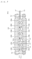
- FIG.7 is a sectional view showing the structure of an IGBT module 500 of the fifth preferred embodiment.
- This preferred embodiment shows an uninsulated type semiconductor module, which has a case 50 composed of conductive radiation boards 50a and 50b serving as collector electrode plates.
- the case 50 includes the radiation boards 50a and 50b composed of two metal plates.
- IGBT devices 28e and diode devices 29c as the first semiconductor devices, and IGBT devices 28f and diode devices 29d as the second semiconductor devices, are stacked in such a way that their emitter electrode 30 surfaces and the anode electrode 33 surfaces face to each other through a module emitter electrode 51 as the element connecting conductor.
- the IGBT devices and the diode devices are arranged between the two radiation boards 50a and 50b, and the radiation boards 50a and 50b pressurize the stacked devices 28e and 28f, and 29c and 29d.
- Pressurizing bolts 52 are used to pressurize with the radiation boards 50a and 50b.
- the pressurizing bolts 52 fix the radiation boards 50a and 50b and exert pressure to ensure the electric junction and thermal junction between the devices 28e, 28f, 29c, and 29d and the radiation boards 50a and 50b (the collector electrode plates), and the module emitter electrode 51.
- the gate electrodes 31 of the IGBT devices 28e and 28f in the module are connected to the gate terminal 47 of the module through gate pins 42a.
- two IGBT devices 28e and 28f, and two diode devices 29c and 29d are vertically stacked and joined, with the module emitter electrode 51 as the element connecting conductor interposed therebetween. This reduces the area of the module approximately half, thus further effectively achieving the size reduction. Furthermore, the current flows uniformly in the circuit including the upper devices 28f and 29d and in the circuit including the lower devices 28e and 29c, which provides a reliable module with stable characteristics.
- the module provides remarkable cooling performance since all device 28e, 28f, 29c, and 29d are in contact with the two radiation boards 50a and 50b in their surfaces.
- module emitter electrode 51 and the devices 28e, 28f, 29c, and 29d are joined by using pressurizing force. This eliminates the need of processing with solder or conductive resin and simplifies the manufacturing process.
- the contact between the devices 28e, 28f, 29c, 29d and the radiation boards 50a, 50b is made by mechanical pressure, too.
- the contact surfaces between the radiation boards 50a and 50b and the devices 28e, 28f, 29c, 29d may be bonded together with a conductive bonding material like solder, in which case the bonded surfaces between the module emitter electrode 51 and the devices 28e, 28f, 29c, 29d are bonded with pressure. This simplifies the assembly of the module.
Landscapes
- Cooling Or The Like Of Semiconductors Or Solid State Devices (AREA)
- Inverter Devices (AREA)
Priority Applications (1)
| Application Number | Priority Date | Filing Date | Title |
|---|---|---|---|
| EP20070023994 EP1914805A3 (fr) | 1998-11-30 | 1999-11-29 | Module semi-conducteur |
Applications Claiming Priority (2)
| Application Number | Priority Date | Filing Date | Title |
|---|---|---|---|
| JP33954398 | 1998-11-30 | ||
| JP33954398A JP2000164800A (ja) | 1998-11-30 | 1998-11-30 | 半導体モジュール |
Related Child Applications (2)
| Application Number | Title | Priority Date | Filing Date |
|---|---|---|---|
| EP20070023994 Division EP1914805A3 (fr) | 1998-11-30 | 1999-11-29 | Module semi-conducteur |
| EP07023994.2 Division-Into | 2007-12-11 |
Publications (3)
| Publication Number | Publication Date |
|---|---|
| EP1006578A2 true EP1006578A2 (fr) | 2000-06-07 |
| EP1006578A3 EP1006578A3 (fr) | 2000-11-08 |
| EP1006578B1 EP1006578B1 (fr) | 2011-02-16 |
Family
ID=18328479
Family Applications (2)
| Application Number | Title | Priority Date | Filing Date |
|---|---|---|---|
| EP20070023994 Withdrawn EP1914805A3 (fr) | 1998-11-30 | 1999-11-29 | Module semi-conducteur |
| EP19990123702 Expired - Lifetime EP1006578B1 (fr) | 1998-11-30 | 1999-11-29 | Module semiconducteur de puissance |
Family Applications Before (1)
| Application Number | Title | Priority Date | Filing Date |
|---|---|---|---|
| EP20070023994 Withdrawn EP1914805A3 (fr) | 1998-11-30 | 1999-11-29 | Module semi-conducteur |
Country Status (4)
| Country | Link |
|---|---|
| US (1) | US6836006B2 (fr) |
| EP (2) | EP1914805A3 (fr) |
| JP (1) | JP2000164800A (fr) |
| DE (1) | DE69943196D1 (fr) |
Cited By (7)
| Publication number | Priority date | Publication date | Assignee | Title |
|---|---|---|---|---|
| WO2002013260A3 (fr) * | 2000-08-10 | 2002-04-25 | Infineon Technologies Ag | Circuit comprenant au moins deux corps semi-conducteurs et un corps de refroidissement |
| DE10301091A1 (de) * | 2003-01-14 | 2004-07-22 | Infineon Technologies Ag | Leistungs-Halbleiterbauelement, Multichip-Anordnung und Verfahren zur Verbindung von einem gemeinsamen Substratträger zugeordneten Halbleitereinrichtung |
| DE10113967B4 (de) * | 2000-07-28 | 2008-08-21 | Mitsubishi Denki K.K. | Leistungsmodule |
| CN102254881A (zh) * | 2010-05-20 | 2011-11-23 | 三菱电机株式会社 | 半导体装置 |
| CN105405813A (zh) * | 2014-09-08 | 2016-03-16 | 罗伯特·博世有限公司 | 电子构件 |
| CN111816648A (zh) * | 2019-04-12 | 2020-10-23 | 三菱电机株式会社 | 半导体装置 |
| CN112928089A (zh) * | 2021-01-29 | 2021-06-08 | 西安理工大学 | 一种减小高压SiC模块位移电流的结构 |
Families Citing this family (33)
| Publication number | Priority date | Publication date | Assignee | Title |
|---|---|---|---|---|
| JP2003258178A (ja) * | 2002-02-27 | 2003-09-12 | Sanyo Electric Co Ltd | 半導体装置 |
| JP3958156B2 (ja) | 2002-08-30 | 2007-08-15 | 三菱電機株式会社 | 電力用半導体装置 |
| US7015570B2 (en) * | 2002-12-09 | 2006-03-21 | International Business Machines Corp. | Electronic substrate with inboard terminal array, perimeter terminal array and exterior terminal array on a second surface and module and system including the substrate |
| US6995473B2 (en) * | 2002-12-19 | 2006-02-07 | Matsushita Electric Industrial Co., Ltd. | Stacked semiconductor transistors |
| US7005734B2 (en) * | 2003-05-05 | 2006-02-28 | Ixys Corporation | Double-sided cooling isolated packaged power semiconductor device |
| JP4164409B2 (ja) * | 2003-06-13 | 2008-10-15 | 三菱電機株式会社 | 半導体パワーモジュール |
| JPWO2005018001A1 (ja) * | 2003-08-18 | 2007-10-04 | サンケン電気株式会社 | 半導体装置 |
| JP4323299B2 (ja) * | 2003-12-03 | 2009-09-02 | 三菱電機株式会社 | 半導体装置 |
| JP4179292B2 (ja) * | 2005-02-21 | 2008-11-12 | サンケン電気株式会社 | 半導体装置 |
| FR2888460B1 (fr) * | 2005-07-08 | 2010-12-24 | Valeo Vision | Dispositif d'eclairage et/ou de signalisation pour vehicule, associe a une electronique de haut niveau d'integration |
| US20070051535A1 (en) * | 2005-09-02 | 2007-03-08 | Hon Hai Precision Industry Co., Ltd. | Circuit board assembly and electronic device utilizing the same |
| JP4707548B2 (ja) * | 2005-12-08 | 2011-06-22 | 富士通セミコンダクター株式会社 | 半導体装置、及び半導体装置の製造方法 |
| DE102006008632B4 (de) * | 2006-02-21 | 2007-11-15 | Infineon Technologies Ag | Leistungshalbleiterbauteil und Verfahren zu dessen Herstellung |
| CN2919782Y (zh) * | 2006-03-23 | 2007-07-04 | 鸿富锦精密工业(深圳)有限公司 | 逆变器及其整合式印刷电路板 |
| US7554188B2 (en) * | 2006-04-13 | 2009-06-30 | International Rectifier Corporation | Low inductance bond-wireless co-package for high power density devices, especially for IGBTs and diodes |
| KR101255334B1 (ko) * | 2006-05-08 | 2013-04-16 | 페어차일드코리아반도체 주식회사 | 저 열저항 파워 모듈 및 그 제조방법 |
| JP4943373B2 (ja) * | 2008-05-09 | 2012-05-30 | 新日本製鐵株式会社 | デバイス実装方法 |
| JP5339800B2 (ja) * | 2008-07-10 | 2013-11-13 | 三菱電機株式会社 | 半導体装置の製造方法 |
| JP4803241B2 (ja) | 2008-11-27 | 2011-10-26 | 三菱電機株式会社 | 半導体モジュール |
| JP2011009767A (ja) * | 2010-08-17 | 2011-01-13 | Renesas Electronics Corp | 半導体装置 |
| US8963338B2 (en) * | 2011-03-02 | 2015-02-24 | International Rectifier Corporation | III-nitride transistor stacked with diode in a package |
| KR101301387B1 (ko) | 2011-09-16 | 2013-08-28 | 삼성전기주식회사 | 전력 반도체 모듈 |
| WO2013118415A1 (fr) * | 2012-02-09 | 2013-08-15 | 富士電機株式会社 | Dispositif à semiconducteur |
| KR101388737B1 (ko) * | 2012-04-12 | 2014-04-25 | 삼성전기주식회사 | 반도체 패키지, 반도체 모듈, 및 그 실장 구조 |
| US9385111B2 (en) * | 2013-11-22 | 2016-07-05 | Infineon Technologies Austria Ag | Electronic component with electronic chip between redistribution structure and mounting structure |
| CN107851634B (zh) * | 2015-05-22 | 2020-06-30 | Abb电网瑞士股份公司 | 功率半导体模块 |
| DE112016007133B4 (de) * | 2016-08-10 | 2021-08-12 | Mitsubishi Electric Corporation | Halbleitervorrichtung |
| JP2018064362A (ja) * | 2016-10-12 | 2018-04-19 | 学校法人早稲田大学 | 半導体装置 |
| EP3389090A1 (fr) | 2017-04-11 | 2018-10-17 | ABB Schweiz AG | Module électronique de puissance |
| US11189591B2 (en) | 2017-05-19 | 2021-11-30 | Shindengen Electric Manufacturing Co., Ltd. | Electronic module |
| JP6919392B2 (ja) * | 2017-07-26 | 2021-08-18 | 株式会社デンソー | 半導体モジュール |
| JP7069787B2 (ja) * | 2018-02-09 | 2022-05-18 | 株式会社デンソー | 半導体装置 |
| US20230136604A1 (en) * | 2020-03-31 | 2023-05-04 | Sumitomo Electric Industries, Ltd. | Semiconductor device |
Citations (2)
| Publication number | Priority date | Publication date | Assignee | Title |
|---|---|---|---|---|
| US4878106A (en) | 1986-12-02 | 1989-10-31 | Anton Piller Gmbh & Co. Kg | Semiconductor circuit packages for use in high power applications and method of making the same |
| US5532512A (en) | 1994-10-03 | 1996-07-02 | General Electric Company | Direct stacked and flip chip power semiconductor device structures |
Family Cites Families (17)
| Publication number | Priority date | Publication date | Assignee | Title |
|---|---|---|---|---|
| US4122479A (en) * | 1975-01-31 | 1978-10-24 | Hitachi, Ltd. | Optoelectronic device having control circuit for light emitting element and circuit for light receiving element integrated in a semiconductor body |
| JPS57177551A (en) * | 1981-04-27 | 1982-11-01 | Hitachi Ltd | Semiconductor device and manufacturing method therefor |
| JPS58121661A (ja) * | 1982-01-13 | 1983-07-20 | Hitachi Ltd | 半導体装置 |
| JPS58122661A (ja) | 1982-01-18 | 1983-07-21 | Pioneer Electronic Corp | レコ−ドプレ−ヤにおける曲間検出装置 |
| US4963976A (en) * | 1988-09-12 | 1990-10-16 | Sundstrand Corporation | Integrated electrical conducting, cooling and clamping assembly for power semiconductors |
| JPH06181286A (ja) * | 1992-12-14 | 1994-06-28 | Toshiba Corp | 半導体装置 |
| JP2991010B2 (ja) * | 1993-09-29 | 1999-12-20 | 富士電機株式会社 | 半導体装置およびその製造方法 |
| US5478700A (en) * | 1993-12-21 | 1995-12-26 | International Business Machines Corporation | Method for applying bonding agents to pad and/or interconnection sites in the manufacture of electrical circuits using a bonding agent injection head |
| DE4421319A1 (de) * | 1994-06-17 | 1995-12-21 | Abb Management Ag | Niederinduktives Leistungshalbleitermodul |
| JP3206717B2 (ja) * | 1996-04-02 | 2001-09-10 | 富士電機株式会社 | 電力用半導体モジュール |
| US6075279A (en) * | 1996-06-26 | 2000-06-13 | Sanyo Electric Co., Ltd. | Semiconductor device |
| SE520788C2 (sv) | 1997-03-24 | 2003-08-26 | Abb Ab | VSC-strömriktare |
| DE69832359T2 (de) * | 1997-07-19 | 2006-08-03 | Koninklijke Philips Electronics N.V. | Halbleitervorrichtung -anordnung und -schaltungen |
| CA2218307C (fr) * | 1997-10-10 | 2006-01-03 | Gennum Corporation | Configuration d'encapsulation 3-d pour module multipuce |
| US6081039A (en) * | 1997-12-05 | 2000-06-27 | International Rectifier Corporation | Pressure assembled motor cube |
| US6201701B1 (en) * | 1998-03-11 | 2001-03-13 | Kimball International, Inc. | Integrated substrate with enhanced thermal characteristics |
| US6586835B1 (en) * | 1998-08-31 | 2003-07-01 | Micron Technology, Inc. | Compact system module with built-in thermoelectric cooling |
-
1998
- 1998-11-30 JP JP33954398A patent/JP2000164800A/ja active Pending
-
1999
- 1999-11-29 EP EP20070023994 patent/EP1914805A3/fr not_active Withdrawn
- 1999-11-29 EP EP19990123702 patent/EP1006578B1/fr not_active Expired - Lifetime
- 1999-11-29 US US09/447,945 patent/US6836006B2/en not_active Expired - Fee Related
- 1999-11-29 DE DE69943196T patent/DE69943196D1/de not_active Expired - Lifetime
Patent Citations (2)
| Publication number | Priority date | Publication date | Assignee | Title |
|---|---|---|---|---|
| US4878106A (en) | 1986-12-02 | 1989-10-31 | Anton Piller Gmbh & Co. Kg | Semiconductor circuit packages for use in high power applications and method of making the same |
| US5532512A (en) | 1994-10-03 | 1996-07-02 | General Electric Company | Direct stacked and flip chip power semiconductor device structures |
Cited By (9)
| Publication number | Priority date | Publication date | Assignee | Title |
|---|---|---|---|---|
| DE10113967B4 (de) * | 2000-07-28 | 2008-08-21 | Mitsubishi Denki K.K. | Leistungsmodule |
| WO2002013260A3 (fr) * | 2000-08-10 | 2002-04-25 | Infineon Technologies Ag | Circuit comprenant au moins deux corps semi-conducteurs et un corps de refroidissement |
| DE10301091A1 (de) * | 2003-01-14 | 2004-07-22 | Infineon Technologies Ag | Leistungs-Halbleiterbauelement, Multichip-Anordnung und Verfahren zur Verbindung von einem gemeinsamen Substratträger zugeordneten Halbleitereinrichtung |
| DE10301091B4 (de) * | 2003-01-14 | 2015-01-22 | Infineon Technologies Ag | Leistungs-Halbleiterbauelement und Verfahren zur Verbindung von einem gemeinsamen Substratträger zugeordneten Halbleitereinrichtungen |
| CN102254881A (zh) * | 2010-05-20 | 2011-11-23 | 三菱电机株式会社 | 半导体装置 |
| CN105405813A (zh) * | 2014-09-08 | 2016-03-16 | 罗伯特·博世有限公司 | 电子构件 |
| CN105405813B (zh) * | 2014-09-08 | 2020-01-21 | 罗伯特·博世有限公司 | 电子构件 |
| CN111816648A (zh) * | 2019-04-12 | 2020-10-23 | 三菱电机株式会社 | 半导体装置 |
| CN112928089A (zh) * | 2021-01-29 | 2021-06-08 | 西安理工大学 | 一种减小高压SiC模块位移电流的结构 |
Also Published As
| Publication number | Publication date |
|---|---|
| EP1006578B1 (fr) | 2011-02-16 |
| US20020043708A1 (en) | 2002-04-18 |
| US6836006B2 (en) | 2004-12-28 |
| EP1914805A3 (fr) | 2008-05-28 |
| EP1006578A3 (fr) | 2000-11-08 |
| EP1914805A2 (fr) | 2008-04-23 |
| DE69943196D1 (de) | 2011-03-31 |
| JP2000164800A (ja) | 2000-06-16 |
Similar Documents
| Publication | Publication Date | Title |
|---|---|---|
| US6836006B2 (en) | Semiconductor module | |
| KR100430772B1 (ko) | 반도체장치 | |
| US6703703B2 (en) | Low cost power semiconductor module without substrate | |
| US5767573A (en) | Semiconductor device | |
| CN104303297B (zh) | 电力用半导体模块 | |
| US6946740B2 (en) | High power MCM package | |
| CN1855476B (zh) | 半导体装置 | |
| CN109428498B (zh) | 组件结构、功率模块及功率模块组装结构 | |
| US11456244B2 (en) | Semiconductor device | |
| JP2003197864A (ja) | パワー半導体モジュール | |
| EP1378941B1 (fr) | Module semi-conductrice et convertisseur à haut prestation | |
| CN111095760A (zh) | 电力转换装置 | |
| US20240404977A1 (en) | Semiconductor device and semiconductor module | |
| EP1768243A1 (fr) | Dispositif inverseur | |
| JP3673776B2 (ja) | 半導体モジュール及び電力変換装置 | |
| JP4096741B2 (ja) | 半導体装置 | |
| JP3529675B2 (ja) | 半導体装置及びインバータ装置 | |
| JP2019050301A (ja) | パワー半導体モジュール | |
| US6559532B1 (en) | Matrix converter | |
| CN115380377A (zh) | 半导体模块 | |
| US6081039A (en) | Pressure assembled motor cube | |
| JP7781340B2 (ja) | パワー半導体装置、パワーモジュール及び電力変換装置 | |
| JP2001085612A (ja) | 相補型igbtの実装構造 | |
| JP7651289B2 (ja) | パワー半導体モジュール及びその製造方法並びに電力変換装置 | |
| JP2019161124A (ja) | 半導体装置 |
Legal Events
| Date | Code | Title | Description |
|---|---|---|---|
| PUAI | Public reference made under article 153(3) epc to a published international application that has entered the european phase |
Free format text: ORIGINAL CODE: 0009012 |
|
| AK | Designated contracting states |
Kind code of ref document: A2 Designated state(s): CH DE FR GB IT LI |
|
| AX | Request for extension of the european patent |
Free format text: AL;LT;LV;MK;RO;SI |
|
| PUAL | Search report despatched |
Free format text: ORIGINAL CODE: 0009013 |
|
| AK | Designated contracting states |
Kind code of ref document: A3 Designated state(s): AT BE CH CY DE DK ES FI FR GB GR IE IT LI LU MC NL PT SE |
|
| AX | Request for extension of the european patent |
Free format text: AL;LT;LV;MK;RO;SI |
|
| 17P | Request for examination filed |
Effective date: 20001117 |
|
| 17Q | First examination report despatched |
Effective date: 20010309 |
|
| AKX | Designation fees paid |
Free format text: CH DE FR GB IT LI |
|
| RAP1 | Party data changed (applicant data changed or rights of an application transferred) |
Owner name: MITSUBISHI DENKI KABUSHIKI KAISHA |
|
| GRAP | Despatch of communication of intention to grant a patent |
Free format text: ORIGINAL CODE: EPIDOSNIGR1 |
|
| GRAS | Grant fee paid |
Free format text: ORIGINAL CODE: EPIDOSNIGR3 |
|
| GRAA | (expected) grant |
Free format text: ORIGINAL CODE: 0009210 |
|
| AK | Designated contracting states |
Kind code of ref document: B1 Designated state(s): CH DE FR GB IT LI |
|
| REG | Reference to a national code |
Ref country code: GB Ref legal event code: FG4D |
|
| REG | Reference to a national code |
Ref country code: CH Ref legal event code: EP |
|
| REF | Corresponds to: |
Ref document number: 69943196 Country of ref document: DE Date of ref document: 20110331 Kind code of ref document: P |
|
| REG | Reference to a national code |
Ref country code: DE Ref legal event code: R096 Ref document number: 69943196 Country of ref document: DE Effective date: 20110331 |
|
| PLBE | No opposition filed within time limit |
Free format text: ORIGINAL CODE: 0009261 |
|
| STAA | Information on the status of an ep patent application or granted ep patent |
Free format text: STATUS: NO OPPOSITION FILED WITHIN TIME LIMIT |
|
| 26N | No opposition filed |
Effective date: 20111117 |
|
| REG | Reference to a national code |
Ref country code: DE Ref legal event code: R097 Ref document number: 69943196 Country of ref document: DE Effective date: 20111117 |
|
| PG25 | Lapsed in a contracting state [announced via postgrant information from national office to epo] |
Ref country code: IT Free format text: LAPSE BECAUSE OF FAILURE TO SUBMIT A TRANSLATION OF THE DESCRIPTION OR TO PAY THE FEE WITHIN THE PRESCRIBED TIME-LIMIT Effective date: 20110216 |
|
| REG | Reference to a national code |
Ref country code: CH Ref legal event code: PL |
|
| GBPC | Gb: european patent ceased through non-payment of renewal fee |
Effective date: 20111129 |
|
| PG25 | Lapsed in a contracting state [announced via postgrant information from national office to epo] |
Ref country code: CH Free format text: LAPSE BECAUSE OF NON-PAYMENT OF DUE FEES Effective date: 20111130 Ref country code: LI Free format text: LAPSE BECAUSE OF NON-PAYMENT OF DUE FEES Effective date: 20111130 |
|
| PG25 | Lapsed in a contracting state [announced via postgrant information from national office to epo] |
Ref country code: GB Free format text: LAPSE BECAUSE OF NON-PAYMENT OF DUE FEES Effective date: 20111129 |
|
| PGFP | Annual fee paid to national office [announced via postgrant information from national office to epo] |
Ref country code: FR Payment date: 20121130 Year of fee payment: 14 |
|
| REG | Reference to a national code |
Ref country code: DE Ref legal event code: R119 Ref document number: 69943196 Country of ref document: DE Effective date: 20130601 |
|
| PG25 | Lapsed in a contracting state [announced via postgrant information from national office to epo] |
Ref country code: DE Free format text: LAPSE BECAUSE OF NON-PAYMENT OF DUE FEES Effective date: 20130601 |
|
| REG | Reference to a national code |
Ref country code: FR Ref legal event code: ST Effective date: 20140731 |
|
| PG25 | Lapsed in a contracting state [announced via postgrant information from national office to epo] |
Ref country code: FR Free format text: LAPSE BECAUSE OF NON-PAYMENT OF DUE FEES Effective date: 20131202 |