EP1006588A2 - Elektrolumineszenz-Farbanzeigevorrichtung - Google Patents
Elektrolumineszenz-Farbanzeigevorrichtung Download PDFInfo
- Publication number
- EP1006588A2 EP1006588A2 EP99309646A EP99309646A EP1006588A2 EP 1006588 A2 EP1006588 A2 EP 1006588A2 EP 99309646 A EP99309646 A EP 99309646A EP 99309646 A EP99309646 A EP 99309646A EP 1006588 A2 EP1006588 A2 EP 1006588A2
- Authority
- EP
- European Patent Office
- Prior art keywords
- capacitor
- thin film
- film transistor
- tft
- display device
- Prior art date
- Legal status (The legal status is an assumption and is not a legal conclusion. Google has not performed a legal analysis and makes no representation as to the accuracy of the status listed.)
- Withdrawn
Links
Images


Classifications
-
- H—ELECTRICITY
- H10—SEMICONDUCTOR DEVICES; ELECTRIC SOLID-STATE DEVICES NOT OTHERWISE PROVIDED FOR
- H10K—ORGANIC ELECTRIC SOLID-STATE DEVICES
- H10K59/00—Integrated devices, or assemblies of multiple devices, comprising at least one organic light-emitting element covered by group H10K50/00
- H10K59/10—OLED displays
- H10K59/12—Active-matrix OLED [AMOLED] displays
- H10K59/121—Active-matrix OLED [AMOLED] displays characterised by the geometry or disposition of pixel elements
- H10K59/1213—Active-matrix OLED [AMOLED] displays characterised by the geometry or disposition of pixel elements the pixel elements being TFTs
-
- H—ELECTRICITY
- H05—ELECTRIC TECHNIQUES NOT OTHERWISE PROVIDED FOR
- H05B—ELECTRIC HEATING; ELECTRIC LIGHT SOURCES NOT OTHERWISE PROVIDED FOR; CIRCUIT ARRANGEMENTS FOR ELECTRIC LIGHT SOURCES, IN GENERAL
- H05B33/00—Electroluminescent light sources
-
- G—PHYSICS
- G09—EDUCATION; CRYPTOGRAPHY; DISPLAY; ADVERTISING; SEALS
- G09G—ARRANGEMENTS OR CIRCUITS FOR CONTROL OF INDICATING DEVICES USING STATIC MEANS TO PRESENT VARIABLE INFORMATION
- G09G3/00—Control arrangements or circuits, of interest only in connection with visual indicators other than cathode-ray tubes
- G09G3/20—Control arrangements or circuits, of interest only in connection with visual indicators other than cathode-ray tubes for presentation of an assembly of a number of characters, e.g. a page, by composing the assembly by combination of individual elements arranged in a matrix no fixed position being assigned to or needed to be assigned to the individual characters or partial characters
- G09G3/22—Control arrangements or circuits, of interest only in connection with visual indicators other than cathode-ray tubes for presentation of an assembly of a number of characters, e.g. a page, by composing the assembly by combination of individual elements arranged in a matrix no fixed position being assigned to or needed to be assigned to the individual characters or partial characters using controlled light sources
- G09G3/30—Control arrangements or circuits, of interest only in connection with visual indicators other than cathode-ray tubes for presentation of an assembly of a number of characters, e.g. a page, by composing the assembly by combination of individual elements arranged in a matrix no fixed position being assigned to or needed to be assigned to the individual characters or partial characters using controlled light sources using electroluminescent panels
- G09G3/32—Control arrangements or circuits, of interest only in connection with visual indicators other than cathode-ray tubes for presentation of an assembly of a number of characters, e.g. a page, by composing the assembly by combination of individual elements arranged in a matrix no fixed position being assigned to or needed to be assigned to the individual characters or partial characters using controlled light sources using electroluminescent panels semiconductive, e.g. using light-emitting diodes [LED]
- G09G3/3208—Control arrangements or circuits, of interest only in connection with visual indicators other than cathode-ray tubes for presentation of an assembly of a number of characters, e.g. a page, by composing the assembly by combination of individual elements arranged in a matrix no fixed position being assigned to or needed to be assigned to the individual characters or partial characters using controlled light sources using electroluminescent panels semiconductive, e.g. using light-emitting diodes [LED] organic, e.g. using organic light-emitting diodes [OLED]
- G09G3/3225—Control arrangements or circuits, of interest only in connection with visual indicators other than cathode-ray tubes for presentation of an assembly of a number of characters, e.g. a page, by composing the assembly by combination of individual elements arranged in a matrix no fixed position being assigned to or needed to be assigned to the individual characters or partial characters using controlled light sources using electroluminescent panels semiconductive, e.g. using light-emitting diodes [LED] organic, e.g. using organic light-emitting diodes [OLED] using an active matrix
-
- H—ELECTRICITY
- H10—SEMICONDUCTOR DEVICES; ELECTRIC SOLID-STATE DEVICES NOT OTHERWISE PROVIDED FOR
- H10K—ORGANIC ELECTRIC SOLID-STATE DEVICES
- H10K59/00—Integrated devices, or assemblies of multiple devices, comprising at least one organic light-emitting element covered by group H10K50/00
- H10K59/10—OLED displays
- H10K59/12—Active-matrix OLED [AMOLED] displays
- H10K59/121—Active-matrix OLED [AMOLED] displays characterised by the geometry or disposition of pixel elements
- H10K59/1216—Active-matrix OLED [AMOLED] displays characterised by the geometry or disposition of pixel elements the pixel elements being capacitors
-
- H—ELECTRICITY
- H10—SEMICONDUCTOR DEVICES; ELECTRIC SOLID-STATE DEVICES NOT OTHERWISE PROVIDED FOR
- H10K—ORGANIC ELECTRIC SOLID-STATE DEVICES
- H10K59/00—Integrated devices, or assemblies of multiple devices, comprising at least one organic light-emitting element covered by group H10K50/00
- H10K59/30—Devices specially adapted for multicolour light emission
- H10K59/35—Devices specially adapted for multicolour light emission comprising red-green-blue [RGB] subpixels
-
- G—PHYSICS
- G09—EDUCATION; CRYPTOGRAPHY; DISPLAY; ADVERTISING; SEALS
- G09G—ARRANGEMENTS OR CIRCUITS FOR CONTROL OF INDICATING DEVICES USING STATIC MEANS TO PRESENT VARIABLE INFORMATION
- G09G2300/00—Aspects of the constitution of display devices
- G09G2300/04—Structural and physical details of display devices
- G09G2300/0404—Matrix technologies
- G09G2300/0417—Special arrangements specific to the use of low carrier mobility technology
-
- G—PHYSICS
- G09—EDUCATION; CRYPTOGRAPHY; DISPLAY; ADVERTISING; SEALS
- G09G—ARRANGEMENTS OR CIRCUITS FOR CONTROL OF INDICATING DEVICES USING STATIC MEANS TO PRESENT VARIABLE INFORMATION
- G09G2300/00—Aspects of the constitution of display devices
- G09G2300/04—Structural and physical details of display devices
- G09G2300/0421—Structural details of the set of electrodes
- G09G2300/0426—Layout of electrodes and connections
-
- G—PHYSICS
- G09—EDUCATION; CRYPTOGRAPHY; DISPLAY; ADVERTISING; SEALS
- G09G—ARRANGEMENTS OR CIRCUITS FOR CONTROL OF INDICATING DEVICES USING STATIC MEANS TO PRESENT VARIABLE INFORMATION
- G09G2300/00—Aspects of the constitution of display devices
- G09G2300/04—Structural and physical details of display devices
- G09G2300/0439—Pixel structures
- G09G2300/0465—Improved aperture ratio, e.g. by size reduction of the pixel circuit, e.g. for improving the pixel density or the maximum displayable luminance or brightness
-
- G—PHYSICS
- G09—EDUCATION; CRYPTOGRAPHY; DISPLAY; ADVERTISING; SEALS
- G09G—ARRANGEMENTS OR CIRCUITS FOR CONTROL OF INDICATING DEVICES USING STATIC MEANS TO PRESENT VARIABLE INFORMATION
- G09G2300/00—Aspects of the constitution of display devices
- G09G2300/08—Active matrix structure, i.e. with use of active elements, inclusive of non-linear two terminal elements, in the pixels together with light emitting or modulating elements
- G09G2300/0809—Several active elements per pixel in active matrix panels
- G09G2300/0842—Several active elements per pixel in active matrix panels forming a memory circuit, e.g. a dynamic memory with one capacitor
-
- G—PHYSICS
- G09—EDUCATION; CRYPTOGRAPHY; DISPLAY; ADVERTISING; SEALS
- G09G—ARRANGEMENTS OR CIRCUITS FOR CONTROL OF INDICATING DEVICES USING STATIC MEANS TO PRESENT VARIABLE INFORMATION
- G09G2320/00—Control of display operating conditions
- G09G2320/02—Improving the quality of display appearance
- G09G2320/0209—Crosstalk reduction, i.e. to reduce direct or indirect influences of signals directed to a certain pixel of the displayed image on other pixels of said image, inclusive of influences affecting pixels in different frames or fields or sub-images which constitute a same image, e.g. left and right images of a stereoscopic display
- G09G2320/0214—Crosstalk reduction, i.e. to reduce direct or indirect influences of signals directed to a certain pixel of the displayed image on other pixels of said image, inclusive of influences affecting pixels in different frames or fields or sub-images which constitute a same image, e.g. left and right images of a stereoscopic display with crosstalk due to leakage current of pixel switch in active matrix panels
-
- H—ELECTRICITY
- H10—SEMICONDUCTOR DEVICES; ELECTRIC SOLID-STATE DEVICES NOT OTHERWISE PROVIDED FOR
- H10K—ORGANIC ELECTRIC SOLID-STATE DEVICES
- H10K59/00—Integrated devices, or assemblies of multiple devices, comprising at least one organic light-emitting element covered by group H10K50/00
- H10K59/10—OLED displays
- H10K59/12—Active-matrix OLED [AMOLED] displays
- H10K59/131—Interconnections, e.g. wiring lines or terminals
Definitions
- the present invention relates to an active type color EL (electroluminescence) display device in which an electroluminescence (EL) element is driven using a thin film transistor(TFT).
- EL electroluminescence
- the first method different emissive materials for each of the primary RGB colors are used in corresponding emissive layers to individually form discrete color pixels directly emitting respective RGB light rays.
- an emissive layer generates white luminescence which is then converted into three primary colors using color filters.
- a third method is based on conversion of light from a blue emissive layer into three primary colors using color conversion mediums (CCM). As light energy is lost in the second and third methods above due to the use of color filters or color conversion mediums, the first method is the most effective of these in this respect because a desired light ray is directly emitted.
- CCM color conversion mediums
- a passive type using a passive matrix and an active type employing TFTs, are available.
- the circuit configuration shown in Fig. 1 may be used in an active display.
- Fig. 1 illustrates a circuit configuration for a single pixel in such a display pixel.
- Each pixel comprises an organic EL element 20, a first TFT 21 for switching, in which a display signal DATA is applied to a drain and a scan signal SCAN is applied to a gate to switch the TFT on and off, a capacitor 22 which is charged by a display signal DATA applied when the TFT 21 is on and which holds a charge voltage Vh when the TFT 21 is off, a second TFT 23 in which a drain is connected to a drive source of a voltage V COM , a source is connected to an anode of the organic EL element 20 and a hold voltage Vh is applied to a gate from the capacitor 22 to drive the organic EL element 20.
- a scan signal SCAN rises to an H level during one horizontal scanning period (1H).
- a display signal DATA is applied to one end of the capacitor 22, which is then charged by a voltage Vh corresponding to the display signal DATA.
- This voltage Vh remains held in the capacitor 22 for one vertical scanning period (1V) even after the signal SCAN becomes a low level to switch the TFT 21 off. Because the voltage Vh is supplied to the gate of the TFT 23, the EL element is controlled so as to emit light with a luminance in accordance with the voltage Vh.
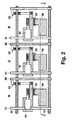
- Fig. 2 depicts a conceptual plan view showing a configuration of a related art device
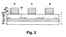
- Fig. 3 is a cross section taken along line C-C in Fig. 2.
- Each of the drawings depicts three pixels.
- numeral 50 represents a drain line for supplying a display signal DATA
- numeral 51 represents a drive source line for supplying a supply voltage V COM
- numeral 52 represents a gate line for supplying a scan signal SCAN.
- numerals 53, 54, and 55 designate features corresponding the first TFT 21, the capacitor 22, and the second TFT 23 in Fig. 1, respectively
- numeral 56 designates an anode of the EL element 20 which constitutes a pixel electrode. As shown, discrete anodes 56 are separately formed for each pixel on a planarization insulating film 60.
- a hole-transport layer 61, an emissive layer 62, an electron-transport layer 63, and a cathode 64 are sequentially laminated on the discrete anode 56, thereby forming an EL element. Holes injected from the anodes 56 and electrons injected from the cathodes 64 are recombined inside the emissive layer 62, which emits light in the direction of the transparent anodes toward outside, as shown by arrows in Fig. 3.
- discrete hole-transport layers 61, discrete emissive layers 62 and discrete electron-transport layers 63 having substantially the same shape as the discrete anodes 56 are provided for respective pixels.
- Emissive materials which are different for each RGB are used in the corresponding emissive layers 62, and therefore light rays having respective RGB colors are emitted from respective EL elements.
- the cathode 64 which applies a common voltage to each pixel, extends over the pixels.
- Partitions 68 are interposed between adjoining emissive layers 62.
- numerals 65, 66, and 67 designate a transparent glass substrate, a gate insulating film, and an interlayer insulating film, respectively.
- the arrangement of the first TFT 53, the capacitor 54, the second TFT 55, and the anode 56 of the related examples do not take sufficient consideration of integration efficiency and therefore a more highly-integrated configuration is in demand.
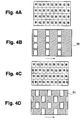
- the color display device generally adopts a stripe arrangement as shown in Fig. 4A or a delta arrangement as shown in Fig. 4C as an arrangement for three primary colors of RGB.
- a stripe arrangement shown in Fig. 4A is adopted, for example, a metal mask 70 shown in Fig. 4B may be used to form the luminescent layers as follows. First, a luminescent layer for R is formed by evaporating only an R color luminescent material onto the hole transport layer.
- the metal mask 70 is displaced by a distance corresponding to one pixel in the horizontal direction to form a luminescent layer for G by evaporating only a G color luminescent materials on the hole transport layer. Finally, the metal mask 70 is further displaced by one pixel in the horizontal direction to form a luminescent layer for B by evaporating only a B color luminescent material.
- the luminescent layers can be similarly formed using the metal mask shown in Fig. 4D.
- the present invention provides a color display device suitable for a highly integrated configuration.
- a first thin film transistor is disposed in a region between a gate line and a capacitor, and a second thin film transistor is disposed in a region between the capacitor and an EL element.
- This configuration allows the capacitor, the first thin film transistor, and the second thin film transistors to be densely arranged, thereby facilitating formation of a highly integrated configuration.
- said first thin film transistor is connected to one end of one electrode of said capacitor while a gate of said second thin film transistor is connected to the other end which is opposed to said one end of the capacitor.
- the first thin film transistor and the gate of the second thin film transistor are electrically connected via the one electrode of the capacitor.
- the capacitor includes a dent region in which the first thin film transistor is disposed.
- the EL element includes a dent region in which the second thin film transistor is disposed.
- the capacitor and the EL element are disposed so as to adjoin each other in the column direction, such that space is provided in the vertical direction. Therefore, when forming a pixel electrode (for example, an anode), color mixture among adjoining pixels can be prevented , when metal mask positioning accuracy is low, thereby maintaining preferable color purity for even highly detailed displays.
- a pixel electrode for example, an anode
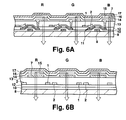
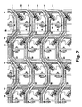
- Fig. 5 is a plan view showing a color EL display device in accordance with a first embodiment of the present invention, and depicts the configuration corresponding to three pixels of RGB. Further, Fig. 6A is a cross section taken along a line A-A of Fig. 5, and Fig. 6B is a cross section taken along a line B-B of Fig. 5. This embodiment exemplifies a configuration for the stripe pixel arrangement shown in Fig. 4A.
- a driving circuit for each pixel in this embodiment is the same as that in Fig. 1, and the configuration of the device differs from the example shown in Figs. 2 and 3 in the pattern arrangement and the cross section.
- the device comprises a data line 1 made of aluminum for supplying a display signal DATA, a power supply line 2 made of aluminum for supplying a power from a drive source COM, and a gate line made of chrome for supplying a scan signal SCAN.
- Each pixel of the EL display further comprises a first TFT 4 corresponding to the first TFT 21 in Fig. 1, a capacitor 5 corresponding to the capacitor 22 in Fig. 1, a second TFT 6 corresponding to the second TFT 23 in Fig. 1, and an anode (a first electrode) 7 of the EL element 20 comprising ITO and constituting an pixel electrode.
- regions enclosed by dot lines are formed by chromium
- regions enclosed by chain lines are formed by ITO
- regions enclosed by solid lines other than the data line 1 and the power supply line 2 are formed using a polysilicon thin film.
- the second TFT 6 is formed as follows. First, a gate electrode 9 is formed on a transparent glass substrate 8, and a gate insulating film 10 is formed thereupon. Then, a polysilicon thin film 11 formed on the gate insulating film 10 is covered with an interlayer insulating film 12, on which the data line 1 and the power supply line 2 are formed. A planarization insulating film 13 is further formed thereon and the anode 7 comprising ITO is finally formed on the planarization insulating film 13. Then, the drain region of the polysilicon thin film 11 is brought into contact with the power supply line 2 while the source region of the polysilicon thin film 11 is brought into contact with the anode 7.
- the configuration of the first TFT 4 is substantially the same as that of the second TFT 6, with the notable exception that the drain region of the first TFT 4 is connected to the data line 1, and not to the power supply line 2. Further, the capacitor 5 connected to the first TFT 4 comprises a chromium electrode and a polysilicon thin film having a gate insulating film interposed therebetween.
- the discrete anodes 7 are formed on the planarization insulating film 13 corresponding to respective pixels, and a hole-transport layer 14 is formed thereon so as to cover the entire pixels. Then, discrete emissive layers 15 are formed for each pixel, on which an electron-transport layer 16 and a cathode 17 are laminated in this order to complete formation of an EL element. Holes injected from the anode 7 and electrons injected from the cathode 17 are recombined inside the emissive layer 15, which emits light in the direction of the transparent anode toward outside, as indicated by arrows in Fig. 6A and 6B. The discrete emissive layers 15 are formed for respective pixels to have substantially the same shape as the discrete anodes 7, and different emissive materials are used for each of the RGB colors. Thus, each EL element emits one type of RGB light.
- Materials of, for example, MTDATA, Alq 3 , and MgIn alloy may be used for the hole-transport layer 14, the electron-transport layer 16, and the cathode 17, respectively.
- Alq containing DCM type as dopant is used for the emissive layer 15 for R
- Alq containing quinacridon as dopant is used for the emissive layer 15 for G
- DPVBi containing distyrylarylene or Perylene as dopant is used in the emissive layer 15 for B.
- the first TFT 4 is disposed in a region between the gate line 3 and the capacitor 5, and the capacitor 5 includes a dent region in which the first TFT 4 is disposed.
- the dent region is formed by removing a corner portion of a rectangular shape (capacitor 5).
- the opposite corner portion of the rectangular shape (capacitor 5) is also removed.
- the second TFT 6 is disposed in a region between the capacitor 5 and the anode 7, and the anode includes a dent region in which the second TFT 6 is disposed.
- the dent region is formed by removing a corner portion of a rectangular shape (anode 7).
- the capacitor 5 also functions as a wiring for connecting the source of the first TFT 4 and the gate electrode of the second TFT 6. Due to such configuration, it is possible to densely arrange the first TFT 4, the capacitor 5, the second TFT 6, and the anode 7, thereby increasing the integration efficiency of pixels to achieve highly detailed display.
- Fig. 7 depicts, in plan view, the second embodiment of the present invention.
- numeral 4 denotes a first TFT corresponding to the first TFT 21 of Fig. 5
- numeral 5 denotes a capacitor corresponding to the capacitor 22 of Fig. 3
- numeral 6 denotes a second TFT corresponding to the second TFT 23 of Fig. 3
- numeral 7 denotes an anode of the EL element 20 comprising ITO and constituting a pixel electrode.
- This embodiment exemplifies a configuration in the case of a delta pixel arrangement as shown in Fig. 4C.
- the first TFT 4 is disposed in a region between the gate line 3 and the capacitor 5, and the capacitor 5 includes a dent region in which the first TFT 4 is disposed.
- the second TFT 6 is disposed in a region between the capacitor 5 and the anode 7, and the anode 7 includes a dent region in which the second TFT 6 is disposed.
- the capacitor 5 also functions as a wiring for connecting the first TFT 4 and the second TFT 6. Due to such configuration, it is possible to densely arrange the first TFT 4, the capacitor 5, the second TFT 6, and the anode 7, thereby increasing the integration efficiency of pixels and achieving a highly detailed display.
- pixels of different colors adjoin with one another in the column direction, as shown in Fig. 4C.
- the first TFT 4 and the capacitor 5 are disposed in the vertical direction of the anode 7 which is a pixel electrode, gaps between the EL elements in the column direction can be sufficiently secured.
- the luminescent region of a pixel and the pixel electrode itself also have substantially the same shape.
- pixels of the same color which are adjacent in the column direction are displaced from each other in the row direction by a distance corresponding to about 1.5 pixels. Therefore, the arrangement including such an 1.5 pixel displacement is preferably used in the present invention.
- the size of pixel displacement is not limited to 1.5 and the arrangement including an 1.2 pixel displacement as shown in Fig. 7 may be used.
- the first thin film transistor is disposed between the gate line and the capacitor and the second thin film transistor is disposed between the capacitor and the EL element, it is possible to densely arrange these features so as to achieve a highly integrated configuration.
- color mixture in adjoining pixels which causes deterioration of color purity can be prevented in an active type color EL display device, thereby maintaining preferable color purity even in a highly detailed display.
- a room is provided in each pixel in the horizontal direction such that highly detailed display can be achieved even if accuracy in metal mask positioning is low.
- the present invention is also applicable to a delta pixel arrangement, the above-mentioned effects especially work in a stripe arrangement.
Landscapes
- Engineering & Computer Science (AREA)
- Physics & Mathematics (AREA)
- Geometry (AREA)
- Microelectronics & Electronic Packaging (AREA)
- Computer Hardware Design (AREA)
- General Physics & Mathematics (AREA)
- Theoretical Computer Science (AREA)
- Electroluminescent Light Sources (AREA)
- Devices For Indicating Variable Information By Combining Individual Elements (AREA)
Applications Claiming Priority (4)
| Application Number | Priority Date | Filing Date | Title |
|---|---|---|---|
| JP34186098 | 1998-12-01 | ||
| JP34186098 | 1998-12-01 | ||
| JP27987599 | 1999-09-30 | ||
| JP11279875A JP2000227770A (ja) | 1998-12-01 | 1999-09-30 | カラーel表示装置 |
Publications (2)
| Publication Number | Publication Date |
|---|---|
| EP1006588A2 true EP1006588A2 (de) | 2000-06-07 |
| EP1006588A3 EP1006588A3 (de) | 2005-01-05 |
Family
ID=26553522
Family Applications (1)
| Application Number | Title | Priority Date | Filing Date |
|---|---|---|---|
| EP99309646A Withdrawn EP1006588A3 (de) | 1998-12-01 | 1999-12-01 | Elektrolumineszenz-Farbanzeigevorrichtung |
Country Status (5)
| Country | Link |
|---|---|
| US (3) | US6429599B1 (de) |
| EP (1) | EP1006588A3 (de) |
| JP (1) | JP2000227770A (de) |
| KR (1) | KR20000047779A (de) |
| TW (1) | TW435054B (de) |
Cited By (6)
| Publication number | Priority date | Publication date | Assignee | Title |
|---|---|---|---|---|
| EP1298634A3 (de) * | 2001-09-28 | 2007-04-11 | SANYO ELECTRIC Co., Ltd. | Anzeigegerät mit aktiver Matrix |
| EP1594347A4 (de) * | 2003-02-13 | 2008-03-19 | Fujifilm Corp | Anzeigevorrichtung und herstellungsverfahren dafür |
| CN100414587C (zh) * | 2004-11-08 | 2008-08-27 | 三星Sdi株式会社 | 平板显示器 |
| US7633223B2 (en) | 2000-11-10 | 2009-12-15 | Semiconductor Energy Laboratory Co., Ltd. | Organic light emitting device provided with drying agent at side surfaces of a sealing member |
| US8207667B2 (en) | 2007-08-31 | 2012-06-26 | Sharp Kabushiki Kaisha | Organic EL display and manufacturing method thereof |
| US10903244B2 (en) | 2005-06-30 | 2021-01-26 | Semiconductor Energy Laboratory Co., Ltd. | Semiconductor device, display device, and electronic appliance |
Families Citing this family (45)
| Publication number | Priority date | Publication date | Assignee | Title |
|---|---|---|---|---|
| JP2000227771A (ja) * | 1998-12-01 | 2000-08-15 | Sanyo Electric Co Ltd | カラーel表示装置 |
| JP2000227770A (ja) * | 1998-12-01 | 2000-08-15 | Sanyo Electric Co Ltd | カラーel表示装置 |
| JP4530450B2 (ja) * | 1999-09-29 | 2010-08-25 | 三洋電機株式会社 | El表示装置 |
| US6774575B2 (en) * | 1999-12-22 | 2004-08-10 | Sony Corporation | Organic electroluminescence display |
| JP3902938B2 (ja) * | 2000-10-31 | 2007-04-11 | キヤノン株式会社 | 有機発光素子の製造方法及び有機発光表示体の製造方法、有機発光素子及び有機発光表示体 |
| JP4292245B2 (ja) * | 2001-02-05 | 2009-07-08 | 三星モバイルディスプレイ株式會社 | 発光体、発光素子、及び発光表示装置 |
| JP3612494B2 (ja) * | 2001-03-28 | 2005-01-19 | 株式会社日立製作所 | 表示装置 |
| KR100467943B1 (ko) * | 2001-12-28 | 2005-01-24 | 엘지.필립스 엘시디 주식회사 | 유기 전계발광소자와 그 제조방법 |
| KR100453634B1 (ko) * | 2001-12-29 | 2004-10-20 | 엘지.필립스 엘시디 주식회사 | 능동행렬 유기전기발광소자 |
| KR100489591B1 (ko) * | 2002-11-13 | 2005-05-16 | 엘지.필립스 엘시디 주식회사 | 유기전계 발광소자와 그 제조방법 |
| KR100503129B1 (ko) * | 2002-12-28 | 2005-07-22 | 엘지.필립스 엘시디 주식회사 | 듀얼패널타입 유기전계발광 소자 및 그 제조방법 |
| JP4185371B2 (ja) * | 2003-01-24 | 2008-11-26 | パイオニア株式会社 | 立体画像表示装置 |
| JP2004227978A (ja) * | 2003-01-24 | 2004-08-12 | Pioneer Electronic Corp | 立体画像表示装置 |
| US6919681B2 (en) * | 2003-04-30 | 2005-07-19 | Eastman Kodak Company | Color OLED display with improved power efficiency |
| JP4003714B2 (ja) * | 2003-08-11 | 2007-11-07 | セイコーエプソン株式会社 | 電気光学装置及び電子機器 |
| WO2005050597A1 (en) | 2003-11-14 | 2005-06-02 | Semiconductor Energy Laboratory Co., Ltd. | Light-emitting device and method for manufacturing the same |
| IL161910A (en) * | 2004-05-10 | 2009-08-03 | Itzhak Bar Yona | Retro-reflective aiming means, particularly for hand firearms |
| KR100636503B1 (ko) * | 2004-06-25 | 2006-10-18 | 삼성에스디아이 주식회사 | 발광 표시장치와 그의 제조방법 |
| US8866707B2 (en) * | 2005-03-31 | 2014-10-21 | Semiconductor Energy Laboratory Co., Ltd. | Display device, and apparatus using the display device having a polygonal pixel electrode |
| KR101219036B1 (ko) | 2005-05-02 | 2013-01-07 | 삼성디스플레이 주식회사 | 유기 발광 표시 장치 |
| JP4662306B2 (ja) * | 2005-08-09 | 2011-03-30 | セイコーエプソン株式会社 | 電気光学装置、電子機器 |
| KR100729089B1 (ko) * | 2005-08-26 | 2007-06-14 | 삼성에스디아이 주식회사 | 유기 발광표시장치 및 그 제조방법 |
| US7843134B2 (en) * | 2005-10-31 | 2010-11-30 | Idemitsu Kosan Co., Ltd. | Organic EL emission devices connected in series |
| RU2411700C2 (ru) * | 2006-03-23 | 2011-02-10 | Конинклейке Филипс Электроникс Н.В. | Светоизлучающее устройство |
| KR20070103900A (ko) * | 2006-04-20 | 2007-10-25 | 삼성에스디아이 주식회사 | 전자 방출 표시 디바이스 |
| TWI342721B (en) * | 2006-05-18 | 2011-05-21 | Au Optronics Corp | Shadow mask and evaporation device incorporating the same and method for manufacturing organic light emitting diode panel incoporating the same |
| TWI360804B (en) * | 2006-06-30 | 2012-03-21 | Au Optronics Corp | Pixel structure of electroluminescent panel and me |
| KR100919352B1 (ko) * | 2007-05-30 | 2009-09-25 | 파나소닉 주식회사 | 유기 el 디스플레이 패널 및 그 제조 방법 |
| JP4545780B2 (ja) * | 2007-07-09 | 2010-09-15 | 株式会社 日立ディスプレイズ | 有機発光表示装置の製造方法 |
| WO2009041158A1 (ja) * | 2007-09-28 | 2009-04-02 | Sharp Kabushiki Kaisha | 有機エレクトロルミネッセンス表示装置及びその製造方法 |
| KR20090054704A (ko) * | 2007-11-27 | 2009-06-01 | 엘지전자 주식회사 | 유기전계발광소자 |
| KR101456946B1 (ko) * | 2008-01-10 | 2014-10-31 | 삼성디스플레이 주식회사 | 표시 기판 및 이의 제조 방법 |
| KR101663564B1 (ko) * | 2010-03-26 | 2016-10-17 | 엘지디스플레이 주식회사 | 유기전계발광소자 및 이의 제조방법 |
| DE102011118090B4 (de) | 2011-11-10 | 2015-08-06 | Autoliv Development Ab | Lenkradeinheit |
| KR102061791B1 (ko) | 2012-11-13 | 2020-01-03 | 삼성디스플레이 주식회사 | 유기 발광 표시 장치 및 이의 제조 방법 |
| CN103123927B (zh) | 2013-01-24 | 2015-05-06 | 昆山维信诺显示技术有限公司 | 用于oled显示屏的像素结构及其金属掩膜板 |
| KR102178256B1 (ko) | 2013-03-27 | 2020-11-12 | 가부시키가이샤 한도오따이 에네루기 켄큐쇼 | 발광 소자, 발광 장치, 전자 기기, 및 조명 장치 |
| KR102320578B1 (ko) | 2014-04-25 | 2021-11-02 | 가부시키가이샤 한도오따이 에네루기 켄큐쇼 | 발광 장치, 전자 기기, 및 조명 장치 |
| JP2016072250A (ja) | 2014-09-30 | 2016-05-09 | 株式会社半導体エネルギー研究所 | 発光装置、電子機器、及び照明装置 |
| GB201418772D0 (en) * | 2014-10-22 | 2014-12-03 | Infiniled Ltd | Display |
| JP6771401B2 (ja) * | 2017-02-09 | 2020-10-21 | 株式会社Joled | アクティブマトリクス表示装置 |
| JP6978739B2 (ja) * | 2017-10-27 | 2021-12-08 | Tianma Japan株式会社 | Oled表示装置、マスク及びoled表示装置の製造方法 |
| CN107945738B (zh) * | 2017-11-30 | 2021-02-02 | 上海天马微电子有限公司 | 一种有机发光显示面板和电子设备 |
| US11367394B2 (en) * | 2018-07-30 | 2022-06-21 | Sharp Kabushiki Kaisha | Display device |
| CN116261357A (zh) * | 2021-12-09 | 2023-06-13 | 纳晶科技股份有限公司 | 发光装置及包括发光装置的电子设备 |
Family Cites Families (37)
| Publication number | Priority date | Publication date | Assignee | Title |
|---|---|---|---|---|
| JPS58140781A (ja) | 1982-02-17 | 1983-08-20 | 株式会社日立製作所 | 画像表示装置 |
| EP0376329B1 (de) | 1988-12-28 | 1995-03-08 | Sony Corporation | Flüssigkristall-Anzeigevorrichtung |
| JP2794583B2 (ja) | 1988-12-28 | 1998-09-10 | ソニー株式会社 | 液晶表示装置 |
| JP2784027B2 (ja) | 1989-03-20 | 1998-08-06 | 株式会社日立製作所 | 液晶表示装置 |
| US5177406A (en) * | 1991-04-29 | 1993-01-05 | General Motors Corporation | Active matrix vacuum fluorescent display with compensation for variable phosphor efficiency |
| JPH04368795A (ja) | 1991-06-14 | 1992-12-21 | Fuji Xerox Co Ltd | 薄膜トランジスタ内蔵薄膜el素子 |
| JPH05307997A (ja) | 1992-04-30 | 1993-11-19 | Pioneer Electron Corp | 有機エレクトロルミネッセンス素子 |
| JPH06208131A (ja) | 1993-01-11 | 1994-07-26 | Hitachi Ltd | 液晶表示装置 |
| JP3507117B2 (ja) | 1993-02-26 | 2004-03-15 | キヤノン株式会社 | Tft基板及び該基板を有する液晶表示装置 |
| JP3452380B2 (ja) | 1993-06-15 | 2003-09-29 | 株式会社日立製作所 | 有機elディスプレイ装置とその製造方法 |
| JP2821347B2 (ja) * | 1993-10-12 | 1998-11-05 | 日本電気株式会社 | 電流制御型発光素子アレイ |
| US5822026A (en) * | 1994-02-17 | 1998-10-13 | Seiko Epson Corporation | Active matrix substrate and color liquid crystal display |
| JP2701738B2 (ja) * | 1994-05-17 | 1998-01-21 | 日本電気株式会社 | 有機薄膜el素子 |
| JP3137839B2 (ja) | 1994-07-30 | 2001-02-26 | 株式会社半導体エネルギー研究所 | アクティブマトリクス回路 |
| JP2795191B2 (ja) | 1994-10-04 | 1998-09-10 | 株式会社デンソー | El表示装置の駆動装置 |
| US5684365A (en) | 1994-12-14 | 1997-11-04 | Eastman Kodak Company | TFT-el display panel using organic electroluminescent media |
| US5550066A (en) | 1994-12-14 | 1996-08-27 | Eastman Kodak Company | Method of fabricating a TFT-EL pixel |
| DE69535970D1 (de) | 1994-12-14 | 2009-08-06 | Eastman Kodak Co | Elektrolumineszente Vorrichtung mit einer organischen elektrolumineszenten Schicht |
| JP3401356B2 (ja) * | 1995-02-21 | 2003-04-28 | パイオニア株式会社 | 有機エレクトロルミネッセンスディスプレイパネルとその製造方法 |
| US5640067A (en) | 1995-03-24 | 1997-06-17 | Tdk Corporation | Thin film transistor, organic electroluminescence display device and manufacturing method of the same |
| JPH09274202A (ja) | 1996-04-04 | 1997-10-21 | Advanced Display:Kk | 薄膜トランジスタアレイ基板 |
| WO1997038445A1 (en) | 1996-04-10 | 1997-10-16 | Cambridge Display Technology Limited | Organic light emitting diode colour display |
| JPH1079297A (ja) | 1996-07-09 | 1998-03-24 | Sony Corp | 電界発光素子 |
| KR100241287B1 (ko) | 1996-09-10 | 2000-02-01 | 구본준 | 액정표시소자 제조방법 |
| JP3899566B2 (ja) | 1996-11-25 | 2007-03-28 | セイコーエプソン株式会社 | 有機el表示装置の製造方法 |
| TW441136B (en) | 1997-01-28 | 2001-06-16 | Casio Computer Co Ltd | An electroluminescent display device and a driving method thereof |
| EP1830344B1 (de) | 1997-02-17 | 2012-07-04 | Seiko Epson Corporation | Bildelementsteuerschaltungsstruktur für eine lumineszente Anzeigevorrichtung |
| US6462722B1 (en) | 1997-02-17 | 2002-10-08 | Seiko Epson Corporation | Current-driven light-emitting display apparatus and method of producing the same |
| US6175345B1 (en) * | 1997-06-02 | 2001-01-16 | Canon Kabushiki Kaisha | Electroluminescence device, electroluminescence apparatus, and production methods thereof |
| US5920080A (en) | 1997-06-23 | 1999-07-06 | Fed Corporation | Emissive display using organic light emitting diodes |
| DE69831930T2 (de) | 1997-07-25 | 2006-05-11 | Seiko Epson Corp. | Anzeige und diese verwendendes elektronisches gerät |
| JPH1154268A (ja) * | 1997-08-08 | 1999-02-26 | Sanyo Electric Co Ltd | 有機エレクトロルミネッセンスディスプレイ装置 |
| US6133693A (en) | 1998-07-30 | 2000-10-17 | Alliedsignal Inc. | Interconnects and electrodes for high luminance emissive displays |
| JP2000228284A (ja) * | 1998-12-01 | 2000-08-15 | Sanyo Electric Co Ltd | カラーel表示装置 |
| JP2000227770A (ja) * | 1998-12-01 | 2000-08-15 | Sanyo Electric Co Ltd | カラーel表示装置 |
| US6307322B1 (en) * | 1999-12-28 | 2001-10-23 | Sarnoff Corporation | Thin-film transistor circuitry with reduced sensitivity to variance in transistor threshold voltage |
| JP2001242803A (ja) | 2000-02-29 | 2001-09-07 | Sony Corp | 表示装置及びその製造方法 |
-
1999
- 1999-09-30 JP JP11279875A patent/JP2000227770A/ja active Pending
- 1999-10-26 TW TW088118442A patent/TW435054B/zh not_active IP Right Cessation
- 1999-11-30 KR KR1019990053726A patent/KR20000047779A/ko not_active Ceased
- 1999-11-30 US US09/451,453 patent/US6429599B1/en not_active Expired - Lifetime
- 1999-12-01 EP EP99309646A patent/EP1006588A3/de not_active Withdrawn
-
2002
- 2002-04-25 US US10/132,546 patent/US6690118B2/en not_active Expired - Lifetime
-
2003
- 2003-12-17 US US10/740,212 patent/US7339559B2/en not_active Expired - Lifetime
Cited By (8)
| Publication number | Priority date | Publication date | Assignee | Title |
|---|---|---|---|---|
| US7633223B2 (en) | 2000-11-10 | 2009-12-15 | Semiconductor Energy Laboratory Co., Ltd. | Organic light emitting device provided with drying agent at side surfaces of a sealing member |
| EP1298634A3 (de) * | 2001-09-28 | 2007-04-11 | SANYO ELECTRIC Co., Ltd. | Anzeigegerät mit aktiver Matrix |
| EP1594347A4 (de) * | 2003-02-13 | 2008-03-19 | Fujifilm Corp | Anzeigevorrichtung und herstellungsverfahren dafür |
| US7368868B2 (en) | 2003-02-13 | 2008-05-06 | Fujifilm Corporation | Active matrix organic EL display panel |
| CN100414587C (zh) * | 2004-11-08 | 2008-08-27 | 三星Sdi株式会社 | 平板显示器 |
| US10903244B2 (en) | 2005-06-30 | 2021-01-26 | Semiconductor Energy Laboratory Co., Ltd. | Semiconductor device, display device, and electronic appliance |
| US11444106B2 (en) | 2005-06-30 | 2022-09-13 | Semiconductor Energy Laboratory Co., Ltd. | Semiconductor device, display device, and electronic appliance |
| US8207667B2 (en) | 2007-08-31 | 2012-06-26 | Sharp Kabushiki Kaisha | Organic EL display and manufacturing method thereof |
Also Published As
| Publication number | Publication date |
|---|---|
| US20040130514A1 (en) | 2004-07-08 |
| EP1006588A3 (de) | 2005-01-05 |
| US6690118B2 (en) | 2004-02-10 |
| US6429599B1 (en) | 2002-08-06 |
| US7339559B2 (en) | 2008-03-04 |
| JP2000227770A (ja) | 2000-08-15 |
| US20020125832A1 (en) | 2002-09-12 |
| TW435054B (en) | 2001-05-16 |
| KR20000047779A (ko) | 2000-07-25 |
Similar Documents
| Publication | Publication Date | Title |
|---|---|---|
| US6429599B1 (en) | Color electroluminescence display device | |
| US6995517B2 (en) | Color electroluminescence display device | |
| US6281634B1 (en) | Color electroluminescence display device | |
| USRE42623E1 (en) | Electro-optical apparatus, matrix substrate, and electronic unit | |
| EP1758170B1 (de) | Organische lichtemittierende Bildanzeigevorrichtung und Verfahren zu deren Herstellung | |
| US6831298B2 (en) | Dual panel-type organic electroluminescent display device | |
| TW200423793A (en) | Organic electro-luminescent display device | |
| JP2008300367A (ja) | カラー有機el表示装置 | |
| GB2337354A (en) | Drive circuit for electroluminescent display providing uniform brightness | |
| JP4005952B2 (ja) | 薄膜トランジスタを具備したフラットパネルディスプレイ | |
| JP5364781B2 (ja) | 半導体装置 | |
| JP4596582B2 (ja) | 表示装置 | |
| JPH10172767A (ja) | エレクトロルミネッセンス素子及び表示装置 | |
| JP3710969B2 (ja) | エレクトロルミネッセンス表示装置 | |
| KR20220038990A (ko) | 표시장치 및 그의 제조방법 | |
| KR20220082457A (ko) | 표시 장치 | |
| JP2004006362A (ja) | カラーel表示装置 | |
| US20010055844A1 (en) | Method of producing an electroluminescence display device | |
| KR100684825B1 (ko) | 유기 전계발광 표시 장치 및 그 제조 방법 | |
| JP2005166687A (ja) | カラーel表示装置 | |
| JP2005209656A (ja) | カラーel表示装置 | |
| JP2005099830A (ja) | 表示装置 | |
| CN119968027A (zh) | 显示模组和电子设备 |
Legal Events
| Date | Code | Title | Description |
|---|---|---|---|
| PUAI | Public reference made under article 153(3) epc to a published international application that has entered the european phase |
Free format text: ORIGINAL CODE: 0009012 |
|
| AK | Designated contracting states |
Kind code of ref document: A2 Designated state(s): AT BE CH CY DE DK ES FI FR GB GR IE IT LI LU MC NL PT SE |
|
| AX | Request for extension of the european patent |
Free format text: AL;LT;LV;MK;RO;SI |
|
| PUAL | Search report despatched |
Free format text: ORIGINAL CODE: 0009013 |
|
| AK | Designated contracting states |
Kind code of ref document: A3 Designated state(s): AT BE CH CY DE DK ES FI FR GB GR IE IT LI LU MC NL PT SE |
|
| AX | Request for extension of the european patent |
Extension state: AL LT LV MK RO SI |
|
| RIC1 | Information provided on ipc code assigned before grant |
Ipc: 7H 01L 27/00 A |
|
| 17P | Request for examination filed |
Effective date: 20050701 |
|
| AKX | Designation fees paid |
Designated state(s): DE FR GB |
|
| STAA | Information on the status of an ep patent application or granted ep patent |
Free format text: STATUS: THE APPLICATION HAS BEEN WITHDRAWN |
|
| 17Q | First examination report despatched |
Effective date: 20070302 |
|
| 18W | Application withdrawn |
Effective date: 20070305 |