EP1006629A2 - Dispositif émetteur de lumière à semi-conducteur composé - Google Patents
Dispositif émetteur de lumière à semi-conducteur composé Download PDFInfo
- Publication number
- EP1006629A2 EP1006629A2 EP99309728A EP99309728A EP1006629A2 EP 1006629 A2 EP1006629 A2 EP 1006629A2 EP 99309728 A EP99309728 A EP 99309728A EP 99309728 A EP99309728 A EP 99309728A EP 1006629 A2 EP1006629 A2 EP 1006629A2
- Authority
- EP
- European Patent Office
- Prior art keywords
- layer
- compound semiconductor
- light emitting
- passivation layer
- semiconductor light
- Prior art date
- Legal status (The legal status is an assumption and is not a legal conclusion. Google has not performed a legal analysis and makes no representation as to the accuracy of the status listed.)
- Withdrawn
Links
Images





Classifications
-
- H—ELECTRICITY
- H10—SEMICONDUCTOR DEVICES; ELECTRIC SOLID-STATE DEVICES NOT OTHERWISE PROVIDED FOR
- H10H—INORGANIC LIGHT-EMITTING SEMICONDUCTOR DEVICES HAVING POTENTIAL BARRIERS
- H10H20/00—Individual inorganic light-emitting semiconductor devices having potential barriers, e.g. light-emitting diodes [LED]
- H10H20/80—Constructional details
- H10H20/84—Coatings, e.g. passivation layers or antireflective coatings
-
- H—ELECTRICITY
- H10—SEMICONDUCTOR DEVICES; ELECTRIC SOLID-STATE DEVICES NOT OTHERWISE PROVIDED FOR
- H10H—INORGANIC LIGHT-EMITTING SEMICONDUCTOR DEVICES HAVING POTENTIAL BARRIERS
- H10H20/00—Individual inorganic light-emitting semiconductor devices having potential barriers, e.g. light-emitting diodes [LED]
- H10H20/80—Constructional details
- H10H20/81—Bodies
- H10H20/822—Materials of the light-emitting regions
- H10H20/824—Materials of the light-emitting regions comprising only Group III-V materials, e.g. GaP
-
- H—ELECTRICITY
- H01—ELECTRIC ELEMENTS
- H01S—DEVICES USING THE PROCESS OF LIGHT AMPLIFICATION BY STIMULATED EMISSION OF RADIATION [LASER] TO AMPLIFY OR GENERATE LIGHT; DEVICES USING STIMULATED EMISSION OF ELECTROMAGNETIC RADIATION IN WAVE RANGES OTHER THAN OPTICAL
- H01S5/00—Semiconductor lasers
- H01S5/02—Structural details or components not essential to laser action
- H01S5/028—Coatings ; Treatment of the laser facets, e.g. etching, passivation layers or reflecting layers
- H01S5/0282—Passivation layers or treatments
Definitions
- This invention relates to semiconductor light emitting devices, particularly, semiconductor lasers.
- This invention can be desirably used in a case that high output and long lifetime are demanded as for excitation light sources for optical fiber amplifiers, light sources for optical information processing, and the like.
- This invention is also applicable to LEDs (light emitting diodes) such as super-luminescent diodes or the like in which optical output comes from their facet, vertical cavity surface emitting lasers, and the like.
- Optical information processing technologies and optical communication technologies have remarkably progressed these days.
- high density recording by means of magneto-optical discs, two-way communications using optical fiber networks, and the like can be exemplified but too numerous to be counted.
- the emission wavelength of the excitation light source applicable to EDFA theoretically includes three types, 800 nm, 980 nm, and 1480 nm. Excitation at 980 nm, among those, has been known as most desirable in terms of characteristics of amplifiers in consideration of gain, noise figure, and the like.
- the laser having such an emission wavelength of 980 nm is expected to meet contradicting demands as having a high output as the excitation light source and having a long lifetime. With respect to a wavelength around that wavelength, e.g., 890 nm to 1150 nm, while such a laser is demanded for SHG (secondary harmonic generation) light sources and heat sources for laser printers, other applications as well, developments of lasers with high output and high reliability have been expected.
- semiconductor lasers are made with higher output and shorter wavelength for high density recording and high speed writing and reading.
- a higher output is strongly expected for conventional laser diodes (hereinafter referred to as "LD's") having emission wavelength of 780 nm, and the LD's having a 630 to 680 nm band have been energetically developed in various quarters.
- LD's conventional laser diodes
- COD Catastrophic Optical Damage
- Japanese Unexamined Patent Publication Heisei No. 3-101,183 discloses a method for forming a contamination-free facet and then forming a passivation layer or a part of this layer with the use of an oxygen excluding material undergoing neither any reaction with the semiconductor facet or diffusion by itself.
- This invention has an object to solve the above problems in the prior art.
- an oxidizing state of a portion adjacent to a facet of a compound semiconductor layer or a facet of a passivation layer affects a long term stability of a surface state density at the facet and completed this invention.
- this invention is to provide a compound semiconductor light emitting device comprising: a substrate; a compound semiconductor layer containing a first conductive type clad layer, an active layer, and a second conductive type clad layer, the compound semiconductor layer being formed on the substrate; and a cavity structure formed of two opposing facets of the compound semiconductor layer, wherein surfaces of the first conductive type clad layer, the active layer, and the second conductive type clad layer forming the facet of the compound semiconductor are covered with a passivation layer, wherein at least one element constituting the facet of the compound semiconductor layer is not coupled to oxygen, and wherein a portion of the passivation layer adjacent to the facet of the compound semiconductor layer contains oxygen as a structural element.
- the passivation layer preferably has a portion excluding any oxygen as a structural element, and may exclude any element belonging to 3 through 5 groups.
- the passivation layer preferably includes one or more elements selected from a group of Si, Ge, S, Se, and Al, particularly, Si. "Group” here refers to a group of the Periodic Table.
- a passivation layer exemplified are a structure that portion, in the passivation layer, adjacent to a facet of the compound semiconductor layer is made of SiOx, and the other portion, in the passivation layer, is made of Si, or a structure that a portion, in the passivation layer, adjacent to a facet of the compound semiconductor layer is made of SiOx, and an intermediate portion, in the passivation layer, is made of Si, and a portion, in the passivation layer, adjacent to a coating layer is made of SiOx, or a structure that a portion, in the passivation layer, adjacent to a facet of the compound semiconductor layer is made of SiOx, and an intermediate portion, in the passivation layer, is made of Si, and a portion, in the passivation layer, adjacent to a coating layer is made of SiNx.
- the passivation layer preferably has a thickness Tp (nm) satisfying the following formula (I): 0.2 (nm) ⁇ Tp (nm) ⁇ ⁇ /8n (nm) where ⁇ denotes an emission wavelength (nm) of the compound semiconductor light emitting device, and n denotes the real part of an average refractive index of the whole passivation layer at the wavelength ⁇ .
- the surface of the passivation layer is preferably covered with coating layers made of dielectric or a combination of dielectric and semiconductor.
- the coating layers preferably include one or more compounds selected from a group of AlOx, TiOx, SiOx, SiN, Si, and ZnS, and are constituted by a coating layer of a low reflectance including at one end, e.g., AlOx, and coating layers of a high reflectance at the other end including, e.g., AlOx and Si.
- a portion of the passivation layer adjacent to the coating layers may preferably include oxygen as a structural element.
- the facets of the compound semiconductor layer are preferably (110) plane and or crystallographically equivalent planes, and preferably, exposed to plasma irradiation before formation of the passivation layer.
- the surface of the passivation layer may also preferably be exposed to plasma irradiation before formation of the coating layers.
- plasma irradiation desirably includes ion irradiation at energy between 25 eV and 300 eV.
- An active layer preferably includes In as a structural element such as In x Ga 1-x As (0 ⁇ x ⁇ 1) or (Al x Ga 1-x ) y In 1-y P (0 ⁇ x ⁇ 1, 0 ⁇ y ⁇ 1) or the like, and desirably has a quantum well structure.
- an absolute value of enthalpy of formation of an oxide of an element constituting the passivation layer is desirably greater than an absolute value of enthalpy of formation of an oxide of at least one element constituting a facet of the compound semiconductor layer.
- Oxygen contained as a structural element in the passivation layer is the oxygen coupled to the element constituting the facet of the compound semiconductor layer before formation of the passivation layer and preferably the oxygen immigrated to the passivation layer from the facet of the compound semiconductor layer by plasma irradiation or heat irradiation made to the passivation layer.
- Oxygen contained as a structural element in the passivation layer is preferably the oxygen immigrated to the passivation layer from the facet of the compound semiconductor layer during plasma irradiation made at times of formation of the coating layers.
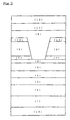
- numeral 1 represents a substrate
- numeral 2 represents a buffer layer
- numeral 3 represents a first conductive type clad layer
- numeral 4 represents an active layer
- numeral 5 represents a second conductive type first clad layer
- numeral 6 represents a second etching stop layer
- numeral 7 represents a first etching stop layer
- numeral 8 represents a second conductive type second clad layer
- numeral 9 represents a current block layer
- numeral 10 represents a cap layer
- numeral 11 represents a contact layer
- numeral 12 represents an electrode
- numeral 13 represents an electrode
- numeral 14 represents a passivation layer
- numerals 15, 16 represent coating layers.
- the compound semiconductor light emitting device according to the invention has a compound semiconductor layer containing a first conductive type clad layer, an active layer, and a second conductive type clad layer formed on a substrate, and a cavity structure is formed of two opposing facets of the compound semiconductor layer.
- the compound semiconductor light emitting device has features that surfaces of the first conductive type clad layer, the active layer, and the second conductive type clad layer forming the facet of the compound semiconductor are covered with a passivation layer, that at least one element constituting the facet of the compound semiconductor layer is not coupled to oxygen, and that a portion of the passivation layer adjacent to the facet of the compound semiconductor layer contains oxygen as a structural element.
- the structure of the invented compound semiconductor light emitting device is not specifically limited as far as the above conditions are satisfied. Accordingly, some layers other than the first conductive type clad layer, the active layer, and the second conductive type clad layer can be placed.
- the fabrication method for the invented compound semiconductor light emitting device is not specifically limited either. As a typical fabrication method, a method in which a semiconductor wafer is produced by forming respective layers on a substrate, in which cavity facets are formed on the produced semiconductor wafer, and in which the facets are covered with a passivation layer, can be exemplified.
- the semiconductor wafer used for fabrication of the compound semiconductor light emitting device according to the invention has an index guided structure and a structure that the second conductive type clad layer is divided into two layers, that a current injection region is formed by the second conductive type second clad layer and a current block layer, that a contact layer is formed to reduce the contact resistance to an electrode (Fig. 2).
- Fabrication methods for the basic epitaxial structures of various lasers, e.g., the above example as a typical device, can be exemplified by one described in Japanese Unexamined Patent Publication Heisei No.
- lasers 8-130,344 (Horie et al). These lasers are used as light sources in optical fiber amplifiers for optical communications, light sources for pick-up in large-capacity magneto-optical memory for data processing. Furthermore, these lasers are applicable to various uses by varying the layer structure, or materials to be used.
- Fig. 2 is schematic view of a structure of a groove type semiconductor laser as an example of the epitaxial structure in the present invention.
- a substrate (1) in consideration of the desired emission wavelength, lattice matching, strain intentionally introduced into the active layer, strain compensation in the active layer used for guide layers or the like, etc.
- single crystal substrates of InP, GaAs, GaN, InGaAs, Al 2 O 3 and the like can be used. Some dielectric substrates such as those made of Al 2 O 3 are also available in some cases.
- III-V group compound semiconductor light emitting devices containing As, P, and the like When as is contained as an element of the V group, it is most desirable to use a GaAs substrate. It is to be noted that in this specification the description of the group of the element is followed in a way of the IUPAC when it is described by Arabic numbers and followed in a way of a customary description when it is described by Roman numbers.
- Dielectric substrates such as those made of Al 2 O 3 , may be used for materials containing nitrogen as an element of the V group in III-V group semiconductor light emitting devices.
- off-angle substrates miss oriented substrates
- these off-angle substrates are employed widely.
- off-angle substrates are usually inclined by 0.5 to 2 degrees, those inclined around 10 degrees may be used in some material systems constituting a quantum well structure.
- the substrates may be subjected to, e.g., chemical etching, heat treatment, and the like in advance for the production of light emitting devices with the use of the crystal growth techniques such as MBE (Molecular Beam Epitaxy) or MOCDV (Metal Organic Chemical Vapor Deposition).
- crystal growth techniques such as MBE (Molecular Beam Epitaxy) or MOCDV (Metal Organic Chemical Vapor Deposition).
- the buffer layer (2) it is preferable to provide a buffer layer (2) to suppress the imperfectness in the substrate bulk crystals and facilitate the formation of epitaxial layers having the same crystal axis. It is preferable that the buffer layer (2) and the substrate (1) are made of the same compounds. When a GaAs substrate is used, for example, then GaAs is normally employed as the buffer layer. However, it also has been a practice to use a superlattice layer as the buffer layer. Namely, the buffer layer may be made of a different compound from the one of the substrate. When a dielectric substrate is used, on the other hand, it is not always needed that the buffer layer is made of the same compound, and a material different from the substrate can be appropriately selected as the buffer layer depending on the desired light emission wavelength and the whole structure of the device.
- the first conductive type clad layer (3) is usually made of a material having a lower refractive index than the average refractive index of the active layer (4). This material is appropriately specified depending on the substrate (1), buffer layer (2), active layer (4), etc. prepared for establishing the desired emission wavelength.
- GaAs is employed as both of the substrate and buffer layer (2), then AlGaAs based, InGaAs based, AlGalnP based, or InGaP based materials can be used for the first conductive type clad layer.
- the whole clad layer can be of a superlattice structure.
- the advantages of the invention can be recogni2ed notwithstanding the conductive type, the material, the structure, and the like of the active layer (4), but from the viewpoint of selecting the material, it is preferable that the active layer (4) is made of a material containing In and/or Ga, particularly, containing In.
- the most preferable material contains In and Ga. This is because the laser devices of the wavelength band realized by those materials when used for various applications are with great possibility demanded to have contradicting features of long lifetime and high output, both.
- the active layer (4) it is preferable to use AlGaAs based materials, InGaAs based materials, InGaP based materials, AlGalnP based materials, and the like. More specifically, In x Ga 1-x As (0 ⁇ x ⁇ 1) or (Al x Ga 1-x ) y In 1-y P (0 ⁇ x ⁇ 1, 0 ⁇ y ⁇ 1) is preferred. To realize a high output laser, it is preferable to have a quantum well structure. It is general that selection of those materials are determined depending on the desired emission wavelength.
- the active layer (4) can be a usual bulk active layer consisting of a single layer, quantum well structures such as single quantum well (SQW) structure, double quantum well (DQW) structure, multiple quantum well (MQW) structure, and the like can be employed depending on the purpose.
- the active layer of the quantum well structure is usually employed together with an optical guide layer.
- a barrier layer may be employed together, if needed.
- the separated confinement heterostructure (SCH) wherein optical guide layers are provided in both sides of the quantum well
- GRIN-SCH graded index-guided SCH
- a strained quantum well structure may be used to improve the laser property. It is also possible to select materials for the optical guide layers, to compensate the introduced strains in the whole active layers with employing opposite strains to the layers.
- the materials or the like of the optical guide layer may be selected to have strains reverse to the strains possessed by the quantum well layer to cancel strains as the active layer as a whole.
- the material of the optical guide layer may be appropriately selected from AlGaAs based material, InGaAs based material, InGaP based material, AIGalnP based material, AlInGaAs based material, InGaASP based material, GaAsP based material, and the like as to meet with the active layer.
- the optical guide layer can be a superlattice made in combination of the above materials. Moreover, the temperature characteristics can be improved by intentionally inserting a material having a large band gap between the quantum well and the optical guide layer.
- the second conductive type first and second clad layers (5), (8) are made of a material having a lower refractive index than the average refractive index of the active layer (4).
- This material is appropriately specified depending on the substrate (1), the buffer layer (2), the active layer (4), and the like.
- GaAs is employed as both of the substrate (1) and buffer layer (2), AlGaAs based material, InGaAs based material, InGaP based material, AlGalnP based material, AlInGaAs based material, InGaAsP based material, GaAsP based material, and the like can be used.
- Fig. 2 shows two types of etching stop layers (6), (7) and a cap layer (10). These layers, which are employed in a preferable embodiment of the present invention, are effective in precisely and easily forming the current injection region.
- the second etching stop layer (6) is made of, for example, an Al a Ga 1-a As (0 ⁇ a ⁇ 1) material, GaAs is preferably used ordinarily. This is because the second conductive type second clad layer (8) and the like can be grown with a good crystallinity particularly with the re-growth with the AlGaAs based material. It is usually preferable that the second etching stop layer (6) is 2 nm or thicker in thickness.
- the first etching stop layers (7) it is appropriate to use a layer represented by In b Ga 1-b P (0 ⁇ b ⁇ 1).
- b 0.5 is employed usually in a lattice-matched system.
- the first etching stop layer (7) is usually 5 nm or more, preferably 10 nm or more in thickness. When its thickness is less than 5 nm, etching may not be stopped due to undulation of the thickness or the like.
- a cap layer (10) is used as a protection layer for the current block layer (9) in the first growth and at the same time, to facilitate the growth of the second conductive type second clad layer (8). Before the device structure is completed, the cap layer is partly or completely removed.
- the current block layer (9) is required to literally block currents and not to flow any current substantially. Therefore, it is preferable that the layer has the same conductive type of the first conductive type clad layer (3) or undoped.
- a current block layer (9) is made of an AlGaAs based material the current block layer preferably has a refractive index lower than that of the second conductive type second clad layer (8) made of Al y Ga 1-y As (0 ⁇ y ⁇ 1). That is, where the current block layer is made of Al z Ga 1-z As (0 ⁇ z ⁇ 1), therefore, it is preferable that z is larger than y as the Al concentration.
- the second conductive type second clad layer (8) usually has a refractive index equal to or lower than that of the active layer (4).
- the second conductive type second clad layer (8) is usually the same as the first conductive type clad layer (3) and the second conductive type first clad layer (5).
- the second conductive type first clad layer (5), the second conductive type second clad layer (8), and the current block layer (9) can be all made of the same material basis of the same composition. In such a case, an effective refractive index difference is formed by the first etching stop layer (7).
- This contact layer (11) is usually made of a GaAs material.
- the carrier concentration in this layer is normally set higher than other layers.
- the thickness of the buffer layer (2) ranges from 0.1 to 3 ⁇ m; that of the first conductive type clad layer (3) ranges from 0.5 to 3 ⁇ m; that of the active layer (4) ranges from 0.0005 to 0.02 ⁇ m per layer in the case of the quantum well structure; that of the second conductive type first clad layer (5) ranges from 0.05 to 0.3 ⁇ m; that of the second conductive type second clad layer (8) ranges from 0. 5 to 3 ⁇ m; that of the cap layer (10) ranges from 0.05 to 0.5 ⁇ m; and that of the current block layer (9) ranges from 0.3 to 2 ⁇ m.
- the semiconductor light emitting device as shown in Fig. 2 is further provided with electrodes (12), (13).
- the electrode (12) is formed by an evaporation on the surface of the contact layer (11), for example, Ti / Pt / Au successively and then alloying them.
- the electrode (13) is formed on the surface of the substrate (1).
- the substrate (1) is successively deposited with AuGe/ Ni/ Au followed by alloying.
- the processed semiconductor wafer is formed with cavity facets.
- the cavity facet can be prepared by an ordinarily used method in the fabrication process for semiconductor light emitting devices, and there is no special limitation to the method.
- a method to make the wafer in a state of a so-called laser bar by forming facets by cleavage is widely used in the case of an edge-emission type laser, and the facets formed by cleavage are different according to the orientation of the substrate to be used.
- a device such as an edge-emission type laser is formed by using a substrate having a plane crystallographically equivalent to nominally (100) plane employed preferably, (110) plane or a plane crystallographically equivalent thereto serves as each of the plane for forming a cavity.
- the facets do not always meet at right angles with the direction of the cavity according to the relation between the inclination direction and the direction of the cavity.
- each of the facets is also inclined by two degrees.
- the cavity may be created during crystal growth likewise in the case of vertical cavity surface emitting lasers.
- troublesome cleavage step in vacuum is not always needed.
- Cleavage can be done under atmospheric pressure or in a nitrogen atmosphere. This is because the process such as plasma irradiation or the like done after cleavage can stably, reproductively suppress the surface state densities occurring on extrinsic causes. Therefore, the compound semiconductor light emitting device according to the invention can be manufactured in a simpler method.
- the plasma irradiation for stably, reproductively suppressing the surface state densities occurring on extrinsic causes is made to, at least, the first conductive type clad layer (3), the active layer (4), and the second conductive type clad layers (5), (8), which are exposed at the facet.
- the plasma can also be irradiated at that time to the substrate (1), the buffer layer (2), the first etching stop layer (7), the second etching stop layer (6), the current block layer (9), the cap layer (10), the contact layer (11), and the like which are exposed at the facet.
- plasma irradiation is preferably made to the entire facet or facets.
- a method for irradiating charged particles of a low energy around 25 to 300 eV, namely ions, electrons, and plasma as combination of those, preferably 18 groups or hydrogen plasma as a plasma source can be exemplified.
- 18 groups plasma sources helium or argon plasma, krypton plasma, xenon plasma can be exemplified specifically.
- Radiation of those to the facets removes oxides having relatively large vapor pressure (e.g., As-O, etc.) such as the V group or VI group among oxides of elements constituting the facets.
- the plasma irradiation is made in vacuum such as 10 -3 Torr or less, preferably 10 -4 Torr or less, most preferably 10 -5 Torr or less.
- plasma irradiation to the passivation layer formed on the facets is effective in contribution to suppress stably, reproducibly surface state densities occurring due to extrinsic causes.
- As-O or Ga-O particularly, As-O can be effectively removed by irradiating argon plasma or hydrogen plasma of low energies around 25 to 300 eV. Particularly, the irradiation of low energy argon plasma is remarkable. This method is superior, in comparison with ion implantations of impurities, because of very low processing energy as to make processing to the facets subjecting to lower damages.
- the compound semiconductor light emitting device it is preferable, by utilizing above methods, that at least one element constituting the facet of the compound semiconductor layer is not coupled to oxygen and that a portion of the passivation layer adjacent to the facet of the compound semiconductor layer contains oxygen as a structural element.
- an XPS X-ray photo-electron spectroscopy
- This method is very advantageous in analyzing the chemical binding of each element.
- the chemical binding of each element constituting a sample can be confirmed by exposing an X-ray condensed to a size of about 100 ⁇ m x 100 ⁇ m to the sample and spectroscopically analyzing the energy of photoelectrons generated resultantly.
- lasers are generally coated with a dielectric material optionally combined with a semiconductor at the facets, and therefore, prior to the above-mentioned XPS analysis, it is a practice to reduce the thickness of the coating film so as to have an appropriate thickness for the analysis by various etching techniques.
- the facets of the semiconductor laser can be analyzed without going through the above etching procedure and the like.
- the passivation layer is formed on the cavity facet thus formed.
- the phrase "passivation layer” means, in this specification, a layer formed on a facet of a compound semiconductor light emitting device for preventing chemical reactions with elements such as oxygen or the like which tend to form nonradiative recombination centers when coupled to elements constituting the facet.
- the passivation layer has a function, when oxygen or the like exists at the facet, to separate at least a part of the oxygen coupled to the elements constituting the semiconductor facet by oxidizing the passivation layer itself.
- a layer that comes to contain some oxide in a part by oxidizing the layer itself is also referred to as a "passivation layer" collectively.
- the passivation layer is formed as to cover at least a first conductive type clad layer, an active layer, and a second conductive type clad layer, which constitute the facet, but normally, formed as to cover the entire facet.
- the passivation layer in this invention is formed, after plasma is irradiated to the facets in vacuum, successively in vacuum, namely, in vacuum around 10 -3 Torr or less, preferably around 10 -6 Torr or less, most preferably, in high level vacuum of 10 -7 Torr or less.
- the passivation layer preferably contains an element having a greater absolute value of enthalpy (eV/metal atom) of formation of an oxide than an absolute value of enthalpy of formation of an oxide of at least one element constituting a semiconductor facet. Particularly, it is preferable that the passivation layer contains an element having a greater absolute value of enthalpy (eV/metal atom) of formation of an oxide than an absolute value of enthalpy of formation of an oxide of any element constituting a semiconductor facet.
- AlGaAs based material, InGaAs based material, InGaP based material, AIGalnP based material, AlInGaAs based material, InGaAsP based material, GaAsP based material, and the like are mainly used.
- elements of the group 2 can be used.
- the enthalpy of formation of Ga 2 O 3 is -5.64 eV/metal atom
- the enthalpy of formation of In 2 O 3 is -4.80 eV/metal atom.
- the enthalpy of formation of MgO is -6.24 eV/metal atom.
- the element suitably used for the passivation layer in this invention has a great absolute value of enthalpy of formation of an oxide.
- the passivation layer preferably includes one or more elements selected from a group of Si, Ge, S, Se, and Al, and more preferably includes Si.
- the enthalpy of formation of SiO 2 is -9.44 eV/metal atom, and it is the absolute value greater than an absolute value of enthalpy of formation of an oxide of any element constituting a semiconductor facet. Therefore, the passivation layer containing these elements is useful to various semiconductor materials. Particularly, such a passivation layer is very effective and useful for semiconductor materials excluding Al.
- the crystallographic structure and features of elements attached as the passivation layer (14) to the semiconductor facet may vary depending on the fabrication method, but any of single crystal, polycrystal, and amorphous can be found advantageous. Particularly, the layer formed at a low deposition rate in a high level vacuum is effective and very preferable.
- Si shows a refractive index (n + ik) to rays of emission wavelength of about 2 ⁇ m or shorter, wherein n means the real part of the refractive index, k is an extinction coefficient and n is about 3.5.
- the thickness Tp (nm) of the passivation layer (14) is thicker than 0.2 nm.
- an extremely thick passivation layer (14) of, for example, 100 nm is not suitable in some cases.
- the lower limit of the preferable thickness of the passivation layer (14) is specified by the factors for the existence of the passivation layer by itself as a film, while the upper limit thereof is determined from the balance to the effects of light absorption where light emitted from the active layer is absorbed by a part of the passivation layer.
- the passivation layer is deposited on the facet, namely, consideration should be made on the factor of coating the whole facets with the passivation layer and the effect of an increase in the temperature at the facets due to the absorption of emitted light.
- the passivation layer must be so thin as to reach at the facet the energy adequately inducing reducing reactions at the semiconductor facets.
- a preferable thickness range of the passivation layer is confirmed as represented by the following formula: 0.2 (nm) ⁇ Tp (nm) ⁇ ⁇ /8n (nm) where n means the real part of the average refractive index of the entire passivation layer at emission wavelength ⁇ .
- the above formula is no more than a desirable range, and the improved advantages are confirmed when the passivation layer has a thickness equal to and less than 0.2 nm.
- Oxidizing reaction is promoted at a portion of the passivation layer by oxygen derived from the semiconductor facet by plasma irradiation or heat irradiation for separating oxygen remaining on the facet or plasma irradiation implemented together when a coating material is supplied after formation of the passivation layer. It is preferable at that time for the passivation layer to have a thickness such that all the structural elements of the passivation layer are not oxidized. This is because if all the passivation layer is oxidized, the oxygen taken temporarily in the passivation layer may cause oxidation of the facet again during laser operation for a long time.
- all the elements constituting the semiconductor facet have no coupling to oxygen, but if all the passivation layer is oxidized, such a coupling of the elements constituting the semiconductor facet to oxygen may not be eliminated completely. Those situations are not favorable because those situations would reduce advantages in improved lifetime.
- coating layers (15), (16) made of a dielectric material or a combination of a dielectric material and a semiconductor on the passivation layer (14) formed on the exposed semiconductor facets (see, Fig. 1).
- plasma irradiation to the facets and formations of the passivation layer (14) and the coating layers (15), (16) are preferably performed successively under a negative pressure, more preferably, in vacuum.
- the coating layers are formed mainly for two purposes, to raise an emission efficiency from the semiconductor laser, and to further protect the facets.
- asymmetric coating in which a coating layer having a low reflectance with respect to the emission wavelength on the front facet and coating layers having a high reflectance with respect to the emission wavelength on the rear facet.
- Various materials are applicable to the coating layers (15), (16).
- the coating layer having a low reflectance use is made of AlOx, TiOx, SiOx, and the like, while the coating layers having a high reflectance are made of an AlOx/Si multilayered film, a TiOx/SiOx multilayered film, and the like.
- the thickness of each layer is controlled so as to give the desired reflectance. It is general to control the thickness of AlOx, TiOx, SiOx, and the like for constituting the coating layer having a low reflectance to be around ⁇ /4n where while n denotes the real part of the refractive index at the emission wavelength ⁇ . Also, for the coating layer having a high reflectance, it is general to adjust the respective materials constituting the layers to be around ⁇ /4n.
- IAD ion assisted deposition
- the plasma energy simultaneously irradiated at the formation of the coating films promotes the reactions described below, thereby making at least a part of the remaining oxides at the semiconductor facets changed as not to be in a form of an oxide where such oxides are remaining at the semiconductor facet. That is, the plasma irradiation promotes reactions that the structural elements existing in the passivation layer, particularly adjacent to the semiconductor facets, come to couple with oxygen remaining at the semiconductor facets. Consequently, it is possible to reduce the couplings between the elements constituting the semiconductor facets and oxygen down to a very low level or eliminate the couplings completely.
- This plasma irradiation is therefore an effective means to suppress the surface state densities as described above occurring due to extrinsic causes. It is to be noted that it is most preferable that the plasma irradiation is made simultaneously at the formation of the coating films, but it can be made before or after the formation of the coating films.
- an absolute value of enthalpy of formation between at least one element constituting the passivation layer and oxygen must be greater than an absolute value of enthalpy of formation between at least one element constituting a facet of the compound semiconductor layer and oxygen.
- the energies of supplied plasma or heats or the like are also required having an adequate amount to induce these reactions. Those energies are desirably selected within a range not to give excessive damages to the semiconductor facets.
- Si of the passivation layer facing the semiconductor facets comes to partly have a form of SiOx as a result of promoted couplings to oxygen derived from Ga-O. Therefore, the gallium constituting a part of the semiconductor facets is not in a form of the oxide, but in coupling to metal gallium or other elements constituting the semiconductor facets, forms, e.g., Ga-As. Consequently, the nonradiative recombination centers existing at the semiconductor facets derived from the Ga-O couplings are largely reduced, and therefore, the method can contribute to provide a desirable semiconductor light emitting devices having a high output and a long lifetime.
- another reaction may occur on a side of the coating film of the passivation layer as separately from the reactions on the semiconductor facets by such as elements partly constituting the coating films or nitrogen plasma fed in a form of plasma during film formation. That is, where the coating film is an oxide, the passivation layer may be oxidized by the film. Where the coating film is a nitride, nitriding reactions may be promoted.
- the passivation layer may be formed with the oxide at a portion adjacent to the compound semiconductor layer facets, and other portions may remain the structural elements of the passivation layer formed initially.
- the passivation layer may have a portion adjacent to the facet of the compound semiconductor layer made of an oxide, and an intermediate portion made of the structural elements or compound, as it is, of the passivation layer formed initially, and a portion adjacent to the coating layer made of the oxide, the nitride, the sulfide, or the like.
- the thickness of each layer is depending on the thickness of the passivation layer formed initially.
- an oxide layer or nitride layer of about 1 to 10 Angstroms on the side of the semiconductor facet and on the side of the coating film is produced, and the passivation layer not modified of several to several tens Angstroms remains at the center.
- a laser device of the groove type shown in Fig.2 was formed as following below procedures.
- SQW single quantum well
- a silicon nitride mask was formed on regions except the current injection region of the topmost layer.
- the silicon nitride mask had an opening width of 1.5 ⁇ m.
- Etching was performed by using the first etching stop layer (7) as an etching stop layer at 25 °C for 30 seconds so as to eliminate the cap layer (10) and the current block layer (9) in the current injection region. This etching was carried out with the use of a mixture of sulfuric acid (98 wt%), hydrogen peroxide (30 % aqueous solution) and water in a ratio of 1:1:5 by volume as an etching material or an etchant.
- the silicon nitride layer was removed in dipping a mixing solution mixing HF (49 %) and NH 4 F (40 %) at a rate of 1: 6 for 2 minutes and 30 seconds. Subsequently, the first etching stop layer in the current injection region was eliminated by etching at 25°C for 2 minutes with the use of the second etching stop layer as an etching stop layer.
- This etchant was a mixture of hydrochloric acid (35 wt %) and water at a ratio of 2: 1.
- a p-Al 0.35 Ga 0.65 As layer having a carrier concentration of 1 x 10 18 cm -3 was grown as the second conductive type second clad layer (8) by MOCVD method to obtain a thickness of 1.5 ⁇ m in buried part (i.e., the current injection region).
- a p-GaAs layer having a thickness of 3.5 ⁇ m and a carrier concentration of 1 x 10 19 cm -3 was grown as a contact layer (11) to maintain good electrical contact with the electrode.
- the width W of the current injection region (the width of the second conductive type second clad layer at the interface with the second etching stop layer) was 2.2 ⁇ m.
- this wafer was cleaved into laser bars of 700 ⁇ m in cavity length to expose the (100) plane, and the laser bars were thereby put in a vacuum chamber equipped with a plasma generator. Then, in the vacuum chamber of 3 x 10 -5 Torr, Ar plasma was irradiated to the facet (cleaved surface) at 60 eV in average energy and 150 ⁇ A/cm 2 in current density for one minute. Successively, in vacuum at 2 ⁇ 10 -3 Torr or below, amorphous Si was deposited in a thickness of 2 nm on the facets by the ordinary electron beam evaporation method, thereby forming a silicon passivation layer (14).
- AlO x film of 165 nm in thickness was successively formed so as to make the reflectance of the front facet 2.5 % at an emission wavelength of 980 nm, thereby forming a coating layer (15).
- Ar plasma having the average energy of 120 eV and a current density of 200 ⁇ A/cm 2 was applied in a vacuum of 4 ⁇ 10 -5 Torr to the facet at the same time as feeding of sources of the AlO x . It is confirmed that the real part of the refractive index of the amorphous Si at 980 nm was about 3.4.
- the laser bars were once taken out from the vacuum chamber to be treated on a side of the rear facet.
- the rear facet was treated in the same manner as those employed for the front facet, to perform Ar plasma irradiation and to form a silicon passivation layer (14), and successively, the coating layers (16) were formed so as to consist of four films, namely, AlO x layer having a thickness of 170nm, an amorphous Si of 60nm, AlO x of 170 nm, and an amorphous Si of 60nm, thereby forming the rear facet with the reflectance of 92%.
- the AlO x films were formed by the IAD method in the same manner as those employed for the front facet and the amorphous Si was formed by the electron beam evaporation method in the same manner as those employed for the front facet.
- An XPS measurement was carried out to analyze the front facet of a single sample of an obtained compound semiconductor light emitting device.
- the thickness of the AlOx at the front facet is reduced to about 20 Angstroms by a wet etching, and then, the measurement was carried out.
- the state of the semiconductor laser facet was observed with a photoelectron detection angle of 75°. Neither Ga-O nor As-O is detected though ordinarily existing on (110) plane exposed to air one time.
- the state of the amorphous Si was searched. As a result, although the film was produced in a good vacuum, it was confirmed that the amorphous Si had SiOx on the interface side to the semiconductor. This is that the oxygen of the oxide remaining at the facet of the compound semiconductor even after the initial plasma irradiation was coupled to Si formed in a film as the passivation layer by the energy of the plasma irradiation during the coating. It is to be noted that the enthalpy of formation of Ga 2 O 3 is -5.64 eV/metal atom, and the enthalpy of formation of SiO 2 is -9.44 eV/metal atom.
- the boundary between the amorphous Si produced as the passivation layer and the Alox coating layer was partly made into SiOx by oxygen from the Alox. That is, the layer of the amorphous Si produced as the passivation layer was confirmed as having a structure of SiOx/Si/SiOx from the side of the semiconductor facet.
- the thicknesses of the respective layers were about 6 Angstroms/ 6 Angstroms/ 8 Angstroms.
- Compound semiconductor light emitting devices were produced in substantially the same manner as Example 1 except some modified points that H 2 plasma of the average energy of 120 eV and a current density of 150 ⁇ A/cm 2 was irradiated for five minutes to the front and rear facets.
- An XPS measurement was carried out to analyze the front facet of a single sample of an obtained compound semiconductor light emitting device.
- the thickness of the AlOx at the front facet is reduced to about 20 Angstroms by a wet etching, and then, the measurement was carried out.
- the state of the semiconductor laser facet was observed with a photoelectron detection angle of 75°. Neither Ga-O nor As-O is detected though ordinarily existing on (110) plane exposed to air one time.
- the state of the amorphous Si was searched. As a result, although the film was produced in a good vacuum, it was confirmed that the amorphous Si had SiOx on the interface side to the semiconductor. This is that the oxygen of the oxide remaining at the facet of the compound semiconductor even after the initial plasma irradiation was coupled to Si formed in a film as the passivation layer by the energy of the plasma irradiation during the coating.
- the boundary between the amorphous Si produced as the passivation layer and the AlO x coating layer was partly made into SiOx by oxygen from the AlOx. That is, the layer of the amorphous Si produced as the passivation layer was confirmed as having a structure of SiOx/Si/siOx from the side of the semiconductor facet. The thicknesses of the respective layers were about 5 Angstroms/ 8 Angstroms/ 7 Angstroms.
- Compound semiconductor light emitting devices were produced in substantially the same manner as Example 1 except some modified points that after a passivation layer was formed on the front and rear facets, Ar plasma of the average energy of 110 eV and a current density of 200 ⁇ A/cm 2 was radiated for 30 seconds in vacuum of 4 x 10 -5 Torr to the passivation layer without feeding any source for the coating layer, and successively AlO x was formed by an ordinary electron beam evaporation.
- An XPS measurement was carried out to analyze the front facet of a single sample of an obtained compound semiconductor light emitting device.
- the thickness of the AlOx at the front facet is reduced to about 20 Angstroms by a wet etching, and then, the measurement was carried out.
- the state of the semiconductor laser facet was observed with a photoelectron detection angle of 75°. Neither Ga-O nor As-O is detected though ordinarily existing on (110) plane exposed to air one time.
- the state of the amorphous Si was searched. As a result, although the film was produced in a good vacuum, it was confirmed that the amorphous Si had SiOx on the interface side to the semiconductor. This is that the oxygen of the oxide remaining at the facet of the compound semiconductor even after the initial plasma irradiation was coupled to Si formed in a film as the passivation layer by the energy of the plasma irradiation during the coating.
- the boundary between the amorphous Si produced as the passivation layer and the AlOx coating layer was partly made into SiOx by oxygen from the AlOx. That is, the layer of the amorphous Si produced as the passivation layer was confirmed as having a structure of SiOx/Si/SiOx from the side of the semiconductor facet.
- the thicknesses of the respective layers were about 7 Angstroms/ 5 Angstroms/ 8 Angstroms.
- Compound semiconductor light emitting devices were produced in substantially the same manner as Example 1 except some modified points that after a passivation layer was formed on the front and rear facets, Ar plasma of the average energy of 110 eV and a current density of 200 ⁇ A/cm 2 was radiated in vacuum of 4 x 10 -5 Torr to the facets on which the silicon passivation layer was formed, and successively an amorphous Si serving as the passivation layer was evaporated by about 10 Angstroms in a vacuum of 2 x 10 -7 Torr or less using an ordinary electron beam evaporation, and another Ar plasma of the average energy of 120 eV and a current density of 200 ⁇ A/cm 2 was radiated in vacuum of 4 x 10 -5 Torr simultaneously with supply of AlOx to the facets in use of the IAD method.
- An XPS measurement was carried out to analyze the front facet of a single sample of an obtained compound semiconductor light emitting device.
- the thickness of the AlOx at the front facet is reduced to about 20 Angstroms by a wet etching, and then, the measurement was carried out.
- the state of the semiconductor laser facet was observed with a photoelectron detection angle of 75°. Neither Ga-O nor As-O is detected though ordinarily existing on (110) plane exposed to air one time.
- the state of the amorphous Si was searched. As a result, although the film was produced in a good vacuum, it was confirmed that the amorphous Si had SiOx on the interface side to the semiconductor. This is that the oxygen of the oxide remaining at the facets of the compound semiconductor even after the initial plasma irradiation was coupled to Si formed in a film as the passivation layer by the energy of the plasma irradiation during the coating.
- the boundary between the amorphous Si produced as the passivation layer and the AlOx coating layer was partly made into SiOx by oxygen from the AlOx. That is, the layer of the amorphous Si produced as the passivation layer was confirmed as having a structure of SiOx/Si/SiOx from the side of the semiconductor facet.
- the thicknesses of the respective layers were about 7 Angstroms/ 15 Angstroms/ 8 Angstroms.
- Compound semiconductor light emitting devices were produced in substantially the same manner as Example 1 except some modified points that after a passivation layer was formed, Ar plasma of the average energy of 110 eV and a current density of 200 ⁇ A/cm 2 was radiated in vacuum of 4 x 10 -5 Torr to the facets on which the silicon passivation layer was formed, and successively an amorphous Si serving as the passivation layer was evaporated by about 10 Angstroms in a vacuum of 2 x 10 -7 Torr or less using an ordinary electron beam evaporation, and subsequently, N 2 plasma of the average energy of 130 eV and a current density of 400 ⁇ A/cm 2 was radiated in vacuum of 7 x 10 -5 Torr simultaneously with supply of Si to the facets in use of the IAD method to produce a SiN to render the reflectance of the front facet 7% and in substantially the same manner for the rear facet, in use of the IAD method to produce a SiN instead of the Alox to render the reflectance of the rear
- An XPS measurement was carried out to analyze the front facet of a single sample of an obtained compound semiconductor light emitting device.
- the thickness of the AlOx at the front facet is reduced to about 20 Angstroms by a wet etching, and then, the measurement was carried out.
- the state of the semiconductor laser facet was observed with a photoelectron detection angle of 75°. Neither Ga-O nor As-O is detected though ordinarily existing on (110) plane exposed to air one time.
- the state of the amorphous Si was searched. As a result, although the film was produced in a good vacuum, it was confirmed that the amorphous Si had SiOx on the interface side to the semiconductor. This is that the oxygen of the oxide remaining at the facet of the compound semiconductor even after the initial plasma irradiation was coupled to Si formed in a film as the passivation layer by the energy of the plasma irradiation during the coating.
- the boundary between the amorphous Si produced as the passivation layer and the SiN coating layer was partly made into SiNx by oxygen from the coating layer. That is, the layer of the amorphous Si produced as the passivation layer was confirmed as having a structure of SiOx/Si/SiNx from the side of the semiconductor facet.
- the thicknesses of the respective layers were about 7 Angstroms/ 12 Angstroms/ 11 Angstroms.
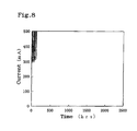
- Compound semiconductor light emitting devices were prepared in substantially the same manner as Example 1 except some modified points that no formation of the Si passivation layer and no Ar plasma irradiation preceding to this was made on both of the front and rear facets, and that the coating layers are formed not by the IAD method but by an ordinary electron beam evaporation which was made to the entire layers.
- the threshold current was 23 mA at 25 °C, and kink was observed at 350 mA, 250mW.
- ten devices, all were subject to sudden failure as shown in Fig. 8 by or before passing 100 hours.
- the XPS analysis was carried out in substantially the same manner as Example 1, it was confirmed that Ga-O existed at the facets.
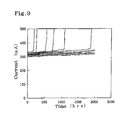
- Compound semiconductor light emitting devices were prepared in substantially the same manner as Example 1 except some modified points that no formation of the Si passivation layer was made on both of the front and rear facets.
- the threshold current was 23 mA at 25 °C, and kink was observed at 350 mA, 250mW.
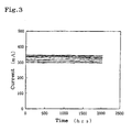
- the aging test 200 mW, 50 °C
- six devices among eleven device were subject to sudden failure as shown in Fig. 9 when passing 2,000 hours.
- the degradation rate is greater than that of Example 1.
- Compound semiconductor light emitting devices were prepared in substantially the same manner as Example 1 except some modified points that no Ar plasma irradiation preceding to formation of the Si passivation layer was made on both of the front and rear facets.
- the threshold current was 23 mA at 25 °C, and kink was observed 350 mA, 250mW.
- ten devices, all were subject to sudden failure as shown in Fig. 10 when passing 250 hours.
- the XPS analysis was carried out in substantially the same manner as Example 1, it was confirmed that Ga-O and small amount of As-O existed at the facets.
- Compound semiconductor light emitting devices were prepared in substantially the same manner as Example 2 except some modified points that formation of the Si passivation layer and Ar plasma irradiation preceding to the formation were not made on both of the front and rear facets.
- the compound semiconductor light emitting device according to the invention As describe above, with the compound semiconductor light emitting device according to the invention, the surface state densities at the facets can be stably suppressed for a long time, and the laser devices have a high output, a long lifetime, and a high performance.
- the compound semiconductor light emitting devices according to the invention have practical advantages in reducing the degradation at the facets and fabrication with a simpler method allowing cleavage in air. Therefore, the compound semiconductor light emitting devices according to the invention provide significant industrial interests and have very wide applicable fields.
- the invention also consists in the methods of manufacture of light emitting devices herein described.
Landscapes
- Semiconductor Lasers (AREA)
- Led Devices (AREA)
Applications Claiming Priority (2)
| Application Number | Priority Date | Filing Date | Title |
|---|---|---|---|
| JP34479898 | 1998-12-04 | ||
| JP34479898A JP3814432B2 (ja) | 1998-12-04 | 1998-12-04 | 化合物半導体発光素子 |
Publications (2)
| Publication Number | Publication Date |
|---|---|
| EP1006629A2 true EP1006629A2 (fr) | 2000-06-07 |
| EP1006629A3 EP1006629A3 (fr) | 2003-07-30 |
Family
ID=18372079
Family Applications (1)
| Application Number | Title | Priority Date | Filing Date |
|---|---|---|---|
| EP99309728A Withdrawn EP1006629A3 (fr) | 1998-12-04 | 1999-12-03 | Dispositif émetteur de lumière à semi-conducteur composé |
Country Status (3)
| Country | Link |
|---|---|
| US (1) | US6677618B1 (fr) |
| EP (1) | EP1006629A3 (fr) |
| JP (1) | JP3814432B2 (fr) |
Cited By (4)
| Publication number | Priority date | Publication date | Assignee | Title |
|---|---|---|---|---|
| WO2003096498A3 (fr) * | 2002-05-13 | 2004-07-29 | Forschungsverbund Berlin Ev | Procede de passivation des surfaces reflectrices de composants a semiconducteurs optiques |
| DE102007059538A1 (de) * | 2007-12-11 | 2009-06-18 | Lumics Gmbh | Passivierung einer Resonator-Endfläche eines Halbleiter-Lasers mit einem Halbleiter-Übergitter |
| EP1866955A4 (fr) * | 2005-03-25 | 2011-02-02 | Trumpf Photonics Inc | Passivation de facettes de laser |
| WO2023152023A1 (fr) * | 2022-02-10 | 2023-08-17 | Ams-Osram International Gmbh | Dispositif à semi-conducteur optoélectronique et procédé de fabrication |
Families Citing this family (13)
| Publication number | Priority date | Publication date | Assignee | Title |
|---|---|---|---|---|
| WO2001022545A1 (fr) * | 1999-09-22 | 2001-03-29 | Mitsubishi Chemical Corporation | Element lumineux et module d'element lumineux |
| US7173953B2 (en) * | 2001-11-06 | 2007-02-06 | Bookham Technology Plc | Anti-reflection coatings for semiconductor lasers |
| JP4236840B2 (ja) * | 2001-12-25 | 2009-03-11 | 富士フイルム株式会社 | 半導体レーザ素子 |
| US20040119080A1 (en) * | 2002-08-12 | 2004-06-24 | Hashimoto Jun-Ichi | Semiconductor optical device |
| JP2004119817A (ja) * | 2002-09-27 | 2004-04-15 | Sharp Corp | 半導体レーザ素子およびその製造方法 |
| JP2005072488A (ja) * | 2003-08-27 | 2005-03-17 | Mitsubishi Electric Corp | 半導体レーザ装置 |
| JP2007109737A (ja) * | 2005-10-11 | 2007-04-26 | Toshiba Corp | 窒化物半導体レーザ装置及びその製造方法 |
| DE102007062050B4 (de) * | 2007-09-28 | 2019-06-27 | Osram Opto Semiconductors Gmbh | Halbleiterlaser und Verfahren zum Herstellen des Halbleiterlasers |
| FR2930680B1 (fr) * | 2008-04-23 | 2010-08-27 | Commissariat Energie Atomique | Procede de fabrication d'une cellule photovoltaique a base de silicium en couches minces. |
| US8198112B2 (en) | 2010-04-14 | 2012-06-12 | Corning Incorporated | Laser diodes comprising QWI output window and waveguide areas and methods of manufacture |
| EP2377607B1 (fr) * | 2010-04-19 | 2018-05-30 | Corning Incorporated | Raccords fluides pour modules de microréacteur |
| US8369371B1 (en) * | 2010-10-22 | 2013-02-05 | Science Research Laboratory, Inc. | Passivated semiconductor surfaces |
| DE102017112610A1 (de) | 2017-06-08 | 2018-12-13 | Osram Opto Semiconductors Gmbh | Kantenemittierender Halbleiterlaser und Betriebsverfahren für einen solchen Halbleiterlaser |
Family Cites Families (16)
| Publication number | Priority date | Publication date | Assignee | Title |
|---|---|---|---|---|
| US4656638A (en) * | 1983-02-14 | 1987-04-07 | Xerox Corporation | Passivation for surfaces and interfaces of semiconductor laser facets or the like |
| US4563368A (en) | 1983-02-14 | 1986-01-07 | Xerox Corporation | Passivation for surfaces and interfaces of semiconductor laser facets or the like |
| JPH0245992A (ja) | 1988-08-06 | 1990-02-15 | Mitsubishi Electric Corp | 半導体レーザ装置 |
| US5144634A (en) | 1989-09-07 | 1992-09-01 | International Business Machines Corporation | Method for mirror passivation of semiconductor laser diodes |
| EP0416190B1 (fr) | 1989-09-07 | 1994-06-01 | International Business Machines Corporation | Méthode de passivation des miroirs des diodes laser à semi-conducteur |
| JPH03131083A (ja) | 1989-10-17 | 1991-06-04 | Mitsubishi Electric Corp | 半導体レーザ装置の製造方法 |
| DE69006353T2 (de) | 1990-05-25 | 1994-06-23 | Ibm | Verfahren und Vorrichtung zum Spalten von Halbleiterplatten und Bekleiden der gespalteten Facetten. |
| JPH04336426A (ja) | 1991-05-14 | 1992-11-24 | Fujitsu Ltd | 半導体装置の製造方法 |
| US6022458A (en) | 1992-12-07 | 2000-02-08 | Canon Kabushiki Kaisha | Method of production of a semiconductor substrate |
| JPH06302906A (ja) | 1993-04-12 | 1994-10-28 | Mitsubishi Electric Corp | 半導体レーザ及びその製造方法 |
| JP3136385B2 (ja) | 1993-12-08 | 2001-02-19 | 株式会社日立製作所 | 耐熱耐酸化性高強度部材及びその製造方法 |
| US5440575A (en) * | 1994-04-06 | 1995-08-08 | At&T Corp. | Article comprising a semiconductor laser with stble facet coating |
| JP3689733B2 (ja) | 1994-07-04 | 2005-08-31 | 三菱化学株式会社 | 半導体素子の製造方法 |
| JP3101183B2 (ja) | 1995-07-28 | 2000-10-23 | 株式会社新潟鉄工所 | 温泉水の揚水装置及び揚水方法 |
| FR2742926B1 (fr) * | 1995-12-22 | 1998-02-06 | Alsthom Cge Alcatel | Procede et dispositif de preparation de faces de laser |
| JPH1084161A (ja) * | 1996-09-06 | 1998-03-31 | Sumitomo Electric Ind Ltd | 半導体レーザ及びその製造方法 |
-
1998
- 1998-12-04 JP JP34479898A patent/JP3814432B2/ja not_active Expired - Fee Related
-
1999
- 1999-12-03 EP EP99309728A patent/EP1006629A3/fr not_active Withdrawn
- 1999-12-03 US US09/453,279 patent/US6677618B1/en not_active Expired - Fee Related
Cited By (6)
| Publication number | Priority date | Publication date | Assignee | Title |
|---|---|---|---|---|
| WO2003096498A3 (fr) * | 2002-05-13 | 2004-07-29 | Forschungsverbund Berlin Ev | Procede de passivation des surfaces reflectrices de composants a semiconducteurs optiques |
| DE10221952B4 (de) * | 2002-05-13 | 2007-07-12 | Forschungsverbund Berlin E.V. | Verfahren zur Passivierung der Spiegelflächen von optischen Halbleiterbauelementen |
| EP1866955A4 (fr) * | 2005-03-25 | 2011-02-02 | Trumpf Photonics Inc | Passivation de facettes de laser |
| DE102007059538A1 (de) * | 2007-12-11 | 2009-06-18 | Lumics Gmbh | Passivierung einer Resonator-Endfläche eines Halbleiter-Lasers mit einem Halbleiter-Übergitter |
| DE102007059538B4 (de) * | 2007-12-11 | 2009-08-20 | Lumics Gmbh | Passivierung einer Resonator-Endfläche eines Halbleiter-Lasers mit einem Halbleiter-Übergitter |
| WO2023152023A1 (fr) * | 2022-02-10 | 2023-08-17 | Ams-Osram International Gmbh | Dispositif à semi-conducteur optoélectronique et procédé de fabrication |
Also Published As
| Publication number | Publication date |
|---|---|
| US6677618B1 (en) | 2004-01-13 |
| JP2000174378A (ja) | 2000-06-23 |
| JP3814432B2 (ja) | 2006-08-30 |
| EP1006629A3 (fr) | 2003-07-30 |
Similar Documents
| Publication | Publication Date | Title |
|---|---|---|
| US6744074B2 (en) | Compound semiconductor light emitting device and method of fabricating the same | |
| US6677618B1 (en) | Compound semiconductor light emitting device | |
| US6876002B2 (en) | Semiconductor laser device and method for manufacturing the same | |
| Horie et al. | Reliability improvement of 980-nm laser diodes with a new facet passivation process | |
| JP2000082863A (ja) | 半導体発光素子の製造方法 | |
| JP2001196694A (ja) | 半導体レーザ素子及びその製造方法 | |
| JP3797798B2 (ja) | 半導体発光素子の製造方法 | |
| JP3699851B2 (ja) | 半導体発光素子の製造方法 | |
| JP3699842B2 (ja) | 化合物半導体発光素子 | |
| JP3707947B2 (ja) | 半導体発光素子 | |
| JP3710627B2 (ja) | 化合物半導体発光素子 | |
| JPH05218593A (ja) | 半導体レーザの製造方法 | |
| JP2003008149A (ja) | 半導体レーザ装置 | |
| EP1109231A2 (fr) | Dispositif semi-conducteur émetteur de lumière et méthode de fabrication | |
| JP3699840B2 (ja) | 化合物半導体発光素子 | |
| JP2002124738A (ja) | 半導体光デバイス装置及びその製造方法 | |
| JP2001185809A (ja) | 半導体光デバイス装置及びその製造方法 | |
| US6670211B2 (en) | Semiconductor laser device | |
| JP3797797B2 (ja) | 半導体発光素子の製造方法 | |
| JP2990009B2 (ja) | 半導体レーザ及び半導体レーザの製造方法 | |
| JP2003198059A (ja) | 半導体レーザ素子およびその製造方法 | |
| JP3699841B2 (ja) | 化合物半導体発光素子 | |
| JP2003152282A (ja) | 半導体レーザ素子 | |
| JP3754822B2 (ja) | 化合物半導体発光素子 | |
| JPH10223978A (ja) | 半導体レーザおよびその製造方法 |
Legal Events
| Date | Code | Title | Description |
|---|---|---|---|
| PUAI | Public reference made under article 153(3) epc to a published international application that has entered the european phase |
Free format text: ORIGINAL CODE: 0009012 |
|
| AK | Designated contracting states |
Kind code of ref document: A2 Designated state(s): AT BE CH CY DE DK ES FI FR GB GR IE IT LI LU MC NL PT SE |
|
| AX | Request for extension of the european patent |
Free format text: AL;LT;LV;MK;RO;SI |
|
| PUAL | Search report despatched |
Free format text: ORIGINAL CODE: 0009013 |
|
| AK | Designated contracting states |
Designated state(s): AT BE CH CY DE DK ES FI FR GB GR IE IT LI LU MC NL PT SE |
|
| AX | Request for extension of the european patent |
Extension state: AL LT LV MK RO SI |
|
| RIC1 | Information provided on ipc code assigned before grant |
Ipc: 7H 01S 5/028 B Ipc: 7H 01L 33/00 B Ipc: 7H 01S 5/32 A |
|
| 17P | Request for examination filed |
Effective date: 20030908 |
|
| 17Q | First examination report despatched |
Effective date: 20040122 |
|
| AKX | Designation fees paid |
Designated state(s): FR GB IT |
|
| REG | Reference to a national code |
Ref country code: DE Ref legal event code: 8566 |
|
| RAP1 | Party data changed (applicant data changed or rights of an application transferred) |
Owner name: MITSUBISHI CHEMICAL CORPORATION |
|
| GRAC | Information related to communication of intention to grant a patent modified |
Free format text: ORIGINAL CODE: EPIDOSCIGR1 |
|
| GRAP | Despatch of communication of intention to grant a patent |
Free format text: ORIGINAL CODE: EPIDOSNIGR1 |
|
| RAP1 | Party data changed (applicant data changed or rights of an application transferred) |
Owner name: MITSUBISHI CHEMICAL CORPORATION |
|
| STAA | Information on the status of an ep patent application or granted ep patent |
Free format text: STATUS: THE APPLICATION IS DEEMED TO BE WITHDRAWN |
|
| 18D | Application deemed to be withdrawn |
Effective date: 20061219 |