EP1006648A2 - Aktive Kompensation eines kapazitiven Multiplizierers - Google Patents
Aktive Kompensation eines kapazitiven Multiplizierers Download PDFInfo
- Publication number
- EP1006648A2 EP1006648A2 EP99203275A EP99203275A EP1006648A2 EP 1006648 A2 EP1006648 A2 EP 1006648A2 EP 99203275 A EP99203275 A EP 99203275A EP 99203275 A EP99203275 A EP 99203275A EP 1006648 A2 EP1006648 A2 EP 1006648A2
- Authority
- EP
- European Patent Office
- Prior art keywords
- amplifier
- node
- fet
- stage
- current
- Prior art date
- Legal status (The legal status is an assumption and is not a legal conclusion. Google has not performed a legal analysis and makes no representation as to the accuracy of the status listed.)
- Granted
Links
Images

Classifications
-
- H—ELECTRICITY
- H03—ELECTRONIC CIRCUITRY
- H03F—AMPLIFIERS
- H03F3/00—Amplifiers with only discharge tubes or only semiconductor devices as amplifying elements
- H03F3/45—Differential amplifiers
- H03F3/45071—Differential amplifiers with semiconductor devices only
- H03F3/45076—Differential amplifiers with semiconductor devices only characterised by the way of implementation of the active amplifying circuit in the differential amplifier
- H03F3/45179—Differential amplifiers with semiconductor devices only characterised by the way of implementation of the active amplifying circuit in the differential amplifier using MOSFET transistors as the active amplifying circuit
- H03F3/45183—Long tailed pairs
-
- H—ELECTRICITY
- H03—ELECTRONIC CIRCUITRY
- H03F—AMPLIFIERS
- H03F1/00—Details of amplifiers with only discharge tubes, only semiconductor devices or only unspecified devices as amplifying elements
- H03F1/08—Modifications of amplifiers to reduce detrimental influences of internal impedances of amplifying elements
- H03F1/083—Modifications of amplifiers to reduce detrimental influences of internal impedances of amplifying elements in transistor amplifiers
- H03F1/086—Modifications of amplifiers to reduce detrimental influences of internal impedances of amplifying elements in transistor amplifiers with FET's
-
- H—ELECTRICITY
- H03—ELECTRONIC CIRCUITRY
- H03F—AMPLIFIERS
- H03F2200/00—Indexing scheme relating to amplifiers
- H03F2200/153—Feedback used to stabilise the amplifier
-
- H—ELECTRICITY
- H03—ELECTRONIC CIRCUITRY
- H03F—AMPLIFIERS
- H03F2203/00—Indexing scheme relating to amplifiers with only discharge tubes or only semiconductor devices as amplifying elements covered by H03F3/00
- H03F2203/45—Indexing scheme relating to differential amplifiers
- H03F2203/45118—At least one reactive element being added to at least one feedback circuit of a dif amp
-
- H—ELECTRICITY
- H03—ELECTRONIC CIRCUITRY
- H03F—AMPLIFIERS
- H03F2203/00—Indexing scheme relating to amplifiers with only discharge tubes or only semiconductor devices as amplifying elements covered by H03F3/00
- H03F2203/45—Indexing scheme relating to differential amplifiers
- H03F2203/45512—Indexing scheme relating to differential amplifiers the FBC comprising one or more capacitors, not being switched capacitors, and being coupled between the LC and the IC
Definitions
- This invention relates to frequency compensation of electronic circuits, and more particularly relates to circuits having compensating capacitors, such as Miller Effect capacitors.
- phase margin The stability performance of circuits having feedback is improved by providing compensation so as to increase phase margin.
- a well known technique for improving phase margin takes advantage of the Miller Effect, by adding a Miller-compensating capacitance in parallel with a gain stage, (e.g. the output stage of a two stage amplifier circuit).
- a gain stage e.g. the output stage of a two stage amplifier circuit.
- pole splitting Such a configuration results in the well-known and desirable phenomenon called pole splitting, which advantageously multiplies the effective capacitance of the physical capacitor employed in the circuit. See, for example, for background on compensation of amplifier circuits using Miller-compensating capacitance, Paul R. Gray and Robert G. Meyer, Analysis and Design of Analog Integrated Circuits, Third Ed., John Wiley & Sons, Inc., New York, 1993, Ch. 9, especially pp. 607-623.
- the present application discloses an improved compensated amplifier, for amplifying an input signal applied to an input node to provide an output signal at an amplifier output node.
- the compensated amplifier includes a first amplifier stage having an internal node functioning as an input thereto and having a first stage output node. Also included is a second amplifier stage coupled to the first amplifier stage, having the input node as an input thereto and providing the output signal at the amplifier output node.
- a capacitor is coupled between the output node and the internal node.
- the amplifier may be advantageously applied for the purpose of multiplying Miller-compensating capacitance, although it is not limited to that application.
- amplifier as used herein is not limited to any specific form of amplifier, such as an operational amplifier. Rather, the term is intended to refer to any circuit that provides an amplified form of an input signal applied thereto.
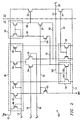
- FIG. 1 is a schematic diagram of a prior art differential amplifier 10 including a Miller-compensating capacitor C1 .
- a supply voltage V DD is provided between a supply rail 12 and a ground rail 13 .
- a sinking bias current i B is provided on an input line 14.
- a differential input is provided, with the positive going signal V p being provided on input line 16 and the negative going signal V n being provided on input line 18 .
- the amplifier 10 structure is two stage.
- the first stage 20 is a folded-cascode differential amplifier.
- the second stage 22 is a Miller-compensated PMOS device amplifier.
- the differential inputs on lines 16 and 18 are provided to the respective gates of a pair of PMOS devices 24, 26.
- the differential current generated through devices 24, 26, is reflected into NMOS devices 28, 30.
- the voltage on the drain of device 30 is sensed at the gate of output PMOS device 32 .
- Capacitor C1 and resistor R1 series connected between the drain and gate of device 32 , provide Miller compensation for amplifier 10.
- NMOS device 34 provides a quiescent bias current for output PMOS transistor 32 .
- PMOS device structure 38 is a multiple output current mirror.
- Device 40 is diode-connected and establishes a stable internal bias voltage, based on the input bias current i B on line 14. This stable bias current i B is thus mirrored by devices 42, 44, 46, and 48.
- the mirrored current in device 42 is converted into another stable bias voltage by NMOS device 50 at node 52, which biases the gates of devices 28, 30.
- the mirrored current in device 44 is also mirrored by NMOS current mirror 54 to force current generation via node 56 through device 28 and device 24.
- the mirrored current in device 48 is also mirrored by NMOS current mirror 58 to force current generation via node 60 through device 30 and device 26.
- the mirrored current in device 46 provides a stable bias current for devices 24 and 26.
- the current mirror 64 provides an ac path and a stable current supply, via lines 66 and 68 , to devices 28 and 30, respectively.
- the circuit 10 described above in Figure 1 is known, and provides generally acceptable performance.
- the use of a Miller-compensating capacitor results in a multiplication of the effective compensating capacitance, enhancing the desirable, and known, effect of pole splitting.
- the Miller-compensating capacitor C1 must also increase in value to maintain stability in the circuit 10. This can result in capacitor C1 occupying more physical space than is desired, or even than can be afforded.
- FIG 2 is a schematic diagram of a differential amplifier 100 including a Miller-compensating capacitor C2 in accordance with the principles disclosed by the present application. Similar to the circuit 10 of Figure 1 , the amplifier 100 structure is two stage, the first stage 20' being a folded-cascode differential amplifier, and the second stage 22' being a Miller-compensated PMOS device amplifier. Unlike the circuit 10 of Figure 1 , however, Miller-compensating capacitor C1 and resistor R1 are not provided.
- the circuit 100 of Figure 2 includes a novel capacitor arrangement consisting of capacitor C2 connected between the output node 36' and the common connection node 102 for the gates of the two NMOS devices-an NMOS device 104 diode-connected, and an NMOS device 106 ratioed by a factor of ten as compared with device 104, comprising current mirror 54'.
- capacitor C2 By connecting capacitor C2 in this way, the feedback current flowing through capacitor C2 is amplified, i.e. multiplied by, e.g., ten by current mirror 54' before reaching the high impedance node 68 .
- the resulting load capacitance seen by the high-impedance node 68 is then ten times greater than the Miller-multiplied version connected using prior art principles.
- the value ten for the multiplication factor described above is arbitrary, and is selected for example only.
- the gain, and thus the multiplication factor, is ultimately achieved in the circuit of Figure 2 by the effective current amplification by current mirror 54', and its limitation depends on the physical restrictions, or spread, of current mirror 54'.
- the mirror ratio of the current flowing through current mirror 54' i.e., the ratio of the widths of device 106 and device 104, and thus the ratio of the current flowing through device 106 as compared with device 104, is ten.
- Other ratios, and thus other capacitance multiplication factors are possible.
- the width of PMOS device 44 is reduced by the same ratio.
- PMOS device 48 and current mirror 58 are made to match PMOS device 44 and current mirror 54. Key is the amplification of the compensating capacitor's current.
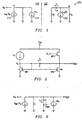
- FIG 3 shows an ac-equivalent model 200 of the amplifier circuit of Figure 2 .
- the model 200 has two stages, a first stage 210 and a second stage 220.
- second stage 220 a voltage V x is seen at the input of Miller-compensating capacitance C m and an ac current I x flows through internal resistance R i .
- the current I x is reflected back through block 214, multiplied by ten, to the input circuit 210.
- Equation 4 there is no right-hand plane zero.
- a Left Hand Plane (LHP) zero is inserted.
- This LHP zero can be used to optimize the compensation of the loop in Figure 2 created by the connection of capacitor C2 between the output node 36' in the second stage 22' and the common gate connection of devices 104 and 106 in the first stage 20', which is controlled by the transconductance of device 104.
- the dominant pole for the circuit 100 of Figure 2 is defined by the high impedance node 68 and ten times the gain of the second stage 22' times the Miller-compensating capacitance C2.
- the LHP zero can be designed to lie approximately where the pole of output node 36' lies. As a result, the pole is cancelled and phase margin is consequently increased.
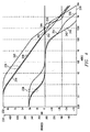
- Figure 4 is a graph showing Bode plots of the behavior of different circuits like the circuit shown in Figure 1 and the circuit shown in Figure 2. This figure helps in understanding the principles presented in the immediately preceding paragraph.
- Two different sets of curves 236, 238, are shown in Figure 4.
- a first axis 232 representing the gain of the respective circuit and divided into units of decibels ("DB")
- DB decibels
- a second axis 234 representing the relative phase of the output signal as compared with the phase of the input signal, and divided into units of degrees.
- the first set of curves 236 is plotted against the gain axis 232, while the second set of curves 238 is plotted against the phase shift axis 234.
- a zero relative phase compared with the input is 0°, which is the same as 360°.
- the curves 238 all tend to drop, showing a decrease in phase from 360° as frequency increases.
- the curves 236 all tend to drop, showing a decrease in gain as frequency increases.
- a first curve 240 is a plot of the gain of a representative circuit constructed like that of Figure 1 , against frequency, in which the compensating-capacitance C1 is 2 pF.
- a third curve 248 is a plot of the gain of a representative circuit constructed like that of Figure 1, against frequency, in which the compensating-capacitance C1 is 20 pF.
- a fourth curve 250 is a plot of the relative phase of the output signal V o as compared with the phase of the input signal V in for the same circuit. Note that at the frequency at which the unity gain point 252 exists for curve 248 the relative phase, shown by point 254, is approximately 200°, which is a phase shift of only -160°, which is within the -180° limit for stable operation.
- a fifth curve 256 is a plot of the gain of a representative circuit constructed like that of Figure 2 , against frequency, in which the compensating-capacitance C2 is 2 pF.
- a sixth curve 258 is a plot of the relative phase of the output signal V o as compared with the phase of the input signal V in for the same circuit. Note that at the frequency at which the unity gain point 260 exists for curve 256 the relative phase, coincidentally also shown by point 260, is approximately 270°, which is a phase shift of only -90° which is well within the -180° limit for stable operation. In fact, stable operation continues well beyond the unity gain frequency. Thus, the extension of curve 258 in the manner shown so as to increase the phase margin shows how the LHP zero can be placed strategically so as to enhance the stability of the circuit of Figure 2 .
- the technique may also be extended to simple compensated amplifiers that do not have Miller-compensating capacitance.
- Figure 5 illustrates one such implementation.
- the technique is used to effectively multiply the compensating capacitor C .
- NMOS device MN2 is ten times larger than NMOS device MN1, providing a multiplication factor of eleven; current I x is sensed by MN1 and multiplied by ten by MN2.
- the effective capacitive current is I x + 10I x , hence the multiplication factor of eleven, again a factor chosen arbitrarily.
- a LHP zero is also inserted in this embodiment.
- circuits disclosed herein are all made of MOS devices, the principles are applicable as well to circuits made of bipolar devices.
- a bipolar current mirror could be used as a current amplifier in much the same way as the NMOS current mirror 54' of Figure 2 , to provide the effective multiplication of capacitance.
Landscapes
- Engineering & Computer Science (AREA)
- Power Engineering (AREA)
- Amplifiers (AREA)
- Control Of Electrical Variables (AREA)
- Networks Using Active Elements (AREA)
Applications Claiming Priority (2)
| Application Number | Priority Date | Filing Date | Title |
|---|---|---|---|
| US09/167,506 US6084475A (en) | 1998-10-06 | 1998-10-06 | Active compensating capacitive multiplier |
| US167506 | 1998-10-06 |
Publications (3)
| Publication Number | Publication Date |
|---|---|
| EP1006648A2 true EP1006648A2 (de) | 2000-06-07 |
| EP1006648A3 EP1006648A3 (de) | 2002-01-16 |
| EP1006648B1 EP1006648B1 (de) | 2006-12-27 |
Family
ID=22607642
Family Applications (1)
| Application Number | Title | Priority Date | Filing Date |
|---|---|---|---|
| EP99203275A Expired - Lifetime EP1006648B1 (de) | 1998-10-06 | 1999-10-06 | Aktive Kompensation eines kapazitiven Multiplizierers |
Country Status (5)
| Country | Link |
|---|---|
| US (1) | US6084475A (de) |
| EP (1) | EP1006648B1 (de) |
| JP (1) | JP4528394B2 (de) |
| AT (1) | ATE349805T1 (de) |
| DE (1) | DE69934566T2 (de) |
Cited By (2)
| Publication number | Priority date | Publication date | Assignee | Title |
|---|---|---|---|---|
| WO2004008298A3 (en) * | 2002-07-16 | 2004-03-25 | Koninkl Philips Electronics Nv | Capacitive feedback circuit |
| WO2004006427A3 (en) * | 2002-07-09 | 2004-04-29 | Honeywell Int Inc | Wide dynamic range operational amplifier |
Families Citing this family (27)
| Publication number | Priority date | Publication date | Assignee | Title |
|---|---|---|---|---|
| JP2002530913A (ja) * | 1998-11-16 | 2002-09-17 | コーニンクレッカ フィリップス エレクトロニクス エヌ ヴィ | 安定手段を備えた増幅器 |
| US6275108B1 (en) * | 2000-03-15 | 2001-08-14 | Lsi Logic Corporation | Circuit and method for control of amplifier operating angle |
| US6262633B1 (en) * | 2000-04-27 | 2001-07-17 | Analog Devices, Inc. | High output current operational amplifier output stage |
| US6304143B1 (en) * | 2000-11-13 | 2001-10-16 | Texas Instruments Incorporated | Amplifier slew rate boosting scheme |
| US6518737B1 (en) | 2001-09-28 | 2003-02-11 | Catalyst Semiconductor, Inc. | Low dropout voltage regulator with non-miller frequency compensation |
| US6806762B2 (en) | 2001-10-15 | 2004-10-19 | Texas Instruments Incorporated | Circuit and method to facilitate threshold voltage extraction and facilitate operation of a capacitor multiplier |
| US6639390B2 (en) * | 2002-04-01 | 2003-10-28 | Texas Instruments Incorporated | Protection circuit for miller compensated voltage regulators |
| US7068098B1 (en) | 2002-11-25 | 2006-06-27 | National Semiconductor Corporation | Slew rate enhancement circuit |
| US6812778B1 (en) | 2003-01-24 | 2004-11-02 | 02Micro International Limited | Compensating capacitive multiplier |
| US6824256B2 (en) * | 2003-01-24 | 2004-11-30 | Hewlett-Packard Development Company, L.P. | Low air transmission rate ink valve |
| US6847260B2 (en) * | 2003-04-23 | 2005-01-25 | Texas Instruments Incorporated | Low dropout monolithic linear regulator having wide operating load range |
| US7173402B2 (en) * | 2004-02-25 | 2007-02-06 | O2 Micro, Inc. | Low dropout voltage regulator |
| US7113020B2 (en) * | 2004-10-25 | 2006-09-26 | Toko, Inc. | Capacitance multiplier circuit exhibiting improving bandwidth |
| US7348851B2 (en) * | 2005-07-07 | 2008-03-25 | Mediatek, Inc. | Miller-compensated amplifier |
| US20070252648A1 (en) * | 2006-04-26 | 2007-11-01 | Luca Ravezzi | Operational amplifier |
| US7848581B2 (en) * | 2007-03-07 | 2010-12-07 | Taiwan Semiconductor Manufacturing Company, Ltd. | System and method for decoding and viewing of image files |
| US20090200999A1 (en) * | 2008-02-08 | 2009-08-13 | Mediatek Inc. | Voltage regulator with compensation and the method thereof |
| CN101634868A (zh) * | 2008-07-23 | 2010-01-27 | 三星电子株式会社 | 低压降稳压器 |
| CN101860330B (zh) * | 2010-04-14 | 2012-09-05 | 华为技术有限公司 | 放大单元、功率放大器和发信机 |
| US8963639B2 (en) * | 2013-02-19 | 2015-02-24 | University Of Macau | Frequency compensation techniques for low-power and small-area multistage amplifiers |
| KR20150090945A (ko) * | 2014-01-29 | 2015-08-07 | 삼성전기주식회사 | 레벨쉬프터를 포함한 게이트드라이버 및 그의 구동방법 |
| EP3182241B1 (de) * | 2015-12-15 | 2019-07-10 | ams AG | Pegelverschiebungsreglerschaltung |
| US10298422B1 (en) | 2018-01-04 | 2019-05-21 | Nvidia Corporation | Multi-path peaking technique for equalization and supply noise compensation |
| US10503185B1 (en) * | 2018-07-12 | 2019-12-10 | Texas Instruments Incorporated | Supply voltage regulator |
| US10768650B1 (en) * | 2018-11-08 | 2020-09-08 | Dialog Semiconductor (Uk) Limited | Voltage regulator with capacitance multiplier |
| CN116954296B (zh) * | 2023-08-14 | 2024-07-12 | 盛泽芯集成电路(无锡)有限公司 | 一种低功耗的自偏置二阶补偿带隙基准电路 |
| CN117277981B (zh) * | 2023-11-22 | 2024-03-12 | 浙江地芯引力科技有限公司 | 倍增电路、比例积分电路和集成电路 |
Family Cites Families (22)
| Publication number | Priority date | Publication date | Assignee | Title |
|---|---|---|---|---|
| US4267519A (en) * | 1979-09-18 | 1981-05-12 | Rca Corporation | Operational transconductance amplifiers with non-linear component current amplifiers |
| US4709159A (en) * | 1980-02-19 | 1987-11-24 | Motorola, Inc. | Capacitance multiplier circuit |
| US4701718A (en) * | 1983-06-30 | 1987-10-20 | Motorola Inc. | CMOS high gain amplifier utilizing positive feedback |
| JPS6121607A (ja) * | 1984-07-10 | 1986-01-30 | Nec Corp | 相補型misfetを用いた演算増幅回路 |
| JP2615005B2 (ja) * | 1984-11-07 | 1997-05-28 | 株式会社日立製作所 | 半導体集積回路 |
| JPS62290204A (ja) * | 1986-06-10 | 1987-12-17 | Fujitsu Ltd | カスケ−ド回路を含む電子回路 |
| JPH0828630B2 (ja) * | 1988-01-21 | 1996-03-21 | 日本電気株式会社 | 演算増幅回路 |
| JPH07105670B2 (ja) * | 1990-08-30 | 1995-11-13 | 三洋電機株式会社 | 増幅回路 |
| US5079514A (en) * | 1990-10-01 | 1992-01-07 | Motorola Inc. | Compensation circuit and method for stabilizing an operational amplifier |
| JPH04165801A (ja) * | 1990-10-30 | 1992-06-11 | Nec Corp | 差動増幅回路 |
| US5274284A (en) * | 1991-01-24 | 1993-12-28 | Texas Instruments Incorporated | Output buffer circuits with controlled Miller effect capacitance |
| US5187448A (en) * | 1992-02-03 | 1993-02-16 | Motorola, Inc. | Differential amplifier with common-mode stability enhancement |
| EP0608938A1 (de) * | 1993-01-27 | 1994-08-03 | Philips Composants | Verstärker mit Differenzeingangsstufe und integrierter Stabilisierungskapazität |
| DE69429212D1 (de) * | 1993-06-21 | 2002-01-10 | Koninkl Philips Electronics Nv | Verstärkungsanordnung mit Vielweg-Millernullunterdrückung |
| US5410273A (en) * | 1993-11-01 | 1995-04-25 | Advanced Micro Devices | Low distortion operational amplifier |
| DE69325810T2 (de) * | 1993-11-30 | 1999-11-18 | Stmicroelectronics S.R.L., Agrate Brianza | CMOS-integrierter Hochleistungs-Transkonduktanz-Operationsverstärker |
| US5486790A (en) * | 1994-02-10 | 1996-01-23 | Philips Electronics North America Corporation | Multistage amplifier with hybrid nested miller compensation |
| DE4424527A1 (de) * | 1994-07-12 | 1996-01-18 | Philips Patentverwaltung | Schaltungsanordnung zur Kapazitätsverstärkung |
| US5477190A (en) * | 1994-12-16 | 1995-12-19 | Advanced Micro Devices, Inc. | Low voltage linear output buffer operational amplifier |
| JP3033673B2 (ja) * | 1995-04-21 | 2000-04-17 | 日本電気株式会社 | 電力増幅用の演算増幅回路 |
| US5798673A (en) * | 1996-03-19 | 1998-08-25 | Motorola, Inc. | Low voltage operational amplifier bias circuit and method |
| US5847607A (en) * | 1996-12-19 | 1998-12-08 | National Semiconductor Corporation | High speed fully differential operational amplifier with fast settling time for switched capacitor applications |
-
1998
- 1998-10-06 US US09/167,506 patent/US6084475A/en not_active Expired - Lifetime
-
1999
- 1999-10-06 AT AT99203275T patent/ATE349805T1/de not_active IP Right Cessation
- 1999-10-06 JP JP32153599A patent/JP4528394B2/ja not_active Expired - Lifetime
- 1999-10-06 DE DE69934566T patent/DE69934566T2/de not_active Expired - Lifetime
- 1999-10-06 EP EP99203275A patent/EP1006648B1/de not_active Expired - Lifetime
Cited By (2)
| Publication number | Priority date | Publication date | Assignee | Title |
|---|---|---|---|---|
| WO2004006427A3 (en) * | 2002-07-09 | 2004-04-29 | Honeywell Int Inc | Wide dynamic range operational amplifier |
| WO2004008298A3 (en) * | 2002-07-16 | 2004-03-25 | Koninkl Philips Electronics Nv | Capacitive feedback circuit |
Also Published As
| Publication number | Publication date |
|---|---|
| DE69934566T2 (de) | 2007-06-28 |
| JP4528394B2 (ja) | 2010-08-18 |
| EP1006648B1 (de) | 2006-12-27 |
| US6084475A (en) | 2000-07-04 |
| DE69934566D1 (de) | 2007-02-08 |
| JP2000151296A (ja) | 2000-05-30 |
| EP1006648A3 (de) | 2002-01-16 |
| ATE349805T1 (de) | 2007-01-15 |
Similar Documents
| Publication | Publication Date | Title |
|---|---|---|
| US6084475A (en) | Active compensating capacitive multiplier | |
| CA1206217A (en) | Differential operational amplifier with common mode feedback | |
| US4829266A (en) | CMOS power operational amplifier | |
| EP0602163B1 (de) | Leistungsverstärker mit signalabhängiger Ruhestromeinstellung | |
| EP1405406B1 (de) | Vorspannungsverfahren und vorspannungsschaltung zur verminderung der verzerrung | |
| US20060267685A1 (en) | Fast settling, low noise, low offset operational amplifier and method | |
| US7646247B2 (en) | Ahuja compensation circuit for operational amplifier | |
| JPS63132509A (ja) | Fet増幅器 | |
| US4742308A (en) | Balanced output analog differential amplifier circuit | |
| US6359511B1 (en) | System and method for current splitting for variable gain control | |
| US20070008036A1 (en) | Miller-compensated amplifier | |
| US6538513B2 (en) | Common mode output current control circuit and method | |
| JPH04233306A (ja) | 線形cmos出力段 | |
| US6545502B1 (en) | High frequency MOS fixed and variable gain amplifiers | |
| Pourashraf et al. | ±0.18‐V supply voltage gate‐driven PGA with 0.7‐Hz to 2‐kHz constant bandwidth and 0.15‐μW power dissipation | |
| US6456161B2 (en) | Enhanced slew rate in amplifier circuits | |
| US11101776B2 (en) | Common source preamplifier for a MEMS capacitive sensor | |
| US6373338B1 (en) | Differential current mirror system and methods | |
| US6580325B1 (en) | Amplifier with miller-effect frequency compensation | |
| US6542034B2 (en) | Operational amplifier with high gain and symmetrical output-current capability | |
| RU2099856C1 (ru) | Усилительный каскад | |
| US4677391A (en) | Series biasing scheme for field effect transistors | |
| US6407637B1 (en) | Differential current mirror and method | |
| Loeliger et al. | Cascode configurations for switched current copiers | |
| US7528655B2 (en) | Amplifier with improved compensation topology and related amplifier circuit, system, and method |
Legal Events
| Date | Code | Title | Description |
|---|---|---|---|
| PUAI | Public reference made under article 153(3) epc to a published international application that has entered the european phase |
Free format text: ORIGINAL CODE: 0009012 |
|
| AK | Designated contracting states |
Kind code of ref document: A2 Designated state(s): AT BE CH CY DE DK ES FI FR GB GR IE IT LI LU MC NL PT SE |
|
| AX | Request for extension of the european patent |
Free format text: AL;LT;LV;MK;RO;SI |
|
| PUAL | Search report despatched |
Free format text: ORIGINAL CODE: 0009013 |
|
| AK | Designated contracting states |
Kind code of ref document: A3 Designated state(s): AT BE CH CY DE DK ES FI FR GB GR IE IT LI LU MC NL PT SE |
|
| AX | Request for extension of the european patent |
Free format text: AL;LT;LV;MK;RO;SI |
|
| 17P | Request for examination filed |
Effective date: 20020716 |
|
| AKX | Designation fees paid |
Free format text: AT BE CH CY DE DK ES FI FR GB GR IE IT LI LU MC NL PT SE |
|
| 17Q | First examination report despatched |
Effective date: 20021217 |
|
| GRAC | Information related to communication of intention to grant a patent modified |
Free format text: ORIGINAL CODE: EPIDOSCIGR1 |
|
| GRAP | Despatch of communication of intention to grant a patent |
Free format text: ORIGINAL CODE: EPIDOSNIGR1 |
|
| GRAS | Grant fee paid |
Free format text: ORIGINAL CODE: EPIDOSNIGR3 |
|
| GRAA | (expected) grant |
Free format text: ORIGINAL CODE: 0009210 |
|
| AK | Designated contracting states |
Kind code of ref document: B1 Designated state(s): AT BE CH CY DE DK ES FI FR GB GR IE IT LI LU MC NL PT SE |
|
| PG25 | Lapsed in a contracting state [announced via postgrant information from national office to epo] |
Ref country code: NL Free format text: LAPSE BECAUSE OF FAILURE TO SUBMIT A TRANSLATION OF THE DESCRIPTION OR TO PAY THE FEE WITHIN THE PRESCRIBED TIME-LIMIT Effective date: 20061227 Ref country code: LI Free format text: LAPSE BECAUSE OF FAILURE TO SUBMIT A TRANSLATION OF THE DESCRIPTION OR TO PAY THE FEE WITHIN THE PRESCRIBED TIME-LIMIT Effective date: 20061227 Ref country code: IT Free format text: LAPSE BECAUSE OF FAILURE TO SUBMIT A TRANSLATION OF THE DESCRIPTION OR TO PAY THE FEE WITHIN THE PRESCRIBED TIME-LIMIT;WARNING: LAPSES OF ITALIAN PATENTS WITH EFFECTIVE DATE BEFORE 2007 MAY HAVE OCCURRED AT ANY TIME BEFORE 2007. THE CORRECT EFFECTIVE DATE MAY BE DIFFERENT FROM THE ONE RECORDED. Effective date: 20061227 Ref country code: FI Free format text: LAPSE BECAUSE OF FAILURE TO SUBMIT A TRANSLATION OF THE DESCRIPTION OR TO PAY THE FEE WITHIN THE PRESCRIBED TIME-LIMIT Effective date: 20061227 Ref country code: DK Free format text: LAPSE BECAUSE OF FAILURE TO SUBMIT A TRANSLATION OF THE DESCRIPTION OR TO PAY THE FEE WITHIN THE PRESCRIBED TIME-LIMIT Effective date: 20061227 Ref country code: CH Free format text: LAPSE BECAUSE OF FAILURE TO SUBMIT A TRANSLATION OF THE DESCRIPTION OR TO PAY THE FEE WITHIN THE PRESCRIBED TIME-LIMIT Effective date: 20061227 Ref country code: BE Free format text: LAPSE BECAUSE OF FAILURE TO SUBMIT A TRANSLATION OF THE DESCRIPTION OR TO PAY THE FEE WITHIN THE PRESCRIBED TIME-LIMIT Effective date: 20061227 Ref country code: AT Free format text: LAPSE BECAUSE OF FAILURE TO SUBMIT A TRANSLATION OF THE DESCRIPTION OR TO PAY THE FEE WITHIN THE PRESCRIBED TIME-LIMIT Effective date: 20061227 |
|
| REG | Reference to a national code |
Ref country code: GB Ref legal event code: FG4D |
|
| REG | Reference to a national code |
Ref country code: IE Ref legal event code: FG4D |
|
| REF | Corresponds to: |
Ref document number: 69934566 Country of ref document: DE Date of ref document: 20070208 Kind code of ref document: P |
|
| PG25 | Lapsed in a contracting state [announced via postgrant information from national office to epo] |
Ref country code: SE Free format text: LAPSE BECAUSE OF FAILURE TO SUBMIT A TRANSLATION OF THE DESCRIPTION OR TO PAY THE FEE WITHIN THE PRESCRIBED TIME-LIMIT Effective date: 20070327 |
|
| PG25 | Lapsed in a contracting state [announced via postgrant information from national office to epo] |
Ref country code: ES Free format text: LAPSE BECAUSE OF FAILURE TO SUBMIT A TRANSLATION OF THE DESCRIPTION OR TO PAY THE FEE WITHIN THE PRESCRIBED TIME-LIMIT Effective date: 20070407 |
|
| ET | Fr: translation filed | ||
| PG25 | Lapsed in a contracting state [announced via postgrant information from national office to epo] |
Ref country code: PT Free format text: LAPSE BECAUSE OF FAILURE TO SUBMIT A TRANSLATION OF THE DESCRIPTION OR TO PAY THE FEE WITHIN THE PRESCRIBED TIME-LIMIT Effective date: 20070528 |
|
| NLV1 | Nl: lapsed or annulled due to failure to fulfill the requirements of art. 29p and 29m of the patents act | ||
| REG | Reference to a national code |
Ref country code: CH Ref legal event code: PL |
|
| PLBE | No opposition filed within time limit |
Free format text: ORIGINAL CODE: 0009261 |
|
| STAA | Information on the status of an ep patent application or granted ep patent |
Free format text: STATUS: NO OPPOSITION FILED WITHIN TIME LIMIT |
|
| 26N | No opposition filed |
Effective date: 20070928 |
|
| PG25 | Lapsed in a contracting state [announced via postgrant information from national office to epo] |
Ref country code: GR Free format text: LAPSE BECAUSE OF FAILURE TO SUBMIT A TRANSLATION OF THE DESCRIPTION OR TO PAY THE FEE WITHIN THE PRESCRIBED TIME-LIMIT Effective date: 20070328 |
|
| PG25 | Lapsed in a contracting state [announced via postgrant information from national office to epo] |
Ref country code: MC Free format text: LAPSE BECAUSE OF NON-PAYMENT OF DUE FEES Effective date: 20071031 |
|
| PG25 | Lapsed in a contracting state [announced via postgrant information from national office to epo] |
Ref country code: IE Free format text: LAPSE BECAUSE OF NON-PAYMENT OF DUE FEES Effective date: 20071008 |
|
| PG25 | Lapsed in a contracting state [announced via postgrant information from national office to epo] |
Ref country code: LU Free format text: LAPSE BECAUSE OF NON-PAYMENT OF DUE FEES Effective date: 20071006 Ref country code: CY Free format text: LAPSE BECAUSE OF FAILURE TO SUBMIT A TRANSLATION OF THE DESCRIPTION OR TO PAY THE FEE WITHIN THE PRESCRIBED TIME-LIMIT Effective date: 20061227 |
|
| PGFP | Annual fee paid to national office [announced via postgrant information from national office to epo] |
Ref country code: GB Payment date: 20140925 Year of fee payment: 16 |
|
| PGFP | Annual fee paid to national office [announced via postgrant information from national office to epo] |
Ref country code: DE Payment date: 20141028 Year of fee payment: 16 Ref country code: FR Payment date: 20140924 Year of fee payment: 16 |
|
| REG | Reference to a national code |
Ref country code: DE Ref legal event code: R119 Ref document number: 69934566 Country of ref document: DE |
|
| GBPC | Gb: european patent ceased through non-payment of renewal fee |
Effective date: 20151006 |
|
| PG25 | Lapsed in a contracting state [announced via postgrant information from national office to epo] |
Ref country code: GB Free format text: LAPSE BECAUSE OF NON-PAYMENT OF DUE FEES Effective date: 20151006 Ref country code: DE Free format text: LAPSE BECAUSE OF NON-PAYMENT OF DUE FEES Effective date: 20160503 |
|
| REG | Reference to a national code |
Ref country code: FR Ref legal event code: ST Effective date: 20160630 |
|
| PG25 | Lapsed in a contracting state [announced via postgrant information from national office to epo] |
Ref country code: FR Free format text: LAPSE BECAUSE OF NON-PAYMENT OF DUE FEES Effective date: 20151102 |