EP1006713A2 - Vorrichtung und Verfahren zur Durchscheinkorrektur - Google Patents
Vorrichtung und Verfahren zur Durchscheinkorrektur Download PDFInfo
- Publication number
- EP1006713A2 EP1006713A2 EP99309373A EP99309373A EP1006713A2 EP 1006713 A2 EP1006713 A2 EP 1006713A2 EP 99309373 A EP99309373 A EP 99309373A EP 99309373 A EP99309373 A EP 99309373A EP 1006713 A2 EP1006713 A2 EP 1006713A2
- Authority
- EP
- European Patent Office
- Prior art keywords
- image
- data
- bearing substrate
- show
- back side
- Prior art date
- Legal status (The legal status is an assumption and is not a legal conclusion. Google has not performed a legal analysis and makes no representation as to the accuracy of the status listed.)
- Granted
Links
- 238000000034 method Methods 0.000 title claims abstract description 23
- 239000000758 substrate Substances 0.000 claims abstract description 148
- 230000015654 memory Effects 0.000 claims abstract description 14
- 238000001914 filtration Methods 0.000 claims abstract description 6
- 230000006870 function Effects 0.000 claims description 21
- 238000003384 imaging method Methods 0.000 claims 1
- 230000003287 optical effect Effects 0.000 abstract description 30
- 238000004891 communication Methods 0.000 description 10
- 238000002834 transmittance Methods 0.000 description 7
- 230000003044 adaptive effect Effects 0.000 description 5
- 238000010586 diagram Methods 0.000 description 5
- 230000005540 biological transmission Effects 0.000 description 3
- 230000001419 dependent effect Effects 0.000 description 2
- 238000001514 detection method Methods 0.000 description 2
- 230000007480 spreading Effects 0.000 description 2
- 238000012935 Averaging Methods 0.000 description 1
- 238000013459 approach Methods 0.000 description 1
- 238000000149 argon plasma sintering Methods 0.000 description 1
- 230000009286 beneficial effect Effects 0.000 description 1
- 230000008901 benefit Effects 0.000 description 1
- 238000001444 catalytic combustion detection Methods 0.000 description 1
- 239000003086 colorant Substances 0.000 description 1
- 238000006073 displacement reaction Methods 0.000 description 1
- 238000003708 edge detection Methods 0.000 description 1
- 230000000694 effects Effects 0.000 description 1
- 238000005259 measurement Methods 0.000 description 1
- 238000012986 modification Methods 0.000 description 1
- 230000004048 modification Effects 0.000 description 1
- 230000002093 peripheral effect Effects 0.000 description 1
- 230000008569 process Effects 0.000 description 1
- 238000012545 processing Methods 0.000 description 1
- 230000009467 reduction Effects 0.000 description 1
- 230000004044 response Effects 0.000 description 1
- 238000006467 substitution reaction Methods 0.000 description 1
- 238000012360 testing method Methods 0.000 description 1
- 230000009466 transformation Effects 0.000 description 1
- 238000011144 upstream manufacturing Methods 0.000 description 1
Images



Classifications
-
- H—ELECTRICITY
- H04—ELECTRIC COMMUNICATION TECHNIQUE
- H04N—PICTORIAL COMMUNICATION, e.g. TELEVISION
- H04N1/00—Scanning, transmission or reproduction of documents or the like, e.g. facsimile transmission; Details thereof
- H04N1/40—Picture signal circuits
- H04N1/409—Edge or detail enhancement; Noise or error suppression
- H04N1/4095—Correction of errors due to scanning a two-sided document, i.e. show-through correction
-
- H—ELECTRICITY
- H04—ELECTRIC COMMUNICATION TECHNIQUE
- H04N—PICTORIAL COMMUNICATION, e.g. TELEVISION
- H04N1/00—Scanning, transmission or reproduction of documents or the like, e.g. facsimile transmission; Details thereof
- H04N1/46—Colour picture communication systems
- H04N1/56—Processing of colour picture signals
- H04N1/60—Colour correction or control
- H04N1/6097—Colour correction or control depending on the characteristics of the output medium, e.g. glossy paper, matt paper, transparency or fabrics
Definitions
- This invention is directed to apparatus and methods that compensate for show-through of images from a back side of a translucent image bearing substrate when scanning the images.
- the image bearing substrate on which the image is formed is passed within a detection field of an optical sensor.
- the passing of the image bearing substrate within the detection field of the optical sensor is termed "scanning" the image bearing substrate.
- the optical sensor detects light reflected from the surface of the image bearing substrate and obtains data representing the reflected light.
- the data obtained is an electronic representation of the images formed on the image bearing substrate, because the colors and shadings of the images on the image bearing substrate reflect different amounts and wavelengths of light.
- the electronic representation generated by scanning one side of the image bearing substrate will contain information from both sides of the image bearing substrate due to light passing through the image bearing substrate.
- the high contrast image information of the scanned side, or front, of the image bearing substrate will be combined with the low contrast image information from the back side of the image bearing substrate.
- This low contrast image information from the back side of the image bearing substrate is called "show-through" image information.
- One way in which show-through image information is reduced is to place a black backing on the back side of the image bearing substrate during scanning.
- the light that passes through the image bearing substrate is absorbed by the black backing.
- there is a significant reduction of the show-through image information there is a small residual low contrast image of the back side remaining in the scanned image due to light scattering off the back side of the image bearing substrate.
- this method is undesirable because with a black backing any perforations in the image bearing substrate and regions beyond the edges of the image bearing substrate appear as black regions in the scanned image.
- This invention provides apparatus and methods that compensate for show-through of images from a backside of a translucent image bearing substrate when reproducing the images.
- Image reflectance data for a front side and back side of an image bearing substrate is obtained from an optical sensor that senses light reflected from an image bearing substrate.
- the image reflectance data is stored in a memory and is used to determine scanned density data and approximate absorbency data for the front side and the back side of the image bearing substrate.
- a method for removing show-through image information from image data generated by scanning an image bearing substrate comprises:
- show-through compensated density data for the front side image is obtained by subtracting a low pass filtered version of the back side absorbency data from the scanned density data for the front side.
- show-through compensated density data for the back side image is obtained by subtracting a low pass filtered version of the front side absorbency data from the scanned density data for the back side.
- a point spread function for the low pass filter is estimated either statically or adaptively in accordance with standard linear prediction theory.
- the show-through compensated density data for the two sides may be transformed back to show-through compensated reflectance data for each side.
- the adjusted image data may then be stored in memory for later use when reproducing the image. In this manner, a reproduced image with no show-through may be obtained.
- Figure 1 shows a functional block diagram of one exemplary embodiment of a show-through compensation system 10 according to this invention.
- the show-through compensation system 10 includes an optical sensor 100, a show-through image information removal device 200, an image data source 300, and an image data output device 400. These devices are coupled together via data communication links 110, 210 and 310, respectively.
- These communication links 110, 210 and 310 may be any type of communication link that permits the transmission of data.
- the communication links may be direct serial or parallel connections, a local area network (LAN), a wide area network (WAN), an intranet, the Internet, circuit wirings, and the like.
- the optical sensor 100 is any type of device that detects light input and translates the light input into image data.
- the optical sensor 100 may be a scanning array of photosensitive sensors such as CCDs or photodiodes which are controlled to sense light reflected from an image bearing substrate.
- the optical sensor 100 may be a single sensor or a plurality of sensors. Additionally, the optical sensor 100 may be a plurality of sensors positioned such that both sides of an image bearing substrate are scanned simultaneously.
- the optical sensor 100 provides image data to an image data source 300 via the communication link 110.
- the image data source 300 stores the image data in memory.
- the image data source 300 provides the image data to the show-through image information removal device 200 via the communication link 210 when show-through image information is to be removed.
- the show-through image information may be removed immediately after the image data is obtained or may be removed at some time after the image data is obtained. Furthermore, show-through image information may be removed when adjusted image data is to be sent to the image data output device 400.
- the show-through image information removal device 200 adjusts the image data to compensate for the effects of show-through image information in the electronic image data generated by scanning the image bearing substrate.
- the image data is adjusted to generate adjusted image data, which is output to the image data source 300 via the communication link 210.
- the image data source 300 is any type of device that is capable of receiving the adjusted image data and supplying image data to the image data output device 400.
- the image data source 300 may be a computer, a microprocessor, a scanner processor, a disk drive, a tape drive, a hard disk, zip drive, CD-ROM drive, DVD drive, a network server, a print server, photocopying device or any other known or later developed device or system that is able to receive and provide image data.
- the image data source 300 may include a plurality of components including displays, user interfaces, memories, disk drives, and the like. For simplicity of the following description of the preferred embodiments, it will be assumed that the image data source 300 is a personal computer.
- the image data source 300 stores the adjusted image data received from the show-through image information removal device 200 and provides the adjusted image data to the image data output device 400 over the communication link 310 when the image is to be output.
- the image output device 400 is any type of device that is capable of outputting an image.
- the image output device 400 may be a laser printer, bubble jet printer, ink jet printer, photocopying machine, cathode ray tube (CRT), computer monitor, television, camera, or any other known or later developed device or system that is able to generate an image on a recording medium or display an image using image data or data generated from the image data.
- the image output device 400 generates an image based on the adjusted image data from the image data source 300. While Fig. 1 shows a single image output device 400, multiple image output devices 400 may be coupled to the image data source 300.
- any combination of the elements of Fig. 1 may be integrated into a single device.
- the optical sensor 100, the show-through image information removal device 200, the image data source 300, and the image output device 400 may be contained within a single device such as a digital copier, a computer with a built-in printer, or any other integrated device that is capable of outputting an image.
- the optical sensor 100 and the show-through image information removal device 200 may be integrated into a single device, such as in a scanner or the like.
- the show-through image information removal device 200 and the image data source 300 may be combined into a separate integrated device attachable upstream of a stand-alone image output device 400.
- the show-through image information removal device 200 and the image data source 300 may be an integrated device which interfaces with both the optical sensor 100 and one or more image output devices 400.
- the show-through image information removal device 200 and the image data source 300 may be incorporated into a programmed general purpose computer, a network print server that manages printer data for a plurality of the same or different printer devices, and the like.
- the show-through image information removal device 200 may be implemented as software executing on the optical sensor 100, the image data source 300 or the image output device 400.
- Other configurations of the elements shown in Fig. 1 may be used without departing from the spirit and scope of this invention.
- image refers to any image containing any, or all, of one or more halftone images, continuous tone images, line art or other graphics images, and/or any compilation of text, that is capable of being displayed on a display device or output on an image bearing substrate.
- an image may be a combination of graphics and text that is stored in the image data source 300.
- the image may be a series of pixel values denoting the color, intensity, and/or any other known or later developed image property of the particular pixels that make up the image.
- the optical sensor 100 detects light reflected from the image bearing substrate and translates the detected light into image data that is provided to image data source 300 and, in turn, to the show-through image information removal device 200.
- the show-through image information removal device 200 adjusts detected image data to remove any show-through image information and forwards the adjusted image data to the image data source 300.
- the image data source 300 stores the adjusted image data and outputs the adjusted image data to the image data output device 400 when the image is to be output.
- the image bearing substrate is scanned twice.
- the first scan of the image bearing substrate is of the front side of the image bearing substrate and the second scan of the image bearing substrate is of the back side of the image bearing substrate. These scans may be performed sequentially or simultaneously.
- each scan of the image bearing substrate provides different image data corresponding to the image on the side of the image bearing substrate scanned with some show-through of the image on the opposite side of the image bearing substrate.
- the image data for both sides of the image bearing substrate is provided by the image data source 300 to the show-through image information removal device 200.
- FIG. 2 is a block diagram of one exemplary embodiment of the show-through image information removal device 200 of Fig. 1.
- the show-through image information removal device 200 includes an input/output interface 201, a controller 202, a data alignment circuit 203, a memory 204, and a show-through image information cancellation device 205. These elements are connected to one another via the control/data signal bus 206.
- the image data is provided to the show-through image information removal device 200 by the image data source 300 via the communication link 110 and the input/output interface 201.
- the controller 202 causes the image data sent by the image data source 300 to be stored in the memory 204.
- the controller 202 instructs the data alignment circuit 203 to align the image data corresponding to the front side of the image bearing substrate with image data corresponding to the back side of the image bearing substrate.
- the back side image data will be reversed from the front side image data.
- one of the images should be reversed so that the two images will correspond.
- the front side image data should be aligned with the reversed back side image data. Because the images are acquired at different times, or by different sensors, they are not necessarily scanned with the same spatial reference. Skew alignment, lateral shifts, and linear distortions of the image all may be required.
- the data alignment circuit 203 may also perform alignment determinations based on, for example, alignment marks on the image bearing substrate or an image bearing substrate support, edge detection, or any other known or later developed alignment method.
- the alignment requirement may be relaxed through the choice of filters used to determine show-through cancellation values, as discussed in more detail below. Thus, exact alignment is not necessary to practicing the invention. However, some alignment is desirable to reduce error in the show-through cancellation determinations. Additionally, aligning the front side and back side image data may be omitted and the data alignment circuit 203 omitted from the show-through image information removal device 200.
- the show-through image information cancellation device 205 cancels the show-through image information from the image data.
- scanned density and absorbency functions of the front and back side image layers are computed and show-through compensated densities of the front side and back side images are computed by subtracting filtered absorbency data from the scanned density data.
- the resulting adjusted image data is stored in the memory 204 and then output to the image data source 300 via the input/output interface 201 and the communication link 210.
- Figures 3-6 illustrate one exemplary method for adjusting image data to compensate for the show-through image information.
- the method described with reference to Figs. 3-6 is only exemplary and is not meant to limit the invention to any one method. Rather, any method for compensating for the show-through image information that uses linearized density functions to compensate for the show-through image information may be used.
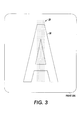
- Figure 3 shows the image data generated by scanning a front side of an image bearing substrate image that includes show-through image information of an image from the back side of the image bearing substrate.
- the vertical line 20 shows through from the back side of the image bearing substrate and is present in the image data of the image 30 of the letter "A" generated from scanning the front side of the image bearing substrate.
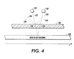
- Figure 4 illustrates the light paths that occur when scanning a translucent image bearing substrate using a non-black backing.
- the translucent image bearing substrate does not have any images formed on it.
- Light 122 from a light source 120 is directed upon the translucent image bearing substrate 130.
- the light 122 from the light source 120 is incident on the front surface of the image bearing substrate 130.
- Portions 124 of the light 122 are scattered by the image bearing substrate 130.
- Other portions 126 of the light 122 are transmitted through the translucent image bearing substrate 130.
- Fig. 4 shows the reflected light 126 being reflected at a large angle, in actuality this angle is quite small and is considered to be zero.
- the figure is illustrative only and is not meant to be limiting in any way.
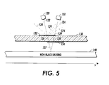
- Figure 5 illustrates the light paths that occur when scanning an image bearing substrate that has images formed on the front and back sides.
- the following discussion assumes that the front and back side images are black and white images. However, as will be apparent to one of ordinary skill in the art, similar light paths will occur with color or grayscale images.
- the light 122 from the light source 120 is incident on the image bearing substrate 130. Portions 124 of the light 122 are scattered by the front side of the image bearing substrate 130. The remaining portion 126 of the light 122 is transmitted through the front side. The fractions of the light 122 that are scattered and that are transmitted depends on the characteristics of the image formed on the front side of the image bearing substrate 130.
- the portion 126 of the light 122 transmitted through the front side of the image bearing substrate 130 is then transmitted through the back side of the image bearing substrate 130.
- the portion 127 of the light 122 that is transmitted through the back side of the image bearing substrate is dependent on the characteristics of the image on the back side of the image bearing substrate and the image bearing substrate itself.
- the transmitted portion 127 of the light 122 is then reflected back from the backing 140 through the back and front sides of the image bearing substrate to the optical sensor 150.
- the portion 128 of the light 122 represents the portion of light that is transmitted through the back side of the image bearing substrate. Portion 128 may not be the same as portion 127 since some of the portion 127 of light 122 may be absorbed by the non-black backing 140 or may be scattered by the back side of the image bearing substrate 130.
- the portion 129 of the light 122 represents the portion of light passing through the front side of the image bearing substrate 130. This portion 129 may not be the same as portion 128 due to, for example, the spread of light through the image bearing substrate 130.
- the "show-through compensated image” that is to be recovered is the image that would have been obtained from the optical sensor if there was no image on the back side of the image bearing substrate. This assumption is only for descriptive purposes and is not intended to limit the scope of the invention. Alternate definitions of the "show-through compensated image” may be used without departing from the spirit and scope of the present invention.
- Paper is close to white in color because paper scatters much more light than it transmits.
- the squared transmittance fraction T p 2 of the light is very small compared to the fraction scattered S p of the light. This allows the following approximation, for values of x having magnitudes much smaller than 1: ln(1-x) ⁇ -x
- the scanned density of the front side image layer D f s (x, y) is a linear combination of the show-through compensated density of the front side image layer D f (x, y) and the show-through compensated absorbency of the back side image layer, A b (x, y).
- Eqs. 6 and 7 can be modified by replacing the term (T p 2 R back /(S p +T p 2 R back )) with a point spread function H(x,y).
- an iterative approach may be used beginning with the above approximation and using the estimated show-through compensated reflectances for computing the absorbencies for the next iteration. These iterations may be repeated for a number of times until acceptable compensation is obtained.
- the show-through point spread function H(x, y) may be approximated using a finite impulse-response (FIR) filter. Since the show-through compensation is linearized, the coefficients for the FIR filter representing H(x, y) can be determined from standard linear prediction theory.
- FIR finite impulse-response
- the show-through point spread function is dependent only on the backing and the image bearing substrate and may be pre-determined or may be estimated by using a region of the image with printing only on the back-side in accordance with optimal linear filtering theory.
- adaptive linear prediction filters may be used.
- the filter representing the show-through point spread function H(x, y) is implemented as an adaptive filter and its coefficients (values for different x and y) are adapted as one moves across the image bearing substrate.
- the density of the show-through compensated image at each x, y location is computed in accordance with Eq. 12.
- the coefficients of the filter are adapted in a direction designed to send estimated D f (x, y) towards zero (note that D f (x, y) is zero in a region with no printing on the front side if there is no show-through).
- adaptive filters has a significant advantage over non-adaptive filters in that the registration of the front and back side images is not required to be extremely precise. As long as the filter size is reasonably large, the filter automatically adapts and compensates for small changes in the registration over the image bearing substrate.
- the adaptive method is also beneficial in that it can account for variations in the show-through point spread function due to the spatial variations in the transmittance of the image bearing substrate.
- D f (x, y) and D b (x, y) represent the normalized densities for the show-through compensated images of the front and back side of the image bearing substrate. These values may be transformed into alternate representations of the show-through compensated images, such as the reflectance representation obtained as the inverse of Eq.
- R f (x, y) ⁇ R p w exp(-D f (x, y))
- R,(x, y) is a close approximation to the image that the optical sensor would have sensed on the front side if there were no printing on the back side
- R b (x, y) is a close approximation to the image that the optical sensor would have detected on the back side if there were no printing on the front side.
- the show-through compensation only needs local information from corresponding front and back side images and therefore does not require the complete front and back side images to be stored in memory (in a device that scans front and back sides simultaneously the delay introduced by the processing would be only a few scan lines).
- the show-through adjusted image data is stored in memory and may also be stored in the image data source 300 for later use in outputting the image using, for example, the image output device 400.
- Figure 6 is a flowchart outlining one exemplary embodiment of a method of compensating for show-through image information in image data. As shown in Fig. 6, beginning in step S500, control continues to step S600, where the image data is input. Next, in step S700, the image data is stored. Then, in step S800, if necessary, the image data is aligned. Control then continues to step S900.
- step S900 the image data is adjusted to remove any show-through image information. Then, in step S1000, the adjusted image data is stored. Next, in step S1100, the control routine ends.
- FIG. 7 is a flowchart outlining one exemplary embodiment of the method for adjusting the image data of step S900 of Fig. 6. As shown in Fig. 7, beginning in step S900, control continues to step S910, where the scanned densities of the front and back sides of the image bearing substrate are determined based on the image data from the front and back side images. As described above, this may be done using the detected reflectances and Eq. 4 for the front side and a corresponding equation for the back side, for example.
- step S920 the absorbencies of the front and back sides of the image bearing substrate are approximated. This may be done, for example, using Eqs. 14 and 15.
- step S930 the show-through point spread function of the image bearing substrate is estimated. As described above, this approximation may be performed automatically using linear prediction filters to approximate the show-through point spread function. Control then continues to step S940.
- step S940 densities for show-through compensated front and back sides of the image bearing substrate are determined from the scanned densities, the approximated absorbencies, and the estimated show-through point spread function. This may be done, for example using Eqs. 12 and 13.
- step S950 show-through compensated reflectances for the front and the back side images are computed, for example, by using Eqs. 16 and 17.
- step S960 control returns to step S1000 in Fig. 6.
- the show-through image information removal device 200 may be implemented on a general purpose or special purpose computer. However, the show-through image information removal device 200 can also be implemented on a programmed microprocessor or microcontroller and peripheral integrated circuit elements, an ASIC or other integrated circuit, a hardware electronic or logic circuit such as a discrete element circuit, a programmable logic device such as a PLD, PLA, FPGA or PAL, or the like. In general, any device on which a finite state machine capable of implementing the flowcharts shown in Figs. 6 and 7 can be used to implement the show-through image information removal device 200 of this invention..
Landscapes
- Engineering & Computer Science (AREA)
- Multimedia (AREA)
- Signal Processing (AREA)
- Image Processing (AREA)
- Editing Of Facsimile Originals (AREA)
- Facsimile Image Signal Circuits (AREA)
Applications Claiming Priority (2)
| Application Number | Priority Date | Filing Date | Title |
|---|---|---|---|
| US09/200,984 US6288798B1 (en) | 1998-11-30 | 1998-11-30 | Show-through compensation apparatus and method |
| US200984 | 1998-11-30 |
Publications (3)
| Publication Number | Publication Date |
|---|---|
| EP1006713A2 true EP1006713A2 (de) | 2000-06-07 |
| EP1006713A3 EP1006713A3 (de) | 2001-09-12 |
| EP1006713B1 EP1006713B1 (de) | 2004-04-14 |
Family
ID=22743998
Family Applications (1)
| Application Number | Title | Priority Date | Filing Date |
|---|---|---|---|
| EP99309373A Expired - Lifetime EP1006713B1 (de) | 1998-11-30 | 1999-11-24 | Vorrichtung und Verfahren zur Durchscheinkorrektur |
Country Status (4)
| Country | Link |
|---|---|
| US (2) | US6288798B1 (de) |
| EP (1) | EP1006713B1 (de) |
| JP (1) | JP4286412B2 (de) |
| DE (1) | DE69916407T2 (de) |
Cited By (1)
| Publication number | Priority date | Publication date | Assignee | Title |
|---|---|---|---|---|
| GB2459675A (en) * | 2008-04-30 | 2009-11-04 | Hewlett Packard Development Co | Double sided substrate scanning |
Families Citing this family (21)
| Publication number | Priority date | Publication date | Assignee | Title |
|---|---|---|---|---|
| JP3325243B2 (ja) * | 1999-09-20 | 2002-09-17 | 京セラミタ株式会社 | 画像処理装置 |
| US6862117B1 (en) * | 1999-12-30 | 2005-03-01 | Eastman Kodak Company | Method and apparatus for reducing the effect of bleed-through on captured images |
| US6999212B2 (en) * | 2001-07-10 | 2006-02-14 | Che-Kuei Mai | Back-light module for image scanning device and method for calibrating illumination with the back-light module |
| US6952293B2 (en) * | 2001-08-31 | 2005-10-04 | Sharp Laboratories Of America, Inc. | Document backing surface for show-through and artifact reduction |
| US7209599B2 (en) * | 2002-07-12 | 2007-04-24 | Hewlett-Packard Development Company, L.P. | System and method for scanned image bleedthrough processing |
| US6877659B2 (en) * | 2002-10-04 | 2005-04-12 | Xerox Corporation | Gyricon platen cover for show-through correction |
| CN100419778C (zh) * | 2003-04-07 | 2008-09-17 | 纳幕尔杜邦公司 | 用于量化平面对象反面上的印刷图像的可视透背的方法和设备 |
| US7327496B2 (en) * | 2003-04-11 | 2008-02-05 | Hewlett-Packard Development Company, L.P. | Imaging apparatus and method |
| TWI252031B (en) * | 2004-05-18 | 2006-03-21 | Avision Inc | Duplex scan method capable of quickly detecting a document size |
| US7728844B2 (en) * | 2004-07-09 | 2010-06-01 | Nokia Corporation | Restoration of color components in an image model |
| JP2006215964A (ja) * | 2005-02-07 | 2006-08-17 | Toshiba Corp | 文字認識装置 |
| US7620360B2 (en) * | 2005-05-20 | 2009-11-17 | Lexmark International, Inc. | Method for reducing show-through in a scanned duplexed document |
| US7620359B2 (en) * | 2005-05-20 | 2009-11-17 | Lexmark International, Inc. | Method for processing a duplexed document |
| US7623725B2 (en) * | 2005-10-14 | 2009-11-24 | Hewlett-Packard Development Company, L.P. | Method and system for denoising pairs of mutually interfering signals |
| KR100888600B1 (ko) * | 2007-04-03 | 2009-03-16 | 삼성전자주식회사 | 스캐닝된 이미지의 뒷 비침 제거 방법 및 장치 |
| US7965421B2 (en) * | 2008-04-16 | 2011-06-21 | Xerox Corporation | Show-through reduction method and system |
| JP4395538B2 (ja) * | 2008-04-24 | 2010-01-13 | 三菱重工業株式会社 | インキの発色が透過してしまう現象により生じる透過現象発色値の推定方法及び装置、インキの発色が透過してしまう現象を考慮した発色値推定方法及び装置、インキの発色が透過してしまう現象を考慮した目標色設定方法及び装置、並びに印刷機の制御方法及び装置 |
| US8503733B2 (en) * | 2009-11-16 | 2013-08-06 | Xerox Corporation | Show-through measurement system and method for inks on media |
| US8553944B2 (en) | 2010-06-14 | 2013-10-08 | Seiko Epson Corporation | Removing leakage from a double-sided document |
| IL219813B (en) * | 2012-05-01 | 2019-07-31 | Matan Digital Printing Ltd | Superimposing images on translucent media |
| EP4480711A1 (de) * | 2023-06-21 | 2024-12-25 | Canon Production Printing Holding B.V. | Verfahren zum drucken eines prüfbildes |
Family Cites Families (8)
| Publication number | Priority date | Publication date | Assignee | Title |
|---|---|---|---|---|
| JP2504037B2 (ja) * | 1987-03-18 | 1996-06-05 | 日本電気株式会社 | フアクシミリ装置 |
| JPH06225145A (ja) * | 1993-01-22 | 1994-08-12 | Yamatoya & Co Ltd | 画像の階調変換法 |
| US5677776A (en) * | 1994-09-29 | 1997-10-14 | Minolta Co., Ltd. | Image reader for processing an image of a document |
| US5646744A (en) * | 1996-01-11 | 1997-07-08 | Xerox Corporation | Show-through correction for two-sided documents |
| JPH09200455A (ja) * | 1996-01-19 | 1997-07-31 | Minolta Co Ltd | 読取り画像の濃度補正方法及び画像読取り装置 |
| JPH09205544A (ja) * | 1996-01-26 | 1997-08-05 | Minolta Co Ltd | 読取り画像の修正方法及び画像読取り装置 |
| US6067385A (en) * | 1997-05-07 | 2000-05-23 | Ricoh Company Limited | System for aligning document images when scanned in duplex mode |
| US6101283A (en) * | 1998-06-24 | 2000-08-08 | Xerox Corporation | Show-through correction for two-sided, multi-page documents |
-
1998
- 1998-11-30 US US09/200,984 patent/US6288798B1/en not_active Expired - Lifetime
-
1999
- 1999-11-24 EP EP99309373A patent/EP1006713B1/de not_active Expired - Lifetime
- 1999-11-24 DE DE69916407T patent/DE69916407T2/de not_active Expired - Lifetime
- 1999-11-30 JP JP33893099A patent/JP4286412B2/ja not_active Expired - Fee Related
-
2000
- 2000-09-27 US US09/671,393 patent/US7145697B1/en not_active Expired - Lifetime
Cited By (2)
| Publication number | Priority date | Publication date | Assignee | Title |
|---|---|---|---|---|
| GB2459675A (en) * | 2008-04-30 | 2009-11-04 | Hewlett Packard Development Co | Double sided substrate scanning |
| EP2280832A4 (de) * | 2008-04-30 | 2014-01-15 | Hewlett Packard Development Co |
Also Published As
| Publication number | Publication date |
|---|---|
| DE69916407D1 (de) | 2004-05-19 |
| US6288798B1 (en) | 2001-09-11 |
| EP1006713B1 (de) | 2004-04-14 |
| DE69916407T2 (de) | 2004-09-09 |
| JP2000175017A (ja) | 2000-06-23 |
| JP4286412B2 (ja) | 2009-07-01 |
| EP1006713A3 (de) | 2001-09-12 |
| US7145697B1 (en) | 2006-12-05 |
Similar Documents
| Publication | Publication Date | Title |
|---|---|---|
| EP1006713B1 (de) | Vorrichtung und Verfahren zur Durchscheinkorrektur | |
| US6101283A (en) | Show-through correction for two-sided, multi-page documents | |
| US5371615A (en) | Image-dependent color correction using black point and white point in a natural scene pictorial image | |
| US7064868B2 (en) | Image processor | |
| US6671068B1 (en) | Adaptive error diffusion with improved edge and sharpness perception | |
| EP0838942A2 (de) | Verfahren und Vorrichtung zur Belichtungseinstellung eines ausgewählten Bereiches | |
| US20020097439A1 (en) | Edge detection and sharpening process for an image | |
| JP3706185B2 (ja) | 画像再生方法および装置 | |
| JPH09200528A (ja) | 画像処理方法及び画像処理装置 | |
| EP0402162B1 (de) | Bildverarbeitung mit Rauschanreicherungsoperatoren für Moiré-Verringerung und/oder Zufallspunkterzeugung | |
| JPH05161025A (ja) | カラー画像処理装置のパターン発生方式 | |
| JP2710310B2 (ja) | 絵画原稿のコピーの電子的プリント方法 | |
| JPH0568146B2 (de) | ||
| JP3954139B2 (ja) | デジタル写真プリンタ | |
| JPH0722341B2 (ja) | 偽画像除去方法 | |
| JP4656648B2 (ja) | デジタル撮像装置,画像読み取り装置および画像形成装置 | |
| JP2000209396A (ja) | 画像読取方法および装置 | |
| JPH10108018A (ja) | 画像処理装置及び画像処理方法、並びに画像形成装置 | |
| JP3253117B2 (ja) | 画像処理装置および方法 | |
| JP4024737B2 (ja) | 画像処理装置、画像読取装置、画像形成装置、画像処理方法、およびプログラム | |
| JP4085932B2 (ja) | 画像形成装置 | |
| EP1562144B1 (de) | Bildverarbeitungsvorrichtung und Bildverarbeitungsverfahren zur Korrektur von Bilddaten | |
| US7746509B2 (en) | Method for removing defects in scanned images | |
| JP3696463B2 (ja) | 画像処理装置 | |
| JP3267575B2 (ja) | 画像処理方法 |
Legal Events
| Date | Code | Title | Description |
|---|---|---|---|
| PUAI | Public reference made under article 153(3) epc to a published international application that has entered the european phase |
Free format text: ORIGINAL CODE: 0009012 |
|
| AK | Designated contracting states |
Kind code of ref document: A2 Designated state(s): AT BE CH CY DE DK ES FI FR GB GR IE IT LI LU MC NL PT SE Kind code of ref document: A2 Designated state(s): DE FR GB |
|
| AX | Request for extension of the european patent |
Free format text: AL;LT;LV;MK;RO;SI |
|
| PUAL | Search report despatched |
Free format text: ORIGINAL CODE: 0009013 |
|
| AK | Designated contracting states |
Kind code of ref document: A3 Designated state(s): AT BE CH CY DE DK ES FI FR GB GR IE IT LI LU MC NL PT SE |
|
| AX | Request for extension of the european patent |
Free format text: AL;LT;LV;MK;RO;SI |
|
| 17P | Request for examination filed |
Effective date: 20020312 |
|
| AKX | Designation fees paid |
Free format text: DE FR GB |
|
| 17Q | First examination report despatched |
Effective date: 20020920 |
|
| GRAP | Despatch of communication of intention to grant a patent |
Free format text: ORIGINAL CODE: EPIDOSNIGR1 |
|
| GRAS | Grant fee paid |
Free format text: ORIGINAL CODE: EPIDOSNIGR3 |
|
| GRAA | (expected) grant |
Free format text: ORIGINAL CODE: 0009210 |
|
| AK | Designated contracting states |
Kind code of ref document: B1 Designated state(s): DE FR GB |
|
| REG | Reference to a national code |
Ref country code: GB Ref legal event code: FG4D |
|
| REF | Corresponds to: |
Ref document number: 69916407 Country of ref document: DE Date of ref document: 20040519 Kind code of ref document: P |
|
| ET | Fr: translation filed | ||
| PLBE | No opposition filed within time limit |
Free format text: ORIGINAL CODE: 0009261 |
|
| STAA | Information on the status of an ep patent application or granted ep patent |
Free format text: STATUS: NO OPPOSITION FILED WITHIN TIME LIMIT |
|
| 26N | No opposition filed |
Effective date: 20050117 |
|
| PGFP | Annual fee paid to national office [announced via postgrant information from national office to epo] |
Ref country code: FR Payment date: 20131121 Year of fee payment: 15 Ref country code: GB Payment date: 20131025 Year of fee payment: 15 Ref country code: DE Payment date: 20131022 Year of fee payment: 15 |
|
| REG | Reference to a national code |
Ref country code: DE Ref legal event code: R119 Ref document number: 69916407 Country of ref document: DE |
|
| GBPC | Gb: european patent ceased through non-payment of renewal fee |
Effective date: 20141124 |
|
| REG | Reference to a national code |
Ref country code: FR Ref legal event code: ST Effective date: 20150731 |
|
| PG25 | Lapsed in a contracting state [announced via postgrant information from national office to epo] |
Ref country code: GB Free format text: LAPSE BECAUSE OF NON-PAYMENT OF DUE FEES Effective date: 20141124 Ref country code: DE Free format text: LAPSE BECAUSE OF NON-PAYMENT OF DUE FEES Effective date: 20150602 |
|
| PG25 | Lapsed in a contracting state [announced via postgrant information from national office to epo] |
Ref country code: FR Free format text: LAPSE BECAUSE OF NON-PAYMENT OF DUE FEES Effective date: 20141201 |