EP1007754B1 - Depot de minces films avec angle de reflexion - Google Patents
Depot de minces films avec angle de reflexion Download PDFInfo
- Publication number
- EP1007754B1 EP1007754B1 EP98936049A EP98936049A EP1007754B1 EP 1007754 B1 EP1007754 B1 EP 1007754B1 EP 98936049 A EP98936049 A EP 98936049A EP 98936049 A EP98936049 A EP 98936049A EP 1007754 B1 EP1007754 B1 EP 1007754B1
- Authority
- EP
- European Patent Office
- Prior art keywords
- substrate
- thin film
- vapor
- flux
- vapor flux
- Prior art date
- Legal status (The legal status is an assumption and is not a legal conclusion. Google has not performed a legal analysis and makes no representation as to the accuracy of the status listed.)
- Expired - Lifetime
Links
Images



Classifications
-
- C—CHEMISTRY; METALLURGY
- C23—COATING METALLIC MATERIAL; COATING MATERIAL WITH METALLIC MATERIAL; CHEMICAL SURFACE TREATMENT; DIFFUSION TREATMENT OF METALLIC MATERIAL; COATING BY VACUUM EVAPORATION, BY SPUTTERING, BY ION IMPLANTATION OR BY CHEMICAL VAPOUR DEPOSITION, IN GENERAL; INHIBITING CORROSION OF METALLIC MATERIAL OR INCRUSTATION IN GENERAL
- C23C—COATING METALLIC MATERIAL; COATING MATERIAL WITH METALLIC MATERIAL; SURFACE TREATMENT OF METALLIC MATERIAL BY DIFFUSION INTO THE SURFACE, BY CHEMICAL CONVERSION OR SUBSTITUTION; COATING BY VACUUM EVAPORATION, BY SPUTTERING, BY ION IMPLANTATION OR BY CHEMICAL VAPOUR DEPOSITION, IN GENERAL
- C23C14/00—Coating by vacuum evaporation, by sputtering or by ion implantation of the coating forming material
- C23C14/22—Coating by vacuum evaporation, by sputtering or by ion implantation of the coating forming material characterised by the process of coating
- C23C14/225—Oblique incidence of vaporised material on substrate
- C23C14/226—Oblique incidence of vaporised material on substrate in order to form films with columnar structure
-
- C—CHEMISTRY; METALLURGY
- C03—GLASS; MINERAL OR SLAG WOOL
- C03C—CHEMICAL COMPOSITION OF GLASSES, GLAZES OR VITREOUS ENAMELS; SURFACE TREATMENT OF GLASS; SURFACE TREATMENT OF FIBRES OR FILAMENTS MADE FROM GLASS, MINERALS OR SLAGS; JOINING GLASS TO GLASS OR OTHER MATERIALS
- C03C17/00—Surface treatment of glass, not in the form of fibres or filaments, by coating
- C03C17/001—General methods for coating; Devices therefor
-
- C—CHEMISTRY; METALLURGY
- C23—COATING METALLIC MATERIAL; COATING MATERIAL WITH METALLIC MATERIAL; CHEMICAL SURFACE TREATMENT; DIFFUSION TREATMENT OF METALLIC MATERIAL; COATING BY VACUUM EVAPORATION, BY SPUTTERING, BY ION IMPLANTATION OR BY CHEMICAL VAPOUR DEPOSITION, IN GENERAL; INHIBITING CORROSION OF METALLIC MATERIAL OR INCRUSTATION IN GENERAL
- C23C—COATING METALLIC MATERIAL; COATING MATERIAL WITH METALLIC MATERIAL; SURFACE TREATMENT OF METALLIC MATERIAL BY DIFFUSION INTO THE SURFACE, BY CHEMICAL CONVERSION OR SUBSTITUTION; COATING BY VACUUM EVAPORATION, BY SPUTTERING, BY ION IMPLANTATION OR BY CHEMICAL VAPOUR DEPOSITION, IN GENERAL
- C23C14/00—Coating by vacuum evaporation, by sputtering or by ion implantation of the coating forming material
- C23C14/22—Coating by vacuum evaporation, by sputtering or by ion implantation of the coating forming material characterised by the process of coating
-
- C—CHEMISTRY; METALLURGY
- C23—COATING METALLIC MATERIAL; COATING MATERIAL WITH METALLIC MATERIAL; CHEMICAL SURFACE TREATMENT; DIFFUSION TREATMENT OF METALLIC MATERIAL; COATING BY VACUUM EVAPORATION, BY SPUTTERING, BY ION IMPLANTATION OR BY CHEMICAL VAPOUR DEPOSITION, IN GENERAL; INHIBITING CORROSION OF METALLIC MATERIAL OR INCRUSTATION IN GENERAL
- C23C—COATING METALLIC MATERIAL; COATING MATERIAL WITH METALLIC MATERIAL; SURFACE TREATMENT OF METALLIC MATERIAL BY DIFFUSION INTO THE SURFACE, BY CHEMICAL CONVERSION OR SUBSTITUTION; COATING BY VACUUM EVAPORATION, BY SPUTTERING, BY ION IMPLANTATION OR BY CHEMICAL VAPOUR DEPOSITION, IN GENERAL
- C23C14/00—Coating by vacuum evaporation, by sputtering or by ion implantation of the coating forming material
- C23C14/22—Coating by vacuum evaporation, by sputtering or by ion implantation of the coating forming material characterised by the process of coating
- C23C14/50—Substrate holders
- C23C14/505—Substrate holders for rotation of the substrates
Definitions
- This invention relates to the deposition of shadow sculpted thin films on substrates.
- optical properties of the resulting microstructure are dependent in part on the material used, the porosity of the microstructure and the orientation of the columns of the thin film.
- Hamaguchi et al United States patent no. 4,874,664, describe lateral shifting or rotation of the position of the substrate in relation to the vapor flux to create uniform film growth and film layers that have columns with different orientations in the different layers.
- the entire substrate is rotated in between periods of exposure of the substrate to vapor flux, or the substrate is laterally shifted during exposure to vapor flux.
- the inventors have proposed improvements to the methods of Azzam and Hamaguchi, as described in "First thin film realization of a helicoidal bianisotropic medium", Kevin Robbie and Michael J. Brett, Akhlesh Lakhtakia, J. Vac. Sci. Technol. A 18(6), Nov/Dec 1995, p. 2991 - 2993.
- the substrate may be rotated an integral number of times, or, to create a helical pattern, rotated nearly an integral a number of times and paused between periods of rotation at sequentially offset positions.
- An optical filter may thus be made with plural thin film layers, wherein each thin film layer is formed by repeating steps A and B.
- the rotation speed of the direction of arrival of the vapor flux at the substrate during step A is sufficiently high that the direction of arrival of the vapor flux at the substrate rotates at least once within the time required for the thin film to grow a distance, measured normal to the substrate, substantially equal to the adatom diffusion length of the material being deposited.
- a microstructure comprising a first thin film of plural columns extending from a surface of a substrate, wherein the columns are formed under a given set of conditions by vapor deposition on the surface of the substrate from vapor flux incident at an angle ⁇ f to a normal to the surface of the substrate, where 0° ⁇ ⁇ f ⁇ 90°, the vapor being deposited at least in part while the direction of arrival of the vapor flux at the substrate is rotating, and the columns exhibit the property that 0° ⁇ ⁇ c ⁇ ⁇ n where ⁇ c is the angle between the columns and a normal to the surface of the substrate and ⁇ n is the angle at which the columns would grow under the given set of conditions without rotation of the direction of arrival of the vapor flux at the substrate.
- the columns are formed at least in part while the direction of arrival of the vapor flux at the substrate is rotating at a rotation speed that is sufficiently high that the direction of arrival of the vapor flux at the substrate rotates at least once within the time required for the thin film to grow a distance, measured normal to the substrate, substantially equal to the adatom diffusion length of the material being deposited.
- a second thin film may be formed on top of the first thin film with a different porosity, which may be created by deposition of the second thin film with a different incident angle of vapor flux than the incident angle ⁇ f for the first thin film.
- the plural thin films may form a continuous stack of thin film layers, one of the plural thin film layers being placed against the top of the first thin film, with each thin film layer having a different porosity from adjacent thin film layers.
- the thin film may have an refractive index that varies with distance from the substrate.
- the oblique incident angle of vapor flux is varied to produce alternating bands of high and low density material deposited on the substrate.
- “Oblique” as used in this patent document in relation to an angle means sufficiently departing from 0° that atomic shadowing has a significant effect on the growth of columnar microstructures.
- the resultant thin films do not have particularly useful properties.
- the inventors have found that for angles of incidence of vapor flux greater than 70° and even more so at 80° and greater, the resultant thin films have well defined structures with useful properties.
- the direction of arrival of an obliquely incident vapor flux at a substrate is the direction in the plane of the substrate obtained by a projection, normal to the substrate, of the angle of incidence onto the substrate.
- Rotation of the direction of arrival of the vapor flux at the substrate is obtained typically, and most easily, by rotation of the substrate, whereby the direction of arrival of the vapor flux at the substrates rotates around a normal to the substrate.
- the invention will be described, in the illustrative embodiment for the case when the substrate itself rotates.
- the substrate may be any solid material on which a vapor may be deposited, and will depend on the application. Silicon and glass substrates will be commonly used.
- the material to be deposited may be any material for which conditions are achievable to support vapor generation and deposition of the vaporized material on the substrate. In some cases, this may require cooling or heating of the substrate.
- an intervening layer may be first deposited, as for example using a chromium intermediate layer to bond gold to amorphous silicon dioxide (glass). The processes described here should be carried out in conditions in which the vapor flux arrives at the substrate in approximately a straight line.
- the process be carried out under conditions approximating a vacuum, at less than 0.13N/m 2 (10 -3 torr), for example at 1.3x10 -4 N/m 2 (10 -6 torr).
- a vacuum at less than 0.13N/m 2 (10 -3 torr), for example at 1.3x10 -4 N/m 2 (10 -6 torr).
- scattering from gas molecules tends to prevent well defined structures from growing.
- the material used should have a sticking co-efficient of at least about 0.9 to enable the formation of distinct structures.
- the growth direction of a column of material is along the axis of the column away from the substrate from which the column is growing. In the case of a helical column, in which the helical structure follows the surface of a hypothetical cylinder, the axis of the column is the axis of the cylinder.
- Fig. 1A illustrates the physical process underlying growth of a slanted columnar film microstructure as is known in the prior art.
- a substrate 10 for example a silicon wafer, has a surface 12 with normal N and is exposed to an oblique incident vapor flux 14 whose angle of incidence, defined in relation to the normal N, is ⁇ f .
- atoms in the vapor flux 14 are deposited onto the substrate 10, film growth areas atoms shadow adjacent regions 16, preventing deposition of vapor in these regions.
- Atoms in the vapor flux 14 continue to be deposited in regions that are not shadowed, thus forming columns 18.
- Adatoms diffuse atomically across the tops of the columns as shown at 19. Slanted columnar microstructures will grow if the angle ⁇ f is sufficiently large to create the shadowing effect, and there is limited adatom diffusion 19, such that adatom diffusion does not fill in the gaps between columns.
- the growth conditions under which a columnar thin film grows on a substrate include the substrate temperature (typically from about 77°K to 600°K), pressure of the vessel in which the vapor deposition takes place, vapor flux intensity (which depends upon the proximity of the vapor source to the substrate and the evaporation rate), vapor flux energy (which depends on the manner in which the vapor flux is created, for example by sputtering or heating), type of material used to produce the vapor flux, for example Cu, MgF 2 , CaF 2 , SiO, Al, Mn, Cr, Ag, Si, Co, ZrO 2 , Ti and PermalloyTM (85% nickel, 15% iron alloy), rotation speed of the substrate, angle of incidence of the vapor flux and the nature of the background gas in the vessel, which is typically maintained at a very low pressure.
- Fig. 2 These three results of film structure with incident flux angle are summarized in Fig. 2 where the columnar growth angle is graphed against the vapor flux arrival angle.
- the solid line is calculated from Tait's rule.
- Points 2 and 3 correspond to Fig. 1C and 1D respectively.
- film microstructures are confined to points on this line.
- the column angle and porosity are fixed (for a given material and set of deposition conditions).
- GLAD glancing angle deposition
- the growth of this film can be thought of as resulting from the sum of the growth caused by the vapor flux from one side and the growth caused by the flux from the other side.
- the quantity of the flux from each side is chosen to be substantially equal (50% of the total from each side).
- the amount of flux from one side is chosen to be between 50% and 100%.
- Fig. 5 shows this result. With 70% of the flux from one side and 30% of the flux from the other, the column angle is more vertical than with the one sided flux case (100% from one side - Fig.
- helix pattern may be obtained at slower rotation speeds if the remaining small helical structure is not detrimental to a specific application.
- Exemplary diffusion lengths for unheated substrates are: MgF 2 - 60 nm; Cu - 150 nm, Cr - 90 nm, Mn - 80 nm and Al - 100 nm.
- Substrate rotation at a speed sufficient to functionally eliminate the inherent helical structure may be called spinning growth.
- the helical structure of the columns is functionally eliminated
- the electromagnetic radiation includes radiation having a frequency ⁇ and the electromagnetic radiation is propagating along a light path.
- An optical filter may be placed in the light path, in which the optical filter has plural helical columns extending from a substrate. The effect of the columns is functionally eliminated if the helical columns each have a pitch p sufficiently smaller than that propagation of light is unaffected by the helical structure of the columns.
- the helical columns may have a larger helical geometry or may be arranged with a varying index of refraction that the optical filter has other useful properties that is not dependent on the small scale helical geometry of the columns.
- the small scale helical columns will not affect light propagation when p ⁇ ⁇ /4, particularly when p ⁇ ⁇ /10.
- Spinning growth effectively provides a flux distribution that is substantially equal from all directions around the substrate while the polar angle ⁇ f remains fixed - analogous to Fig. 4 and the columns grow in a growth direction that is perpendicular to the surface of the substrate.
- Inclined growth in a growth direction offset from the vertical is produced by altering one of the growing conditions, namely reducing the substrate rotation speed so that the substrate is effectively held in place and not rotating (call this paused growth - analogous to Fig. 1D). Minor deviations from exactly zero rotation speed are permissible, providing the overall effect is to produce an offset growth direction (that is, the growth direction is not the same as during the preceding deposition period).
- the column then begins to grow conventionally slanted towards the vapor source, though at a steeper angle than ⁇ f .
- a second portion of the thin film is formed which has a different growth direction than the growth direction in which the portion of the column grows during spinning growth. Repetition of spinning growth and paused growth causes the column to grow with an angle ⁇ c that is less than ⁇ n , the angle at which the columns would grow under the same growing conditions without rotation of the substrate.
- Spinning and paused growth conditions are illustrated with the plan view of the substrate in Fig. 7.
- the small single arrows A depict the flux arriving from all directions while the substrate is spinning quickly (spinning growth).
- the double arrow B depicts the second type of growth where the substrate is fixed and a columnar structure inclined toward the vapor source is produced (paused growth).
- Control over the structure comes from choosing how long to pause relative to the time for one revolution and from choosing the pause position.
- the type of deposition can be described by the percentage of the flux that arrives during the paused and spinning growth conditions.
- the substrate is typically rotated an integral number of times, for example, once.
- a common structure produced with conventional GLAD is a helical columnar film.
- the film was deposited with the advanced precessing technique with spinning growth (with a pitch of 100nm forming larger helical columns) used for 50% of the deposition time and precessing paused growth (with a pitch of about 1 ⁇ m) used for 50% of the deposition time.
- ⁇ c ⁇ 15°
- this structure is similar to the inner helix of Fig. 8. This is a structure which could not be obtained with conventional GLAD and demonstrates the ability of the precessional method for controlling thin film microstructures.
- FIG. 9, 10 and 11 an apparatus according to the invention is shown for growing a thin film on a substrate 10 having a surface 12.
- a conventional vapor source 22 is located within a vacuum chamber 20.
- a conventional shutter (not shown) located above the vapor source 22 is used to control whether or not the substrate 10 is exposed to vapor.
- Various conventional means (not shown separately) for causing the vapor source 22 to emit a vapor flux 14 may be used.
- a substrate 10 is supported in the vacuum chamber 20 on a motor 24 (Fig. 11A) disposed in the vacuum chamber 20 above the vapor source 22. The motor 24 rotates the substrate about an axis A lying parallel to and preferably in the plane defined by the surface 12 of the substrate 10.
- Rotation of the substrate 10 about axis A alters the polar angle, namely the angle of incidence ⁇ of the vapor flux 14.
- Motor 26, also disposed in the vacuum chamber 20 above the vapor source 22, has a rotational axis coinciding with the normal N of the substrate 10 and thus alters the azimuthal angle.
- the polar angle and the azimuthal angles are both measures of the orientation of the surface of the substrate to the incident flux.
- the substrate 10 is preferably mounted on a disc 11 which is attached to motor 26.
- motor 26 may be mounted on a frame 25, and the frame 25 may be mounted to rotate with the drive shaft 27 of motor 24.
- Motor 24 itself may be mounted by any of various conventional methods for mounting motors within a vacuum chamber such as on a support 29.
- motors 24 and 26 are preferably conventional stepper motors driven by stepper motor drive electronics 28 and controlled by computer controller 30.
- the computer controller 30 includes a data acquisition board 32 and a software based interface 34 such as LabVIEWTM available from National Instruments. Software for implementing the invention is disclosed in applicant's Canadian priority application filed May 16, 1998, as application no. 2,237,732, and is available from WIPO or CIPO after publication or upon request from the inventors at the University of Alberta, Canada.
- the data acquisition board 32 receives signals indicative of thin film growth on the substrate output from a deposition rate monitor 36 of conventional construction located within the vacuum chamber 20 in a location in which film growth on the deposition rate monitor 36 is representative of film growth on the substrate 10.
- the computer controller 30 instructs the driver 28 to cause the motors 24 and 26 to rotate according to a desired pattern.
- the computer automatically controls the rate of change of the orientation of the surface in response to the output control signals to grow the thin film according to the desired pattern.
- Start and stop signals for vapor deposition may be sent by the computer to a drive for the shutter for starting vapor deposition, or the shutter may be opened manually. Normally, the motors are started before the shutter opens to initiate deposition.
- the software receives a deposition rate from the deposition rate monitor.
- the actual thickness (T2) of the film growing on the substrate is related to the thickness on the deposition rate monitor by an empirically determined scaling factor known as the tooling factor.
- the software also knows the motor positions at the last time instant (Xfi for motor 24, Xci for motor 26) and receives as input from the operator, the number (N) of turns to be made by the motor 26, the tooling factor (ratio of vertical film growth rate to measured deposition rate), an initial deposition rate estimate, an initial angle of incidence for the vapor flux during sculpted film growth, motor rotation direction, and various parameters that define the desired pattern of growth for the film.
- the inputs to the computer establish the desired pattern of film growth.
- the motors 24, 26 are step motors that rotate a fraction of a circle each time instant, ti, ti+1, ti+2 etc.
- the computer has just updated the thickness of the film from the deposition rate monitor 36 and changed the motor step rate so that at ti+1, the motor 24, 26 will be at approximately the desired position according to the desired pattern.
- the software calculates what the thickness of the film growth will be at ti+2 and calculates how fast the motors must rotate in order to give the desired thickness at ti+2.
- the computer then reads the new thickness from the deposition rate monitor as well as the motor stepping rates, and adjusts the motor stepping rate so that at ti+3 the film growth pattern will be approximately as desired.
- the software continues in this fashion until a stop signal is received, for example when the film has reached a desired thickness.
- Rotation speed of the substrate about its normal depends in part on the deposition rate. For MgF 2 at 85° angle of incidence, and a pitch of about 50 nm, the speed is about 2 rpm. Typical rotation speeds used in the process are about 0.2 to 3 rpm.
- Fig. 7A azimuthal rotation rate of the substrate is plotted against time for the case when the column forms a sinusoidally varying structure as illustrated in Fig. 7C.
- Times corresponding to points T1-T4 are illustrated on Fig. 7C.
- the width of the time segments 52 corresponds to the time duration of spinning growth.
- the rotation rate is zero, while the substrate continues to be exposed to vapor flux (paused growth), resulting in the slanted column segments 59.
- the period between the time segments 52 continually decreases from T1 to T3 and then increases from T3 to T4 in an approximately sinusoidally varying manner.
- time segment 54 corresponds to half a rotation and the pause position switches from the one side to another such that the column begins to grow in a different direction.
- the half-rotation at T3 corresponds to altering the direction of flux by 180° as illustrated by the arrows C and D in Fig. 7C.
- the column angle ⁇ c varies with distance (measured perpendicularly) from the substrate.
- azimuthal rotation rate is plotted against time for a helical microstructure that falls within the shaded area of the graph of Fig. 2.
- Each time segment 56 corresponds to a period of rotation. In between the periods of rotation, the substrate rotation is zero (paused) while the substrate continues to be exposed to vapor flux.
- the time segments 56 and the intervals between them are constant during deposition. In this instance, the time segment 56 corresponds to a rotation of about 360 ⁇ n°, which results in an offset growth direction for the columns of thin films at an angle that is determined by the azimuthal angle of incidence of the vapor flux.
- n which may be for example from 2-10, affects both diameter and pitch of the helical structure. That is, for a given pause/spin relation (say 30% spin and 70% pause as a proportion of time for constant deposition rate), increased precession, ie greater n, will give smaller diameter of the helix and smaller pitch. For a given azimuthal precession of pause position (say 362°), increased pause duration in relation to spin duration, will give larger diameter and smaller pitch. In both cases, the tube diameter of the helix (diameter of the strand forming the helix) should remain fairly constant.
- Fig. 7D periods of faster rotation (centered about times T1) for example for one half of a rotation and slower rotation (centered about times T2) for another half a rotation are illustrated.
- the corresponding columnar growth is shown in Fig. 7E, showing the positions on the column 90 corresponding to the times T1 and T2.
- Depositable material is column forming when it exhibits limited adatom diffusion and a sufficiently high sticking factor that structures are formed, rather than unformed masses.
- the substrate need not be heated, but the substrate temperature will rise to about 100°C due to heating from the evaporation source.
- the diffusion length of the MgF 2 under these conditions will be about 40-90 nm.
- the deposition rate on a monitor near the substrate for flux at normal incidence is about 2-6 nm/s.
- fast spinning spininning growth
- Vacuum pressure for growth in these conditions may be about 1.3x10 -4 N/m 2 (1x10 -6 torr).
- the thin film depositional apparatus illustrated in Figs. 9-11A is used together with the principle of spinning growth.
- Vapor flux from the evaporation source arrives at the substrate at a glancing angle ( ⁇ f > 50°).
- the substrate position is controlled by the two stepper motors 24 and 26 inside the vacuum deposition system.
- To generate a film with a density variation with thickness the tilt angle ( ⁇ f ) is varied proportionally to the desired density variation during deposition.
- the axial rotation is rapid during the deposition (spinning growth), generating a vertical porous columnar structure and eliminating the helical columnar structure produced by conventional application of GLAD.
- This deposition process produces an interference filter with index of refraction that varies according to the distance from the substrate, as illustrated in Fig. 13.
- the columns 80 are grown from a substrate 10 with rapid spinning throughout.
- the polar angle ⁇ f is varied, the columns 80 produce layers of greater density as shown at 82 and lower density as shown at 84.
- Layer 82 corresponds to a less oblique incident angle (say 70°) and higher index film
- layer 84 corresponds to a more oblique incident angle (say 85°) and lower index film.
- the layers thus formed have different densities in adjacent layers. It is believed that by calibrating the density (index) as a function of deposition angle any desired index variation may be generated.
- the inventors have found that a simple density weighted sum of the index of a thin film material and the index of air was found to predict accurately the effective refractive index as measured with a prism coupler.
- a film with a sinusoidal variation of refractive index may be varied sinusoidally between 51° and 81° during deposition.
- the axial rotation is rapid during the deposition, generating a vertical porous columnar structure and eliminating the helical columnar structure produced for other applications of GLAD.
- This deposition process has been used to produce a MgF 2 rugate filter, whose measured and theoretically predicted reflectance spectrum is shown in Fig. 14.
- the deposition angle variation is sinusoidal, the density as a function of oblique deposition angle is nonlinear and it is expected that the density (index) profile is not truly sinusoidal.
- This thickness value is large for thermally evaporated MgF 2 which typically fractures from stress when deposited thicker than about 1 ⁇ m, lending support to the idea that these films have low stress.
- CMM characteristic matrix method
- An optical filter made with a thin film microstructure according to the invention may be tuned using the structure illustrated in Fig. 12.
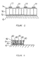
- Vapor deposited material extends in distinct (separate from one another) helical columns 70 from an electrode 72 lying on substrate 10. Electrode 72 may also be located on the other side of substrate 10. The distinct helical columns 70 terminating distally from the substrate 10 in a region of denser material forming a cap 74 for the helical columns.
- the cap 74 may be produced by changing the angle of incidence of the flux from ⁇ near 90° to zero (corresponding to rotation about an axis parallel to the substrate surface), or, it is believed on reasonable grounds that, the deposition of the helical columns may be ended under conditions giving rise to a higher diffusion length, as for example higher substrate temperature or changing to a lower melting point material. Increased substrate temperature may be created by exposing the substrate to light from quartz lamps. Temperatures of within about 100°C to 200°C of the melting point of the material being deposited may be required to create conditions of high diffusion length.
- plural top electrodes 77 may extend in parallel strips across the top of the cap layer 74 or a single electrode may be formed as a single plate on the top of the cap, or the cap may be formed of electrically conducting material to act as an electrode itself.
- the electrodes 72 and 77 may be pulled together or pushed apart and thus change the pitch of the helices 70. This has the effect of tuning the filter created by the thin film.
- Uses for thin films with helical growths also include applications in semiconductor integrated circuit fabrication such as very low dielectric insulators for high speed devices, optical filters, electrical delay lines, biological filters, electroluminescent devices, catalyst supports, thermal barrier coatings on high temperature cycling parts such as jet turbine blades, flat panel displays, thermoelectric cooling panels, solar absorbers, adhesive surfaces, electron emitters, tactile sensing for smart skins, magnetic devices, anti-reflection/low dielectric constant coatings, humidity sensing and microfluid pumping systems.
- semiconductor integrated circuit fabrication such as very low dielectric insulators for high speed devices, optical filters, electrical delay lines, biological filters, electroluminescent devices, catalyst supports, thermal barrier coatings on high temperature cycling parts such as jet turbine blades, flat panel displays, thermoelectric cooling panels, solar absorbers, adhesive surfaces, electron emitters, tactile sensing for smart skins, magnetic devices, anti-reflection/low dielectric constant coatings, humidity sensing and microfluid pumping systems.
- the vapor deposited material When used as helicoidal bianositropic media, the vapor deposited material should be at least partially transparent at the wavelength of the electromagnetic radiation of interest.
- the invention is believed to be able to make structures with utility for filtering light having optical, infrared, microwave and millimeter wavelength.
- the direction of arrival of the vapor flux at the substrate may be obtained by sequential operation of plural vapor sources disposed about the substrate.
- the vapor sources may be located around a hemi-spherical enclosure disposed above a substrate.
- the sources may then be operated (turned on and off) sequentially to cause the vapor to arrive at different directions of arrival.
- the direction of arrival of the vapor flux at the substrate may be rotated in this fashion about a normal to the substrate or the angle of incidence may be changed.
- Other ways of accomplishing the variation in direction of arrival of the vapor flux at the substrate in accordance with the principles of the invention may occur to a person skilled in the art and these are intended to be covered by the claims that follow.
Landscapes
- Chemical & Material Sciences (AREA)
- Organic Chemistry (AREA)
- Engineering & Computer Science (AREA)
- Materials Engineering (AREA)
- Chemical Kinetics & Catalysis (AREA)
- Mechanical Engineering (AREA)
- Metallurgy (AREA)
- General Chemical & Material Sciences (AREA)
- Life Sciences & Earth Sciences (AREA)
- Geochemistry & Mineralogy (AREA)
- Physical Vapour Deposition (AREA)
- Inorganic Insulating Materials (AREA)
- Light Receiving Elements (AREA)
- Internal Circuitry In Semiconductor Integrated Circuit Devices (AREA)
- Physical Deposition Of Substances That Are Components Of Semiconductor Devices (AREA)
Claims (24)
- Procédé de croissance de films minces déposés en phase vapeur, ledit procédé comprenant les étapes suivantes :A) l'exposition initiale d'une surface d'un substrat à un flux de vapeur sous un jeu donné de conditions de croissance selon un angle incident oblique tout en faisant tourner la direction d'arrivée du flux de vapeur au niveau du substrat autour d'une direction approximativement normale au substrat, selon une vitesse de rotation, pour faire croítre une première portion d'un film mince formé d'une pluralité de colonnes croissant selon une première direction de croissance ;B) ultérieurement, et tout en exposant la surface au flux de vapeur, à modifier le jeu de conditions de croissance pour provoquer la croissance d'une seconde portion de chacune de la pluralité de colonnes dans une direction de croissance décalée par rapport à la première direction de croissance ; etC) répéter les étapes A et B pour créer un premier film mince formé de colonnes sur le substrat.
- Procédé selon la revendication 1, dans lequel la modification du jeu de conditions de croissance comprend le changement de la vitesse de rotation de la direction d'arrivée du flux de vapeur au niveau du substrat.
- Procédé selon la revendication 2, dans lequel la modification du jeu de conditions de croissance comprend la réduction de la vitesse de rotation de la direction d'arrivée du flux de vapeur au niveau du substrat.
- Procédé selon la revendication 2, dans lequel, dans chacune des répétitions de l'étape A, la direction d'arrivée du flux de vapeur au niveau du substrat est tournée d'un nombre entier de fois.
- Procédé selon la revendication 2, dans lequel, dans chaque étape B, à l'exception de l'étape initiale B, la direction de croissance est décalée de la direction de croissance de l'étape B précédente.
- Procédé selon la revendication 2, dans lequel, dans chaque étape A, la première direction de croissance est perpendiculaire à la surface du substrat.
- Procédé selon la revendication 6, dans lequel, dans chaque étape B, à l'exception de l'étape initiale B, la direction de croissance est décalée de la direction de croissance de l'étape B précédente.
- Procédé selon la revendication 2, dans lequel le premier film mince formé par répétitions des étapes A et B a une première porosité, et le procédé comprenant en outre :la répétition des étapes A et B sous différentes conditions de croissance pour faire croítre un second film mince sur le premier film mince, ledit second film mince ayant une seconde porosité différente de la première porosité.
- Procédé selon la revendication 8, comprenant en outre la formation d'un filtre optique avec plusieurs couches de film mince, chaque couche de film mince étant formée en répétant les étapes A et B.
- Procédé selon la revendication 2, dans lequel la vitesse de rotation de la direction d'arrivée du flux de vapeur au niveau du substrat pendant l'étape A est suffisamment élevée pour que la direction d'arrivée du flux de vapeur au niveau du substrat tourne au moins une fois au cours du temps nécessaire au film mince pour croítre sur une distance, telle que mesurée selon une direction normale au substrat, sensiblement égale à la longueur de diffusion adatome du matériau en cours de dépôt.
- Procédé selon la revendication 2, dans lequel un film mince de densité étagée est réalisé en répétant les étapes A et B dans des conditions de croissance variantes.
- Procédé selon la revendication 1, dans lequel on fait tourner le substrat.
- Microstructure comprenant un premier film mince d'une pluralité de colonnes s'étendant depuis une surface d'un substrat, microstructure dans laquelle les colonnes sont formées sous un jeu donné de conditions par dépôt en phase vapeur sur la surface du substrat depuis un flux de vapeur incident selon un angle f par rapport à la direction normale à la surface du substrat, où 0°< f < 90°, la vapeur étant déposée au moins en partie tandis que la direction d'arrivée du flux de vapeur au niveau du substrat est tournante, et les colonnes manifestant la propriété 0° < c < n où c est l'angle entre les colonnes et la direction normale à la surface du substrat et n est l'angle selon lequel les colonnes croítraient sous le jeu donné de conditions sans rotation de la direction d'arrivée du flux de vapeur au niveau du substrat.
- Microstructure selon la revendication 13, dans laquelle les colonnes sont formées au moins en partie tandis que la direction d'arrivée du flux de vapeur au niveau du substrat tourne à une vitesse de rotation qui est suffisamment élevée pour que le substrat tourne au moins une fois au cours du temps nécessaire au film mince pour croítre sur une distance, mesurée selon une direction normale au substrat, sensiblement égale à la longueur de diffusion adatome du matériau en cours de dépôt.
- Microstructure selon la revendication 13, dans lequel le premier film mince a une première porosité, ladite microstructure comprenant en outre un second film mince formé sur le dessus du premier film mince, le second film mince ayant une seconde porosité qui diffère de la première porosité.
- Microstructure selon la revendication 15, dans laquelle la densité du second film mince diffère de celle du premier film mince en raison d'un dépôt du second film mince selon un angle incident du flux de vapeur qui diffère de l'angle incident f pour le premier film mince.
- Microstructure selon la revendication 15, comprenant en outre une pluralité de couches de film mince, l'une de ladite pluralité de couches de film mince commençant au niveau du sommet du premier film mince, chaque couche de film mince ayant une porosité qui diffère de la porosité des couches de film mince adjacentes.
- Microstructure selon la revendication 14, dans laquelle le film mince a un indice de réfraction qui varie avec la distance du substrat.
- Procédé de croissance de films minces déposés en phase vapeur, ledit procédé comprenant les étapes suivantes :l'exposition d'une surface d'un substrat à un flux de vapeur selon un angle incident oblique supérieur à 70° tout en faisant tourner la direction d'arrivée du flux de vapeur au niveau du substrat autour d'une direction normale au substrat, à une vitesse de rotation, pour faire croítre un film mince formé d'une pluralité de colonnes croissant selon une première direction de croissance ; etla vitesse de rotation étant suffisamment élevée pour que la direction d'arrivée du flux de vapeur au niveau du substrat tourne au moins une fois au cours du temps nécessaire au film mince pour croítre d'une distance, mesurée selon une direction normale au substrat, sensiblement égale à la longueur de diffusion adatome du matériau en cours de dépôt.
- Procédé selon la revendication 19, comprenant en outre :tout en faisant tourner la direction d'arrivée du flux de vapeur au niveau du substrat, la variation de l'angle incident oblique du flux de vapeur pour faire varier la densité et par conséquent l'indice de réfraction du film mince.
- Procédé selon la revendication 20, dans lequel l'angle incident oblique du flux de vapeur varie pour produire des bandes alternantes de matériau de densités élevée et faible déposé sur le substrat.
- Procédé de croissance d'un film mince déposé en phase vapeur sur un substrat, dans lequel le film mince est formé de colonnes, ledit procédé comprenant les étapes suivantes :l'exposition d'une surface d'un substrat à un premier flux de vapeur ayant une première intensité arrivant au niveau du substrat selon un premier angle incident oblique ;l'exposition de la surface du substrat à un second flux de vapeur ayant une seconde intensité, le second flux de vapeur arrivant au niveau du substrat selon un second angle incident oblique qui est décalé azimutalement par rapport au premier angle incident oblique ; etsoit (A) le premier flux de vapeur et le second flux de vapeur proviennent de la même source de vapeur à des moments différents selon des angles incidents obliques supérieurs à 70°, soit (B) les premier et second flux de vapeur sont formés à partir du même matériau provenant de deux sources différentes qui fournissent des quantités inégales de flux, grâce à quoi les premier et second flux de vapeur se combinent pour faire croítre un film mince formé d'une pluralité de colonnes croissant dans une direction de croissance.
- Procédé selon la revendication 22, comprenant en outre la variation de la contribution de flux provenant de différentes directions pour modifier la direction de croissance.
- Procédé selon la revendication 23, dans lequel la variation de la contribution de flux comprend la rotation du substrat à des vitesses de rotation variantes.
Applications Claiming Priority (5)
| Application Number | Priority Date | Filing Date | Title |
|---|---|---|---|
| US903295 | 1997-07-30 | ||
| US08/903,295 US6206065B1 (en) | 1997-07-30 | 1997-07-30 | Glancing angle deposition of thin films |
| CA2237732 | 1998-05-14 | ||
| CA002237732A CA2237732C (fr) | 1997-07-30 | 1998-05-14 | Angle de reflexion du depot de couches minces |
| PCT/CA1998/000730 WO1999006608A1 (fr) | 1997-07-30 | 1998-07-29 | Depot de minces films avec angle de reflexion |
Publications (2)
| Publication Number | Publication Date |
|---|---|
| EP1007754A1 EP1007754A1 (fr) | 2000-06-14 |
| EP1007754B1 true EP1007754B1 (fr) | 2002-10-09 |
Family
ID=25680207
Family Applications (1)
| Application Number | Title | Priority Date | Filing Date |
|---|---|---|---|
| EP98936049A Expired - Lifetime EP1007754B1 (fr) | 1997-07-30 | 1998-07-29 | Depot de minces films avec angle de reflexion |
Country Status (6)
| Country | Link |
|---|---|
| EP (1) | EP1007754B1 (fr) |
| JP (1) | JP4268751B2 (fr) |
| AT (1) | ATE225870T1 (fr) |
| AU (1) | AU8526098A (fr) |
| DE (1) | DE69808653T2 (fr) |
| WO (1) | WO1999006608A1 (fr) |
Families Citing this family (4)
| Publication number | Priority date | Publication date | Assignee | Title |
|---|---|---|---|---|
| JP2008130898A (ja) * | 2006-11-22 | 2008-06-05 | Toyota Motor Corp | 量子ドットアレイおよびその製造方法 |
| JP2011150154A (ja) * | 2010-01-22 | 2011-08-04 | Showa Shinku:Kk | 薄膜、及び、薄膜の形成方法 |
| JP7236225B2 (ja) * | 2018-05-31 | 2023-03-09 | デクセリアルズ株式会社 | 位相差補償素子、液晶表示装置および投射型画像表示装置 |
| JP7591973B2 (ja) * | 2021-05-19 | 2024-11-29 | ローム株式会社 | ガスセンサ及びガスセンサの製造方法 |
Family Cites Families (2)
| Publication number | Priority date | Publication date | Assignee | Title |
|---|---|---|---|---|
| US4336118A (en) * | 1980-03-21 | 1982-06-22 | Battelle Memorial Institute | Methods for making deposited films with improved microstructures |
| US4874664A (en) * | 1986-11-21 | 1989-10-17 | Toyota Jidosha Kabushiki Kaisha | Birefringent plate and manufacturing method for the same |
-
1998
- 1998-07-29 DE DE69808653T patent/DE69808653T2/de not_active Expired - Lifetime
- 1998-07-29 EP EP98936049A patent/EP1007754B1/fr not_active Expired - Lifetime
- 1998-07-29 AT AT98936049T patent/ATE225870T1/de not_active IP Right Cessation
- 1998-07-29 JP JP2000505345A patent/JP4268751B2/ja not_active Expired - Fee Related
- 1998-07-29 WO PCT/CA1998/000730 patent/WO1999006608A1/fr not_active Ceased
- 1998-07-29 AU AU85260/98A patent/AU8526098A/en not_active Abandoned
Also Published As
| Publication number | Publication date |
|---|---|
| DE69808653T2 (de) | 2003-06-18 |
| DE69808653D1 (de) | 2002-11-14 |
| AU8526098A (en) | 1999-02-22 |
| JP2002509188A (ja) | 2002-03-26 |
| JP4268751B2 (ja) | 2009-05-27 |
| ATE225870T1 (de) | 2002-10-15 |
| WO1999006608A1 (fr) | 1999-02-11 |
| EP1007754A1 (fr) | 2000-06-14 |
Similar Documents
| Publication | Publication Date | Title |
|---|---|---|
| US6206065B1 (en) | Glancing angle deposition of thin films | |
| US5866204A (en) | Method of depositing shadow sculpted thin films | |
| Robbie et al. | Advanced techniques for glancing angle deposition | |
| Robbie et al. | Thin films with nanometer-scale pillar microstructure | |
| Robbie et al. | Inhomogeneous thin film optical filters fabricated using glancing angle deposition | |
| US6605313B1 (en) | Process and apparatus for manufacturing auto-collimating phosphors | |
| US5776556A (en) | Method for depositing thin layers of a material consisting of chemical compounds comprising a metal from group IV of the periodic system, nitrogen and oxygen onto heatable substrates | |
| EP0982604B1 (fr) | Méthode de fabrication d'un filtre optique | |
| US20190169739A1 (en) | An interference coating or its part consisting layers with different porosity | |
| EP0654814B1 (fr) | Filtres interférentiels en oxyde de titane, oxyde de tantale et oxyde de silicium et lampes utilisant de tels filtres | |
| CN114047565A (zh) | 一种具有超高红外透射调制性能的相变材料及其制备方法 | |
| JP4713462B2 (ja) | ルチル構造を有する透明チタン酸化物被膜の製造方法 | |
| Gilbert et al. | Black germanium solar selective absorber surfaces | |
| EP1007754B1 (fr) | Depot de minces films avec angle de reflexion | |
| EP0914494B1 (fr) | Films minces poreux recouverts | |
| JP2011150154A (ja) | 薄膜、及び、薄膜の形成方法 | |
| Fukushima et al. | Epitaxial growth of TiO2 rutile thin films on sapphire substrates by a reactive ionized cluster beam method | |
| US5427817A (en) | Process for manufacturing an auto-collimating scintillator and product produced thereby | |
| Lim et al. | Inhomogeneous dielectrics grown by plasma-enhanced chemical vapor deposition | |
| Coffy et al. | Anisotropic propagation imaging of elastic waves in oriented columnar thin films | |
| Kaiser | Some fundamentals of optical thin film growth | |
| JP3081844B2 (ja) | 光フィルタの製造方法 | |
| RO135754A2 (ro) | PROCEDEU PENTRU REALIZARE EXPERIMENTALĂ A MULTI- STRATULUI DE Ag/SiO 2 | |
| JP2004219532A (ja) | 凹凸構造体およびその製造方法 | |
| JPH0748673A (ja) | プラズマ化学気相成長法による非均質薄膜の製造方法及び装置 |
Legal Events
| Date | Code | Title | Description |
|---|---|---|---|
| PUAI | Public reference made under article 153(3) epc to a published international application that has entered the european phase |
Free format text: ORIGINAL CODE: 0009012 |
|
| 17P | Request for examination filed |
Effective date: 20000210 |
|
| AK | Designated contracting states |
Kind code of ref document: A1 Designated state(s): AT BE CH CY DE DK ES FI FR GB GR IE IT LI LU MC NL PT SE |
|
| 17Q | First examination report despatched |
Effective date: 20010205 |
|
| GRAG | Despatch of communication of intention to grant |
Free format text: ORIGINAL CODE: EPIDOS AGRA |
|
| GRAG | Despatch of communication of intention to grant |
Free format text: ORIGINAL CODE: EPIDOS AGRA |
|
| GRAH | Despatch of communication of intention to grant a patent |
Free format text: ORIGINAL CODE: EPIDOS IGRA |
|
| GRAH | Despatch of communication of intention to grant a patent |
Free format text: ORIGINAL CODE: EPIDOS IGRA |
|
| GRAH | Despatch of communication of intention to grant a patent |
Free format text: ORIGINAL CODE: EPIDOS IGRA |
|
| GRAA | (expected) grant |
Free format text: ORIGINAL CODE: 0009210 |
|
| AK | Designated contracting states |
Kind code of ref document: B1 Designated state(s): AT BE CH CY DE DK ES FI FR GB GR IE IT LI LU MC NL PT SE |
|
| PG25 | Lapsed in a contracting state [announced via postgrant information from national office to epo] |
Ref country code: NL Free format text: LAPSE BECAUSE OF FAILURE TO SUBMIT A TRANSLATION OF THE DESCRIPTION OR TO PAY THE FEE WITHIN THE PRESCRIBED TIME-LIMIT Effective date: 20021009 Ref country code: LI Free format text: LAPSE BECAUSE OF FAILURE TO SUBMIT A TRANSLATION OF THE DESCRIPTION OR TO PAY THE FEE WITHIN THE PRESCRIBED TIME-LIMIT Effective date: 20021009 Ref country code: IT Free format text: LAPSE BECAUSE OF FAILURE TO SUBMIT A TRANSLATION OF THE DESCRIPTION OR TO PAY THE FEE WITHIN THE PRE;WARNING: LAPSES OF ITALIAN PATENTS WITH EFFECTIVE DATE BEFORE 2007 MAY HAVE OCCURRED AT ANY TIME BEFORE 2007. THE CORRECT EFFECTIVE DATE MAY BE DIFFERENT FROM THE ONE RECORDED.SCRIBED TIME-LIMIT Effective date: 20021009 Ref country code: GR Free format text: LAPSE BECAUSE OF FAILURE TO SUBMIT A TRANSLATION OF THE DESCRIPTION OR TO PAY THE FEE WITHIN THE PRESCRIBED TIME-LIMIT Effective date: 20021009 Ref country code: FI Free format text: LAPSE BECAUSE OF FAILURE TO SUBMIT A TRANSLATION OF THE DESCRIPTION OR TO PAY THE FEE WITHIN THE PRESCRIBED TIME-LIMIT Effective date: 20021009 Ref country code: CH Free format text: LAPSE BECAUSE OF FAILURE TO SUBMIT A TRANSLATION OF THE DESCRIPTION OR TO PAY THE FEE WITHIN THE PRESCRIBED TIME-LIMIT Effective date: 20021009 Ref country code: BE Free format text: LAPSE BECAUSE OF FAILURE TO SUBMIT A TRANSLATION OF THE DESCRIPTION OR TO PAY THE FEE WITHIN THE PRESCRIBED TIME-LIMIT Effective date: 20021009 Ref country code: AT Free format text: LAPSE BECAUSE OF FAILURE TO SUBMIT A TRANSLATION OF THE DESCRIPTION OR TO PAY THE FEE WITHIN THE PRESCRIBED TIME-LIMIT Effective date: 20021009 |
|
| REF | Corresponds to: |
Ref document number: 225870 Country of ref document: AT Date of ref document: 20021015 Kind code of ref document: T |
|
| REG | Reference to a national code |
Ref country code: GB Ref legal event code: FG4D |
|
| REG | Reference to a national code |
Ref country code: CH Ref legal event code: EP |
|
| REG | Reference to a national code |
Ref country code: IE Ref legal event code: FG4D |
|
| REF | Corresponds to: |
Ref document number: 69808653 Country of ref document: DE Date of ref document: 20021114 |
|
| PG25 | Lapsed in a contracting state [announced via postgrant information from national office to epo] |
Ref country code: SE Free format text: LAPSE BECAUSE OF FAILURE TO SUBMIT A TRANSLATION OF THE DESCRIPTION OR TO PAY THE FEE WITHIN THE PRESCRIBED TIME-LIMIT Effective date: 20030109 Ref country code: PT Free format text: LAPSE BECAUSE OF FAILURE TO SUBMIT A TRANSLATION OF THE DESCRIPTION OR TO PAY THE FEE WITHIN THE PRESCRIBED TIME-LIMIT Effective date: 20030109 Ref country code: DK Free format text: LAPSE BECAUSE OF FAILURE TO SUBMIT A TRANSLATION OF THE DESCRIPTION OR TO PAY THE FEE WITHIN THE PRESCRIBED TIME-LIMIT Effective date: 20030109 |
|
| NLV1 | Nl: lapsed or annulled due to failure to fulfill the requirements of art. 29p and 29m of the patents act | ||
| REG | Reference to a national code |
Ref country code: CH Ref legal event code: PL |
|
| PG25 | Lapsed in a contracting state [announced via postgrant information from national office to epo] |
Ref country code: ES Free format text: LAPSE BECAUSE OF FAILURE TO SUBMIT A TRANSLATION OF THE DESCRIPTION OR TO PAY THE FEE WITHIN THE PRESCRIBED TIME-LIMIT Effective date: 20030429 |
|
| ET | Fr: translation filed | ||
| PG25 | Lapsed in a contracting state [announced via postgrant information from national office to epo] |
Ref country code: LU Free format text: LAPSE BECAUSE OF NON-PAYMENT OF DUE FEES Effective date: 20030729 Ref country code: IE Free format text: LAPSE BECAUSE OF NON-PAYMENT OF DUE FEES Effective date: 20030729 Ref country code: CY Free format text: LAPSE BECAUSE OF FAILURE TO SUBMIT A TRANSLATION OF THE DESCRIPTION OR TO PAY THE FEE WITHIN THE PRESCRIBED TIME-LIMIT Effective date: 20030729 |
|
| PG25 | Lapsed in a contracting state [announced via postgrant information from national office to epo] |
Ref country code: MC Free format text: LAPSE BECAUSE OF NON-PAYMENT OF DUE FEES Effective date: 20030731 |
|
| PLBE | No opposition filed within time limit |
Free format text: ORIGINAL CODE: 0009261 |
|
| STAA | Information on the status of an ep patent application or granted ep patent |
Free format text: STATUS: NO OPPOSITION FILED WITHIN TIME LIMIT |
|
| 26N | No opposition filed |
Effective date: 20030710 |
|
| REG | Reference to a national code |
Ref country code: IE Ref legal event code: MM4A |
|
| PGFP | Annual fee paid to national office [announced via postgrant information from national office to epo] |
Ref country code: DE Payment date: 20130709 Year of fee payment: 16 |
|
| PGFP | Annual fee paid to national office [announced via postgrant information from national office to epo] |
Ref country code: FR Payment date: 20130722 Year of fee payment: 16 |
|
| REG | Reference to a national code |
Ref country code: DE Ref legal event code: R119 Ref document number: 69808653 Country of ref document: DE |
|
| REG | Reference to a national code |
Ref country code: FR Ref legal event code: ST Effective date: 20150331 |
|
| PG25 | Lapsed in a contracting state [announced via postgrant information from national office to epo] |
Ref country code: DE Free format text: LAPSE BECAUSE OF NON-PAYMENT OF DUE FEES Effective date: 20150203 |
|
| REG | Reference to a national code |
Ref country code: DE Ref legal event code: R119 Ref document number: 69808653 Country of ref document: DE Effective date: 20150203 |
|
| PG25 | Lapsed in a contracting state [announced via postgrant information from national office to epo] |
Ref country code: FR Free format text: LAPSE BECAUSE OF NON-PAYMENT OF DUE FEES Effective date: 20140731 |
|
| PGFP | Annual fee paid to national office [announced via postgrant information from national office to epo] |
Ref country code: GB Payment date: 20150612 Year of fee payment: 18 |
|
| GBPC | Gb: european patent ceased through non-payment of renewal fee |
Effective date: 20160729 |
|
| PG25 | Lapsed in a contracting state [announced via postgrant information from national office to epo] |
Ref country code: GB Free format text: LAPSE BECAUSE OF NON-PAYMENT OF DUE FEES Effective date: 20160729 |