EP1008879A2 - Assemblage d'embout et module optique - Google Patents
Assemblage d'embout et module optique Download PDFInfo
- Publication number
- EP1008879A2 EP1008879A2 EP99113623A EP99113623A EP1008879A2 EP 1008879 A2 EP1008879 A2 EP 1008879A2 EP 99113623 A EP99113623 A EP 99113623A EP 99113623 A EP99113623 A EP 99113623A EP 1008879 A2 EP1008879 A2 EP 1008879A2
- Authority
- EP
- European Patent Office
- Prior art keywords
- optical
- substrate
- ferrule
- optical waveguide
- fixed
- Prior art date
- Legal status (The legal status is an assumption and is not a legal conclusion. Google has not performed a legal analysis and makes no representation as to the accuracy of the status listed.)
- Granted
Links
Images


Classifications
-
- G—PHYSICS
- G02—OPTICS
- G02B—OPTICAL ELEMENTS, SYSTEMS OR APPARATUS
- G02B6/00—Light guides; Structural details of arrangements comprising light guides and other optical elements, e.g. couplings
- G02B6/24—Coupling light guides
- G02B6/26—Optical coupling means
- G02B6/30—Optical coupling means for use between fibre and thin-film device
-
- G—PHYSICS
- G02—OPTICS
- G02B—OPTICAL ELEMENTS, SYSTEMS OR APPARATUS
- G02B6/00—Light guides; Structural details of arrangements comprising light guides and other optical elements, e.g. couplings
- G02B6/24—Coupling light guides
- G02B6/42—Coupling light guides with opto-electronic elements
- G02B6/4201—Packages, e.g. shape, construction, internal or external details
- G02B6/4246—Bidirectionally operating package structures
-
- G—PHYSICS
- G02—OPTICS
- G02B—OPTICAL ELEMENTS, SYSTEMS OR APPARATUS
- G02B6/00—Light guides; Structural details of arrangements comprising light guides and other optical elements, e.g. couplings
- G02B6/24—Coupling light guides
- G02B6/36—Mechanical coupling means
- G02B6/38—Mechanical coupling means having fibre to fibre mating means
- G02B6/3807—Dismountable connectors, i.e. comprising plugs
- G02B6/3833—Details of mounting fibres in ferrules; Assembly methods; Manufacture
- G02B6/3834—Means for centering or aligning the light guide within the ferrule
-
- G—PHYSICS
- G02—OPTICS
- G02B—OPTICAL ELEMENTS, SYSTEMS OR APPARATUS
- G02B6/00—Light guides; Structural details of arrangements comprising light guides and other optical elements, e.g. couplings
- G02B6/24—Coupling light guides
- G02B6/42—Coupling light guides with opto-electronic elements
- G02B6/4201—Packages, e.g. shape, construction, internal or external details
- G02B6/4202—Packages, e.g. shape, construction, internal or external details for coupling an active element with fibres without intermediate optical elements, e.g. fibres with plane ends, fibres with shaped ends, bundles
-
- G—PHYSICS
- G02—OPTICS
- G02B—OPTICAL ELEMENTS, SYSTEMS OR APPARATUS
- G02B6/00—Light guides; Structural details of arrangements comprising light guides and other optical elements, e.g. couplings
- G02B6/24—Coupling light guides
- G02B6/42—Coupling light guides with opto-electronic elements
- G02B6/4201—Packages, e.g. shape, construction, internal or external details
- G02B6/4204—Packages, e.g. shape, construction, internal or external details the coupling comprising intermediate optical elements, e.g. lenses, holograms
- G02B6/421—Packages, e.g. shape, construction, internal or external details the coupling comprising intermediate optical elements, e.g. lenses, holograms the intermediate optical component consisting of a short length of fibre, e.g. fibre stub
-
- G—PHYSICS
- G02—OPTICS
- G02B—OPTICAL ELEMENTS, SYSTEMS OR APPARATUS
- G02B6/00—Light guides; Structural details of arrangements comprising light guides and other optical elements, e.g. couplings
- G02B6/24—Coupling light guides
- G02B6/42—Coupling light guides with opto-electronic elements
- G02B6/4201—Packages, e.g. shape, construction, internal or external details
- G02B6/4219—Mechanical fixtures for holding or positioning the elements relative to each other in the couplings; Alignment methods for the elements, e.g. measuring or observing methods especially used therefor
- G02B6/4228—Passive alignment, i.e. without a detection of the degree of coupling or the position of the elements
- G02B6/423—Passive alignment, i.e. without a detection of the degree of coupling or the position of the elements using guiding surfaces for the alignment
-
- G—PHYSICS
- G02—OPTICS
- G02B—OPTICAL ELEMENTS, SYSTEMS OR APPARATUS
- G02B6/00—Light guides; Structural details of arrangements comprising light guides and other optical elements, e.g. couplings
- G02B6/24—Coupling light guides
- G02B6/42—Coupling light guides with opto-electronic elements
- G02B6/4201—Packages, e.g. shape, construction, internal or external details
- G02B6/4219—Mechanical fixtures for holding or positioning the elements relative to each other in the couplings; Alignment methods for the elements, e.g. measuring or observing methods especially used therefor
- G02B6/4233—Active alignment along the optical axis and passive alignment perpendicular to the optical axis
-
- G—PHYSICS
- G02—OPTICS
- G02B—OPTICAL ELEMENTS, SYSTEMS OR APPARATUS
- G02B6/00—Light guides; Structural details of arrangements comprising light guides and other optical elements, e.g. couplings
- G02B6/24—Coupling light guides
- G02B6/42—Coupling light guides with opto-electronic elements
- G02B6/4201—Packages, e.g. shape, construction, internal or external details
- G02B6/4219—Mechanical fixtures for holding or positioning the elements relative to each other in the couplings; Alignment methods for the elements, e.g. measuring or observing methods especially used therefor
- G02B6/4236—Fixing or mounting methods of the aligned elements
- G02B6/4239—Adhesive bonding; Encapsulation with polymer material
-
- G—PHYSICS
- G02—OPTICS
- G02B—OPTICAL ELEMENTS, SYSTEMS OR APPARATUS
- G02B6/00—Light guides; Structural details of arrangements comprising light guides and other optical elements, e.g. couplings
- G02B6/24—Coupling light guides
- G02B6/42—Coupling light guides with opto-electronic elements
- G02B6/4201—Packages, e.g. shape, construction, internal or external details
- G02B6/4249—Packages, e.g. shape, construction, internal or external details comprising arrays of active devices and fibres
Definitions
- the present invention relates generally to an optical transmission module for use in the optical communication field, and more particularly to a receptacle type optical transmission module.
- optical transmission is indispensable and preparation is now proceeding toward the expansion and diffusion of an optical communications network.
- optical transmission module having an optical circuit and an electrical circuit in combination for performing opto-electrical conversion or electro-optical conversion.
- the production scale of the optical transmission module per communications maker is about 10 5 products per year.
- the production scale required in the future will become 10 6 or more products per year in response to the diffusion of an optical communications network and that the production cost must be reduced to about 1/10 or less of the present level. Accordingly, it is strongly desired to establish any form of the optical transmission module which can realize mass production and low cost by minimizing the number of components to simplify the assembly process and can also ensure high reliability and long service life.
- the components mounted on a printed wiring board built in a communications device are generally classified into a surface mount type and a through hole mount type.
- a typical example of the surface mount type components is an LSI, which has a form called a flat package.
- Such a component is soldered to the printed wiring board by a reflow soldering process. This process is performed by printing a solder paste on the printed wiring board, making the surface mount type component stick to the printed solder paste, and heating the whole in a conveyor oven to a solder surface temperature of 220°C or higher.
- a typical example of the through hole mount type components is a large-capacity capacitor or a multi-terminal (200 or more terminals) LSI.
- the multi-terminal LSI has a terminals form called a PGA (Pin Grid Array).
- PGA Peripheral Array
- Such a through hole mount type component is soldered to the printed wiring board by a flow soldering process. This process is performed by inserting the terminals of the through hole mount type component into through holes of the printed wiring board, and putting the printed wiring board into a solder bath heated at about 260°C from the side opposite to its component mounting surface.
- the optical fiber cord In mounting an optical module on the printed wiring board by soldering like the surface mount type component or the through hole mount type component, a so-called pigtail type of optical module with an optical fiber cord is not suitable as the optical module. That is, the optical fiber cord usually has a nylon coating, and the nylon coating has a low resistance to heat at about 80°C, so that it is melted in the soldering step. Furthermore, the optical fiber cord itself invites inconveniences in accommodation and handling at a manufacturing location, causing a remarkable reduction in mounting efficiency to the printed wiring board.
- Receptacle type optical module allowing a soldering process is known from 1996 IEICE, General Meeting Proc., C-207 (Ref. 1).
- Ref. 1 there is described a receptacle type optical module manufactured by retaining a photoelectric converter and a ferrule with a bare optical fiber on a silicon substrate, next covering the whole with a silicon cap to hermetically seal an optical coupling region, and finally molding the whole with an epoxy resin.
- the silicon substrate is formed with a V groove for positioning the optical fiber and the ferrule, both of which are simultaneously fixed by the silicon cap.
- a lead frame is fixed by an adhesive directly to the silicon substrate, so that the lead frame forms electrical input and output terminals.
- a commercially available MU type connector housing is mounted on an optical fiber connecting portion to realize connection and disconnection of another optical fiber. By flow soldering of the lead frame extending from the molded package, the optical module is mounted on a printed wiring board.
- Ref. 2 Another example is known from 1997 IEICE, General Meeting Proc., C-361 (Ref. 2).
- Ref. 2 a V groove for positioning a bare optical fiber and a ferrule is formed on a silicon substrate as in Ref. 1.
- the bare optical fiber is fixed to the silicon substrate by a glass plate through a UV curable adhesive, thereby realizing optical coupling between the optical fiber and a photoelectric converter.
- An optical coupling region between the photoelectric converter and the optical fiber is sealed by a transparent epoxy resin.
- the silicon substrate is fixed to a lead frame forming an electrical input terminal, and the lead frame is connected through a gold wire to the photoelectric converter.
- the whole except an end portion of the ferrule is molded with a resin to form a molded package.
- An optical connector adapter is mounted onto the molded package to complete an optical module.
- the optical connector adapter is used to detachably connect another optical fiber to the optical module. By flow soldering of the lead frame extending from the molded package, the optical module is mounted on a printed wiring board.
- an optical module having wavelength multiplexing/demultiplexing functions is required both in each of the subscriber terminals and in the office terminal.
- an optical module incorporating a PLC (planar lightwave circuit) formed by integrating the wavelength multiplexing/demultiplexing functions in one chip is expected from the viewpoints of mass production and cost reduction.
- a cost reducing technique for a receptacle structure of an optical fiber interface especially, an interface between a PLC having wavelength multiplexing/demultiplexing functions and an optical fiber.
- Conventionally known is a self-alignment technique for the connection between a PLC and an optical fiber.
- a fiber guide is formed on a silicon substrate so as to make alignment of the core of an optical waveguide in the PLC and the core of the optical fiber, thereby determining optimum positions of the PLC and the optical fiber in a self-aligned fashion.
- receptacle type optical module in the prior art is a technique of optically connecting an optical element and a receptacle ferrule through a V-grooved silicon substrate in a self-aligned fashion.
- optical element By replacing the optical element with an optical waveguide to follow this prior art technique, it is possible to obtain a structure such that the optical waveguide and the receptacle ferrule are to be optically connected through a V-grooved PLC substrate in a self-aligned fashion.
- Also known as another prior art technique is a receptacle type optical module for providing an interface between a PLC having a plurality of optical waveguide cores and multiple optical fibers.
- V grooves for two guide pins are formed on a substrate, and optical coupling between a plurality of optical elements mounted on the substrate or the plurality of optical waveguide cores and the multiple optical fibers is attained through the two guide pins.
- the above-mentioned conventional receptacle type optical module has the following problems.
- a deep V groove must be formed on the substrate, so as to mount the ferrule on the substrate.
- the silicon substrate on which the optical element is mounted or the PLC substrate on which the optical waveguide is formed must be made thick, resulting in an increase in material cost.
- the substrate must be left under the ferrule, causing a disadvantage in reducing the thickness of the optical module.
- the ferrule mounted in the V groove and the optical element or the optical waveguide core are aligned with each other. Accordingly, there is a possibility of large misalignment between the optical waveguide core (or an active layer in the optical element) and the core of the optical fiber fixed in the ferrule, causing a large optical coupling loss. As a result, characteristics of the optical module are degraded.
- a ferrule assembly comprising a ferrule having a through hole; and an optical fiber inserted and fixed in the through hole; the ferrule having a flat cut portion for semicylindrically exposing a part of the optical fiber inserted and fixed in the through hole.
- an optical module comprising a substrate having a groove; an optical waveguide layer formed on the substrate, the optical waveguide layer comprising an optical waveguide core having first and second ends, the first end being aligned with the groove, and an optical waveguide cladding covering the optical waveguide core; a ferrule having a through hole; and an optical fiber inserted and fixed in the through hole; the ferrule having a flat cut portion for semicylindrically exposing a part of the optical fiber inserted and fixed in the through hole; the ferrule being fixed at the flat cut portion to the substrate so that the part of the optical fiber exposed to the flat cut portion is inserted into the groove of the substrate until one end of the optical fiber abuts against the first end of the optical waveguide core.
- an optical element such as a laser diode or a photodiode is mounted on the substrate at its one end portion opposite to the other end portion on which the ferrule is mounted so that the optical element is optically coupled to the second end of the optical waveguide core.
- an optical module comprising a substrate having first and second grooves at opposite end portions thereof; an optical waveguide layer formed on an intermediate portion of the substrate, the optical waveguide layer comprising an optical waveguide core having first and second ends respectively aligned with the first and second grooves, and an optical waveguide cladding covering the optical waveguide core; first and second ferrules each having a through hole; and first and second optical fibers inserted and fixed in the through holes of the first and second ferrules, respectively; the first and second ferrules respectively having first and second flat cut portions for semicylindrically exposing a part of the first optical fiber inserted and fixed in the through hole of the first ferrule and a part of the second optical fiber inserted and fixed in the through hole of the second ferrule, respectively; the first ferrule being fixed at the first flat cut portion to the substrate so that the part of the first optical fiber exposed to the first flat cut portion is inserted into the first groove of the substrate until one end of the first
- an optical module comprising a substrate having a groove; an optical waveguide layer formed on the substrate, the optical waveguide layer comprising a first optical waveguide core having first and second ends, a second optical waveguide core having third and fourth ends, the third end being connected to an intermediate portion of the first optical waveguide core, and an optical waveguide cladding covering the first and second optical cores; an optical wavelength filter mounted on the substrate so as to intersect a junction between the first and second optical waveguide cores; a semicut ferrule assembly comprising a ferrule having a through hole, and an optical fiber inserted and fixed in the through hole, the ferrule having a flat cut portion for semicylindrically exposing a part of the optical fiber inserted and fixed in the through hole, the ferrule being fixed at the flat cut portion to the substrate so that the part of the optical fiber exposed to the flat cut portion is inserted into the groove of the substrate until one end of the optical fiber abuts against the first end of the
- the first optical element is a photodiode for detecting a laser beam having wavelengths in a 1.55 ⁇ m band
- the second optical element is a laser diode for emitting a laser beam having wavelengths in a 1.3 ⁇ m band.
- an optical module comprising a substrate having a first maker at one end portion thereof; an optical waveguide layer formed on the substrate, the optical waveguide layer comprising an optical waveguide core and an optical waveguide cladding covering the optical waveguide core, the optical waveguide cladding having a narrow first portion and a wide second portion; a glass plate having a groove and a second marker, the glass plate being fixed to the substrate so that the second marker is aligned with the first marker, and that the groove accommodates the first portion of the optical waveguide cladding; and a semicut ferrule assembly comprising a ferrule having a through hole, and an optical fiber inserted and fixed in the through hole, the ferrule having a flat cut portion for semicylindrically exposing a part of the optical fiber inserted and fixed in the through hole, the ferrule being fixed at the flat cut portion to the glass plate so that the part of the optical fiber exposed to the flat cut portion is inserted in the groove of the glass plate
- an optical module comprising a substrate having a plurality of grooves; an optical waveguide layer formed on the substrate, the optical waveguide layer comprising a plurality of optical waveguide cores having a plurality of first ends respectively aligned with the grooves, and an optical waveguide cladding covering the optical waveguide cores; and a connector assembly comprising a block having a plurality of through holes, a plurality of optical fibers inserted and fixed in the through holes, respectively, and a plurality of guide pins fixed to the block, the block having a flat cut portion for semicylindrically exposing a part of each of the optical fibers inserted and fixed in the through holes; the block being fixed at the flat cut portion to the substrate so that the parts of the optical fibers exposed to the flat cut portion are inserted into the grooves of the substrate until front ends of the optical fibers abut against the first ends of the optical waveguide cores, respectively.
- an optical module comprising a substrate having an end portion formed with a first groove and another end portion formed with a plurality of second grooves; an optical waveguide layer formed on an intermediate portion of the substrate, the optical waveguide layer comprising an optical waveguide core having a first end aligned with the first groove and a plurality of second ends respectively aligned with the second grooves, and an optical waveguide cladding covering the optical waveguide core; a first connector assembly comprising a first block having a first through hole, a first optical fiber inserted and fixed in the first through hole, and a plurality of first guide pins fixed to the first block, the first block having a first flat cut portion for semicylindrically exposing a part of the first optical fiber inserted and fixed in the first through hole; and a second connector assembly comprising a second block having a plurality of second through holes, a plurality of second optical fibers inserted and fixed in the second through holes, respectively, and a plurality of
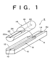
- FIG. 1 there is shown an exploded perspective view of an optical module 2 according to a first preferred embodiment of the present invention.
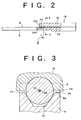
- FIG. 2 is a partially sectional, side view of the optical module 2
- FIG. 3 is a cross section taken along the line 3-3 in FIG. 2.
- the optical module 2 includes a PLC (planar lightwave circuit) 4 and a semicut ferrule assembly 16 connected to the PLC 4.
- the PLC 4 includes a silicon substrate 6 and an optical waveguide layer 8 formed on the silicon substrate 6.
- the optical waveguide layer 8 includes an optical waveguide core 10 and an optical waveguide cladding 12 covering the optical waveguide core 10.
- the optical waveguide core 10 has a square cross section whose side is about 8 ⁇ m.
- An optical signal propagates in the optical waveguide core 10 having a refractive index higher than that of the optical waveguide cladding 12.
- the upper surface of the silicon substrate 6 is exposed at its one end portion 6a, and a V groove 14 is formed on the exposed upper surface 6a of the substrate 6 by anisotropic etching of silicon.
- the position and size of the V groove 14 are set so that when a bare optical fiber having a circular cross section whose diameter is 125 ⁇ m is mounted in the V groove 14, the core (diameter: 9.5 ⁇ m) of the bare optical fiber is aligned with the optical waveguide core 10.
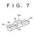
- the semicut ferrule assembly 16 includes a cylindrical ferrule 18 having a through hole 20 and a bare optical fiber 22 inserted and fixed in the through hole 20.
- the ferrule 18 is formed of zirconia, for example.
- the ferrule 18 further includes a flat cut portion 24 for semicylindrically exposing a part of the optical fiber 22 inserted and fixed in the through hole 20.
- the semicut ferrule assembly 16 is fabricated by semicylindrically cutting a part of a completely cylindrical ferrule to thereby form the ferrule 18 having the flat cut portion 24, and next inserting the bare optical fiber 22 into the through hole 20 so that the opposite end faces of the bare optical fiber 22 become substantially flush with the opposite end faces of the ferrule 18.
- the bare optical fiber 22 is fixed by an adhesive in the through hole 20 defined in a cylindrical portion of the ferrule 18 except the flat cut portion 24.
- the semicut ferrule assembly 16 is mounted to the PLC 4 by inserting the bare optical fiber 22 exposed to the flat cut portion 24 into the V groove 14 exposed to the upper surface 6a of the silicon substrate 6 until one end 22a of the bare optical fiber 22 abuts against one end 10a of the optical waveguide core 10, and fixing the flat cut portion 24 of the ferrule 18 to the upper surface 6a of the silicon substrate 6 by using an adhesive.
- a gap 26 is defined between the upper surface 6a of the silicon substrate 6 and the flat cut portion 24 of the ferrule 18.
- the adhesive is applied to this gap 26 to thereby fix the ferrule 18 to the silicon substrate 6.
- Reference numeral 28 in FIG. 3 denotes the core of the bare optical fiber 22. It is shown that the core 28 of the bare optical fiber 22 is aligned with the optical waveguide core 10.
- the optical module 2 according to the first preferred embodiment has the following advantages.
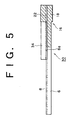
- FIG. 4 there is shown an exploded perspective view of an optical module 30 according to a second preferred embodiment of the present invention.
- FIG. 5 is a partially sectional, side view of the optical module 30, and
- FIG. 6 is a cross section of the optical module 30 as similar to FIG. 3.
- the optical module 30 includes a PLC 4A, a semicut ferrule assembly 16, and a glass plate 34 having a V groove 36.
- the PLC 4A includes a silicon substrate 6 and an optical waveguide layer 8.
- the optical waveguide layer 8 of the PLC 4A includes an optical waveguide core 10 and an optical waveguide cladding 12.
- the optical waveguide cladding 12 is partially removed to form a narrow portion 8a in which the optical waveguide core 10 extends.
- the optical waveguide core 10 extends over the length of the silicon substrate 6.
- the upper surface of the silicon substrate 6 is exposed on the opposite sides of the narrow portion 8a of the optical waveguide layer 8, and a pair of marker grooves 32 for positioning to the glass plate 34 are formed by etching on this exposed upper surface of the silicon substrate 6.
- the semicut ferrule assembly 16 is similar in structure to that of the optical module 2 according to the first preferred embodiment.
- the V groove 36 is formed on the lower surface of the glass plate 34 so as to extend over the length thereof.
- a pair of marker grooves 38 for positioning to the PLC 4A are also formed on the lower surface of the glass plate 34 so as to extend over the length thereof.
- the V groove 36 and the marker grooves 38 are formed by cutting or glass molding, for example.
- the glass plate 34 and the PLC 4A are fixed together by an adhesive in such a manner that the narrow portion 8a of the optical waveguide layer 8 is accommodated in the V groove 36 of the glass plate 34, and that the marker grooves 32 of the PLC 4A are vertically aligned with the marker grooves 38 of the glass plate 34.
- the glass plate 34 and the semicut ferrule assembly 16 are fixed together by an adhesive in such a manner that the bare optical fiber 22 exposed to the flat cut portion 24 of the ferrule 18 is fitted into the V groove 36 of the glass plate 34 to effect self-aligned positioning.
- a gap of about 10 ⁇ m is defined between the flat cut portion 24 of the ferrule assembly 16 and the lower surface of the glass plate 34, and the adhesive is charged into the gap to thereby fix the glass plate 34 and the ferrule assembly 16.
- the shape and size of the V groove 36 and the position of the V groove 36 relative to the marker grooves 32 and 38 are set so that the optical waveguide core 10 is aligned with the core 28 of the bare optical fiber 22, shown in FIG. 6.
- the optical module 30 according to the second preferred embodiment has the following advantages.
- the ferrule assembly 16A includes a cylindrical ferrule 18 having a through hole 20 and a bare optical fiber 22 inserted and fixed in the through hole 20.
- the ferrule 18 has a cylindrical intermediate portion and a pair of flat cut portions 24 formed at the opposite end portions for semicylindrically exposing the opposite end portions of the optical fiber 22.
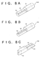
- FIGs. 8A, 8B, and 8C show semicut ferrule assemblies 16B, 16C, and 16D, respectively, according to other preferred embodiments of the present invention.
- the ferrule assembly 16B shown in FIG. 8A is different from the ferrule assembly 16 shown in FIG. 1 in only the point that the width of the flat cut portion 24 is reduced.
- the ferrule assembly 16C shown in FIG. 8B is different from the ferrule assembly 16B shown in FIG. 8A in only the point that the width of the flat cut portion 24 is reduced.
- the ferrule assembly 16D shown in FIG. 8C is different from the ferrule assembly 16 shown in FIG. 1 in only the point that the cylindrical portion of the ferrule 18 is formed at one end thereof with a taper 40.
- the ferrule assembly 16D is effective in configuring a compact wavelength filter module to be hereinafter described.
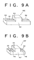
- FIGs. 9A and 9B show semicut ferrule assemblies 16E and 16F, respectively, according to still other preferred embodiments of the present invention.
- the ferrule assembly 16E shown in FIG. 9A is similar to the ferrule assembly 16A shown in FIG. 7 except that a rectangular prismatic ferrule 42 is adopted. That is, the ferrule assembly 16E includes the ferrule 42 having a through hole 44 and a bare optical fiber 22 inserted in the through hole 44.
- the ferrule 42 has a rectangular prismatic intermediate portion and a pair of flat cut portions 46 formed at the opposite end portions for semicylindrically exposing the opposite end portions of the optical fiber 22.
- the ferrule assembly 16F shown in FIG. 9B is similar to the ferrule assembly 16E shown in FIG. 9A except that a plurality of bare optical fibers 22 are inserted and fixed in a plurality of through holes 44 extending through a rectangular prismatic ferrule 42'.
- the outside shape of the ferrule used in the present invention is not necessarily cylindrical for the connection of a PLC and an optical element or the connection of a PLC and another PLC.
- the preferred embodiments shown in FIGs. 9A and 9B intended for size reduction are effective in providing high-density optical connection.
- FIG. 10 there is shown a coupling structure of different types of ferrules.
- a ferrule structure for converting an external size can be simply obtained. This structure is excellent in reliability because no bending of the bare optical fiber 22 occurs.
- the optical module 50 includes a V-grooved PLC 4B, a semicut ferrule assembly 16, and an optical element 52.
- the PLC 4B includes a silicon substrate 6 and an optical waveguide layer 8 formed on an intermediate portion of the silicon substrate 6.
- the ferrule assembly 16 is mounted on one end portion of the silicon substrate 6, and the optical element 52 is mounted on the other end portion of the silicon substrate 6.
- the optical element 52 is a laser diode or a photodiode, for example, and it is mounted on the substrate 6 so as to be optically coupled to the optical waveguide core 10 of the optical waveguide layer 8. Electrodes 54 for the optical element 52 are also formed on the other end portion of the substrate 6.
- the one end portion of the substrate 6 of the PLC 4B is formed with a V groove 14 aligned with the optical waveguide core 10 in the layer 8.
- the flat cut portion 24 of the ferrule assembly 16 is bonded to the one end portion of the substrate 6 so that the bare optical fiber 22 is engaged with the V groove 14 of the substrate 6. Accordingly, the core of the optical fiber 22 is substantially aligned with the optical waveguide core 10, thereby realizing low-loss optical coupling.
- the one end portion of the silicon substrate 6 to which the flat cut portion 24 of the ferrule assembly 16 is bonded is further formed with a plurality of grooves 56 for receiving an adhesive.
- the grooves 56 extend over the width of the substrate 6 in perpendicular relationship to the V groove 14.
- An optical functional circuit such as a wavelength filter, optical branching circuit, optical modulator, and optical switch is incorporated in the optical waveguide layer 8.
- a plurality of optical elements or an optical element array rather than the single optical element 52 may be mounted on the substrate 6.
- a plurality of semicut ferrule assemblies rather than the single semicut ferrule assembly 16 may be mounted on the substrate 6.
- the optical module 58 includes a V-grooved PLC 4C and a pair of semicut ferrule assemblies 16.
- the PLC 4C includes a silicon substrate 6 and an optical waveguide layer 8 formed on an intermediate portion of the silicon substrate 6.
- the pair of ferrule assemblies 16 are mounted on the opposite end portions of the silicon substrate 6.
- the opposite end portions of the substrate 6 of the PLC 4C are formed with a pair of V grooves 14 each aligned with the optical waveguide core 10 in the layer 8.
- the flat cut portions 24 of the ferrule assemblies 16 are bonded to the opposite end portions of the substrate 6 so that the bare optical fibers 22 of the ferrule assemblies 16 are engaged with the V grooves 14 formed on the opposite end portions of the substrate 6. Accordingly, the core of the optical fiber 22 of each ferrule assembly 16 is substantially aligned with the optical waveguide core 10, thereby realizing low-loss optical coupling.
- Each end portion of the silicon substrate 6 to which the flat cut portion 24 of each ferrule assembly 16 is bonded is further formed with a plurality of grooves 56 for receiving an adhesive.
- the grooves 56 formed on each end portion of the substrate 6 extend over the width of the substrate 6 in perpendicular relationship to the V groove 14 formed on the same end portion of the substrate 6.
- An optical functional circuit such as a wavelength filter, optical branching circuit, optical modulator, and optical switch is incorporated in the optical waveguide layer 8.
- the optical module 60 includes a V-grooved silicon substrate 6, a semicut ferrule assembly 16, and an optical element 52.
- the ferrule assembly 16 is mounted on one end portion of the silicon substrate 6, and the optical element 52 is mounted on the other end portion of the silicon substrate 6 so as to be optically coupled to the bare optical fiber 22 of the ferrule assembly 16.
- Electrodes 54 for the optical element 52 are formed on the other end portion of the substrate 6.
- the one end portion of the substrate 6 is formed with a V groove 14 aligned with an active layer of the optical element 52.
- the flat cut portion 24 of the ferrule assembly 16 is bonded to the one end portion of the substrate 6 so that the bare optical fiber 22 is engaged with the V groove 14 of the substrate 6. Accordingly, the core of the optical fiber 22 is substantially aligned with the active layer of the optical element 52, thereby realizing low-loss optical coupling.
- the one end portion of the silicon substrate 6 to which the flat cut portion 24 of the ferrule assembly 16 is bonded is further formed with a plurality of grooves 56 for receiving an adhesive.
- the grooves 56 extend over the width of the substrate 6 in perpendicular relationship to the V groove 14.
- a plurality of optical elements or an optical element array rather than the single optical element 52 may be mounted on the substrate 6.
- the optical module 62 includes a V-grooved silicon substrate 6, a pair of semicut ferrule assemblies 16, and an optical element 52.
- the pair of ferrule assemblies 16 are mounted on the opposite end portions of the silicon substrate 6.
- the optical element 52 is mounted on an intermediate portion of the silicon substrate 6 so as to be sandwiched between the pair of ferrule assemblies 16. Electrodes 54 for the optical element 52 are formed on the intermediate portion of the silicon substrate 6.
- the opposite end portions of the substrate 6 are formed with a pair of V grooves 14 each aligned with an active layer of the optical element 52.
- the flat cut portions 24 of the ferrule assemblies 16 are bonded to the opposite end portions of the substrate 6 so that the bare optical fibers 22 of the ferrule assemblies 16 are engaged with the V grooves 14 formed on the opposite end portions of the substrate 6. Accordingly, the core of the optical fiber 22 of each ferrule assembly 16 is substantially aligned with the active layer of the optical element 52, thereby realizing low-loss optical coupling.
- Each end portion of the silicon substrate 6 to which the flat cut portion 24 of each ferrule assembly 16 is bonded is further formed with a plurality of grooves (not shown) for receiving an adhesive.
- the optical module 64 includes a V-grooved silicon substrate 6, a pair of semicut ferrule assemblies 16, and a thin-film or thin-sheet passive optical component 68.
- the pair of ferrule assemblies 16 are mounted on the opposite end portions of the silicon substrate 6.
- the passive optical component 68 is vertically inserted and fixed in a rectangular groove 66 formed at an intermediate portion of the silicon substrate 6 so as to be sandwiched between the pair of ferrule assemblies 16.
- the rectangular groove 66 extends over the width of the silicon substrate 6.
- the opposite end portions of the substrate 6 are formed with a pair of V grooves 14 aligned with each other.
- the flat cut portions 24 of the ferrule assemblies 16 are bonded to the opposite end portions of the substrate 6 so that the bare optical fibers 22 of the ferrule assemblies 16 are engaged with the V grooves 14 formed on the opposite end portions of the substrate 6. Accordingly, the cores of the optical fibers 22 positioned in the V grooves 14 are substantially aligned with each other, thereby realizing low-loss optical coupling.
- the passive optical component 68 in the form of thin film or thin sheet fixed in the rectangular groove 66 projects from the upper surface of the silicon substrate 6, and the opposite side surfaces of the passive optical component 68 at its projecting portion are sandwiched between the opposite end faces of the ferrule assemblies 16 and bonded thereto. Accordingly, a large bonding area of the passive optical component 68 is ensured, and it is supported from the opposite sides by the ferrule assemblies 16, thereby obtaining a high fixing strength to stabilize the passive optical component 68.
- Each end portion of the silicon substrate 6 to which the flat cut portion 24 of each ferrule assembly 16 is bonded is further formed with a plurality of grooves (not shown) for receiving an adhesive.
- the optical module 70 includes a V-grooved PLC 4D, a pair of semicut ferrule assemblies 16a and 16b, an optical element 52, and a thin-film optical wavelength filter 84.
- the PLC 4D includes a V-grooved silicon substrate 6 and an optical waveguide layer 72 formed on an intermediate portion of the silicon substrate 6.
- the optical waveguide layer 72 is a Y-branch type optical waveguide including a first optical waveguide core 74, a second optical waveguide core 76 connected to an intermediate portion of the first optical waveguide core 74, and an optical waveguide cladding 78 covering the first and second optical waveguide cores 74 and 76.
- the pair of ferrule assemblies 16a and 16b are mounted on one end portion of the silicon substrate 6, and the optical element 52 is mounted on the other end portion of the silicon substrate 6. Electrodes 54 for the optical element 52 are formed on the other end portion of the silicon substrate 6.
- the thin-film optical wavelength filter 84 is vertically inserted and fixed in a rectangular groove 82 cut through the optical waveguide layer 72 into the substrate 6 so as to intersect a Y branch 80 of the Y-branch type optical waveguide, i.e., a junction between the first optical waveguide core 74 and the second optical core 76.
- the rectangular groove 82 extends over the width of the substrate 6.
- the one end portion of the silicon substrate 6 is formed with a pair of V grooves 14 aligned with the first and second optical waveguide cores 74 and 76.
- the flat cut portions 24 of the ferrule assemblies 16a and 16b are bonded to the one end portion of the substrate 6 so that the bare optical fibers 22 of the ferrule assemblies 16a and 16b are engaged with the V grooves 14 formed on the one end portion of the substrate 6. Accordingly, the core of the optical fiber 22 of the ferrule assembly 16a is substantially aligned with the first optical waveguide core 74, and the core of the optical fiber 22 of the ferrule assembly 16b is substantially aligned with the second optical waveguide core 76, thereby realizing low-loss optical coupling.
- the one end portion of the silicon substrate 6 to which the flat cut portions 24 of the ferrule assemblies 16a and 16b are bonded is further formed with a plurality of grooves (not shown) for receiving an adhesive.
- a certain component of light entered the first optical waveguide core 74 from the ferrule assembly 16a is transmitted by the wavelength filter 84 to enter the optical element 52, and the remaining component of the light is reflected by the wavelength filter 84 to enter the second optical waveguide core 76 and to emerge from the ferrule assembly 16b.
- the optical module 86 includes a V-grooved PLC 4E, a pair of semicut ferrule assemblies 16a and 16b, an optical element 52, and a thin-film optical wavelength filter 84.
- the PLC 4E includes a V-grooved silicon substrate 6 and an optical waveguide layer 72 formed on an intermediate portion of the silicon substrate 6.
- the optical waveguide layer 72 has the same structure as that in the eighth preferred embodiment shown in FIG. 16.
- the pair of ferrule assemblies 16a and 16b are mounted on the opposite end portions of the silicon substrate 6, and the optical element 52 is mounted on one end portion of the silicon substrate 6 where the ferrule assembly 16a is mounted. Electrodes 54 for the optical element 52 are formed on the one end portion of the silicon substrate 6.
- the thin-film optical wavelength filter 84 is vertically inserted and fixed in a rectangular groove 82 as similar to the structure in the eighth preferred embodiment shown in FIG. 16.
- the opposite end portions of the silicon substrate 6 are formed with a pair of V grooves 14 aligned with the opposite ends of the first optical waveguide core 74.
- the flat cut portions 24 of the ferrule assemblies 16a and 16b are bonded to the opposite end portions of the substrate 6 so that the bare optical fibers 22 of the ferrule assemblies 16a and 16b are engaged with the V grooves 14 formed on the opposite end portions of the substrate 6. Accordingly, the core of the optical fiber 22 of the ferrule assembly 16a is substantially aligned with the first end of the first optical waveguide core 74, and the core of the optical fiber 22 of the ferrule assembly 16b is substantially aligned with the second end of the first optical waveguide core 74, thereby realizing low-loss optical coupling.
- Each of the opposite end portions of the silicon substrate 6 to which the flat cut portions 24 of the ferrule assemblies 16a and 16b are bonded is further formed with a plurality of grooves (not shown) for receiving an adhesive.
- a certain component of light entered the first optical waveguide core 74 from the ferrule assembly 16a is reflected by the wavelength filter 84 to enter the optical element 52 through the second waveguide core 76, and the remaining component of the light is transmitted by the wavelength filter 84 to enter the ferrule assembly 16b and to emerge therefrom.
- the optical element 52 is a light emitting element such as a laser diode
- a certain component of light emitted from the optical element 52 is reflected by the wavelength filter 84 to enter the ferrule assembly 16a and to emerge therefrom, and the remaining component of the light is transmitted by the wavelength filter 84 to enter the ferrule assembly 16b and to emerge therefrom.
- the optical module 88 includes a V-grooved PLC 4F, a semicut ferrule assembly 16, a pair of optical elements 52a and 52b, and a thin-film optical wavelength filter 84.
- the PLC 4F includes a V-grooved silicon substrate 6 and an optical waveguide layer 72 formed on an intermediate portion of the silicon substrate 6.
- the optical waveguide layer 72 has the same structure as that in the eighth preferred embodiment shown in FIG. 16.
- the ferrule assembly 16 and the optical element 52a are mounted on one end portion of the silicon substrate 6, and the optical element 52b is mounted on the other end portion of the silicon substrate 6. Electrodes 54 for the optical element 52a are formed on the one end portion of the silicon substrate 6, and electrodes 54 for the optical element 52b are formed on the other end portion of the silicon substrate 6.
- the thin-film optical wavelength filter 84 is vertically inserted and fixed in a rectangular groove 82 as similar to the structure in the eighth preferred embodiment shown in FIG. 16.
- the wavelength filter 84 transmits light having wavelengths in a 1.55 ⁇ m band, and reflects light having wavelengths in a 1.3 ⁇ m band.
- the one end portion of the silicon substrate 6 is formed with a V groove 14 aligned with the first end of the first optical waveguide core 74.
- the flat cut portion 24 of the ferrule assembly 16 is bonded to the one end portion of the substrate 6 so that the bare optical fiber 22 of the ferrule assembly 16 is engaged with the V groove 14 formed on the one end portion of the substrate 6. Accordingly, the core of the optical fiber 22 of the ferrule assembly 16 is substantially aligned with the first end of the first optical waveguide core 74, thereby realizing low-loss optical coupling.
- the one end portion of the silicon substrate 6 to which the flat cut portion 24 of the ferrule assembly 16 is bonded is further formed with a plurality of grooves (not shown) for receiving an adhesive.
- a certain component of light entered the first optical waveguide core 74 from the ferrule assembly 16 is reflected by the wavelength filter 84 to enter the optical element 52a, and the remaining component of the light is transmitted by the wavelength filter 84 to enter the optical element 52b.
- the optical element 52a is a light emitting element such as a laser diode
- a certain component of light emitted from the optical element 52a is reflected by the wavelength filter 84 to enter the ferrule assembly 16 and to emerge therefrom, and the remaining component of the light is transmitted by the wavelength filter 84 to enter the optical element 52b.
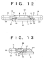
- FIG. 19 there is shown a perspective view of an optical module 90 according to an eleventh preferred embodiment of the present invention.
- the optical module 90 includes a V-grooved silicon substrate 6, a semicut ferrule assembly 16A similar to that shown in FIG. 7, and an optical element 52.
- the silicon substrate 6 is formed at its one end portion with a V groove 14.
- the ferrule assembly 16A is mounted on the silicon substrate 6 in such a manner that one of the two cut flat portions 24 of the ferrule assembly 16A is bonded to the one end portion of the substrate 6 in the condition where the bare optical fiber 22 is engaged with the V groove 14.
- a PLC not shown
- an optical functional system can be simply configured.
- FIG. 20 there is shown a perspective view of an optical module 92 according to a twelfth preferred embodiment of the present invention.
- the optical module 92 is configured by connecting two optical modules each similar to the optical module 90 shown in FIG. 19 to a PLC 4G at one end portion thereof.
- a semicut ferrule assembly 16 is mounted on the other end portion of the PLC 4G.
- a wavelength filter or an optical switch circuit may be mounted in the optical waveguide layer 8 of the PLC 4G.
- the optical module 94 includes a V-grooved silicon substrate 6, a bare optical fiber 22, and an optical element 52.
- a V groove 14 is formed on the upper surface of the silicon substrate 6 at one end portion thereof by anisotropic etching of silicon.
- the bare optical fiber 22 is fitted in the V groove 14 of the substrate 6, and the optical element 52 is mounted on the upper surface of the substrate 6 so as to be substantially aligned with the core of the optical fiber 22.
- the size of the V groove 14 is set so that the core of the optical fiber 22 fitted in the V groove 14 is optically coupled to the optical element 52.
- a rectangular groove 96 perpendicular to the V groove 14 is formed by cutting on the upper surface of the substrate 6, so as to eliminate a slant portion formed at one end of the V groove 14 opposed to the optical element 52.
- the optical module 98 includes a V-grooved silicon substrate 6, a pair of bare optical fibers 22, and an optical element 52'.
- a pair of V grooves 14 aligned with each other are formed on the upper surface of the silicon substrate 6 at its opposite end portions.
- the bare optical fibers 22 are fitted in the V grooves 14 of the substrate 6, and the optical element 52' is mounted on the upper surface of the substrate 6 at its intermediate portion so as to be substantially aligned with the cores of the optical fibers 22.
- the size of each V groove 14 is set so that the cores of the optical fibers 22 are optically coupled to the optical element 52'.
- a pair of rectangular grooves 96 for the V grooves 14 are formed on the upper surface of the substrate 6 as similarly to the preferred embodiment shown in FIG. 21.
- the optical element 52' is an LD amplifier which amplifies an optical signal.
- FIG. 22B shows an optical module 100 as a modification of the preferred embodiment shown in FIG. 22A.
- the optical module 100 differs from the optical module 98 shown in FIG. 22A in only the point that two pairs of bare optical fibers 22 are fitted in two pairs of V grooves 14, and that a pair of optical elements 52' are mounted on the silicon substrate 6.
- the optical module 102 includes a silicon substrate 6 having a V groove 14, a semicut ferrule assembly 16D having a taper 40 similar to that shown in FIG. 8C, and an optical element 52.
- the semicut ferrule assembly 16D is mounted on the silicon substrate 6 so that the optical fiber 22 of the ferrule assembly 16D is fitted in the V groove 14 of the substrate 6, and the optical element 52 is mounted on the substrate 6 so as to be optically coupled to the core of the optical fiber 22 fitted in the V groove 14.
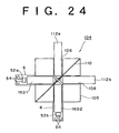
- the optical module 104 includes a substrate 105, two cylindrical ferrule assemblies 112a and 112b, two semicut ferrule assemblies 16D1 and 16D2, two optical elements 52a and 52b, and a wavelength filter 110.
- Two grooves 106 and 108 orthogonal to each other are formed on the upper surface of the substrate 105.
- the cylindrical ferrule assemblies 112a and 112b each having a tapered front end are inserted in the grooves 106 and 108, respectively.
- the semicut ferrule assemblies 16D1 and 16D2 each having a tapered front end are inserted in the grooves 108 and 106, respectively.
- the ferrule assemblies 112a and 16D2 are inserted in the groove 106 in such a manner that their respective tapered front ends are opposed to each other
- the ferrule assemblies 112b and 16D1 are inserted in the groove 108 in such a manner that their respective tapered front ends are opposed to each other.
- optical fibers are inserted and fixed in the through holes of the ferrule assemblies 112a, 112b, 16D1, and 16D2.
- the wavelength filter 110 is inserted and fixed in a groove formed on the upper surface of the substrate 105 so as to be inclined 45° with respect to the grooves 106 and 108.
- the optical elements 52a and 52b are mounted on silicon substrates 6 on which the ferrule assemblies 16D1 and 16D2 are mounted.
- Incident light from the cylindrical ferrule assembly 112a is transmitted and reflected by the wavelength filter 110, wherein a transmitted component of the light enters the optical element 52b through the ferrule assembly 16D2 and a reflected component of the light enters the optical element 52a through the ferrule assembly 16D1.
- incident light from the cylindrical ferrule assembly 112b is also transmitted and reflected by the wavelength filter 110, wherein a transmitted component of the light enters the optical element 52a through the ferrule assembly 16D1 and a reflected component of the light enters the optical element 52b through the ferrule assembly 16D2.
- the optical element 52a is a light emitting element and the optical element 52b is a photodetecting element
- a bidirectional wavelength division multiplexing optical transmission module can be simply fabricated, and the module can be reduced in size.
- the optical module 114 includes a substrate 116, an LD amplifier array 118, a pair of semicut ferrule assemblies 16F', a pair of PLCs 4H and 4H', and a plurality of semicut ferrule assemblies 16.
- the LD amplifier array 118 is mounted on the substrate 116.
- the semicut ferrule assemblies 16F' are mounted on the substrate 116 with the LD amplifier array 118 interposed therebetween.
- Each ferrule assembly 16F' is similar to the ferrule assembly 16F shown in FIG. 9B.
- the ferrule assemblies 16F' are mounted also on the substrates 6 of the PLCs 4H and 4H'.
- the LD amplifier array 118 is optically connected through the ferrule assemblies 16F' to the PLCs 4H and 4H'.
- the semicut ferrule assemblies 16 are mounted on the substrate 6 of each of the PLCs 4H and 4H' so as to be optically connected to the optical waveguide layer 8 of each of the PLCs 4H and 4H'.
- optical signals input through the left ferrule assemblies 16 into the PLC 4H are amplified by the LD amplifier array 118, and amplified optical signals from the LD amplifier array 118 are input into the PLC 4H' and output from the right ferrule assemblies 16.
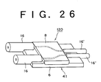
- the optical module 120 includes a V-grooved PLC 4I, a plurality of semicut ferrule assemblies 16 each having a larger diameter, and a plurality of semicut ferrule assemblies 16' each having a smaller diameter.
- the ferrule assemblies 16 are mounted on one end portion of the substrate 6 of the PLC 4I, and the ferrule assemblies 16' are mounted on the other end portion of the substrate 6.
- the ferrule assemblies 16 are arranged with a pitch larger than that of the ferrule assemblies 16'. Thus, the external size and pitch of plural ferrule assemblies can be freely changed.
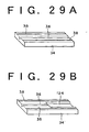
- FIG. 28 shows a PLC 4J used in the nineteenth preferred embodiment
- FIG. 29A is a glass plate 34 used in the nineteenth preferred embodiment.
- the PLC 4J includes a silicon substrate 6 and an optical waveguide layer 8 formed on the silicon substrate 6.
- the optical waveguide layer 8 has a pair of narrow portions 8a and 8b at the opposite end portions formed by partially cutting the cladding region.
- a pair of marker grooves 32 for positioning to the glass plate 34 are formed on the opposite sides of the narrow waveguide portion 8a on the upper surface of the substrate 6, and a pair of marker grooves 33 for positioning to another member (not shown) are formed on the opposite sides of the narrow waveguide portion 8b on the upper surface of the substrate 6.
- the substrate 6 has no V groove in this preferred embodiment.
- the glass plate 34 has a V groove 36 formed by cutting or the like and a pair of marker grooves 38 formed by cutting or the like on the opposite sides of the V groove 36.
- the PLC 4J and the glass plate 34 are bonded together with a high dimensional accuracy by a passive alignment technique in such a manner that the marker grooves 32 of the PLC 4J are vertically aligned with the marker grooves 38 of the glass plate 34, and that the narrow waveguide portion 8a of the PLC 4J is accommodated in the V groove 36 of the glass plate 34.
- the glass plate 34 and the semicut ferrule assembly 16 are bonded together in such a manner that the bare optical fiber 22 of the ferrule assembly 16 is fitted in the V groove 36 of the glass plate 34 to effect positioning by a self alignment technique, and that the flat cut portion 24 of the ferrule assembly 16 is bonded to the glass plate 34.
- the PLC 4J has no V groove, high-precision optical coupling between the bare optical fiber 22 of the ferrule assembly 16 and the optical waveguide core of the PLC 4J can be relatively simply obtained by using the V-grooved glass plate 34.
- FIG. 30A there is shown an exploded perspective view of an optical module 126 according to a twentieth preferred embodiment of the present invention.
- FIG. 30B is a perspective view of the optical module 126 in its assembled condition.
- the optical module 126 includes a V-grooved PLC 4K and a multifiber semicut connector 128.
- the PLC 4K includes a silicon substrate 6 and an optical waveguide layer 8 formed on the silicon substrate 6.
- the optical waveguide layer 8 includes a Y-branched optical waveguide core 10 and an optical waveguide cladding 12 covering the core 10.
- the Y-branched optical waveguide core 10 consists of a first core portion 10a and a second core portion 10b connected to an intermediate portion of the first core portion 10a.
- An optical signal propagates in the optical waveguide core 10 having a refractive index higher than that of the optical waveguide cladding 12.
- the silicon substrate 6 has an exposed surface 6a formed with two V grooves 14 respectively aligned with the first and second core portions 10a and 10b.
- the multifiber semicut connector 128 has two bare optical fibers 22 optically coupled to the first and second core portions 10a and 10b.
- the position and size of the V grooves 14 are set so that when the bare optical fibers 22 are fitted in the V grooves 14, the cores of the optical fibers 22 are substantially aligned with the first and second core portions 10a and 10b of the Y-branched optical waveguide core 10.
- the multifiber semicut connector 128 includes a block 130 having two through holes in which the two optical fibers 22 are inserted and fixed.
- the block 130 has a flat cut portion 132 for semicylindrically exposing the optical fibers 22.
- the block 130 having the flat cut portion 132 is formed by transfer molding of plastic using a mold.
- the bare optical fibers 22 are inserted in the through holes of the block 130 and bonded thereto at its portion except the flat cut portion 132.
- a pair of guide pins 134 are inserted and fixed in other through holes formed in the block 130. The insertion and fixing of the guide pins 134 may be carried out after connecting the PLC 4K to the multifiber semicut connector 128.
- the PLC 4K is bonded at the exposed surface 6a to the flat cut portion 132 of the multifiber semicut connector 128 so that the optical fibers 22 of the connector 128 are fitted in the V grooves 14 of the PLC 4K. Accordingly, the cores of the optical fibers 22 are substantially aligned with the first and second core portions 10a and 10b of the Y-branched optical waveguide core 10, thereby realizing low-loss optical coupling.
- the exposed surface 6a of the silicon substrate 6 of the PLC 4K to which the flat cut portion 132 of the connector 128 is bonded is further formed with a plurality of grooves 56 for receiving an adhesive.
- the optical module 126 can solve the problems in the conventional receptacle structure, and has the following advantages.
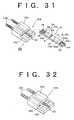
- FIG. 31 there is shown an exploded perspective view of an optical module 136 according to a twenty-first preferred embodiment of the present invention.
- the optical module 136 differs from the optical module 126 shown in FIG. 30A in only the structure of a PLC 4L.
- the PLC 4L includes a V-grooved silicon substrate 6 having exposed surfaces 6a and 6b at the opposite end portions, and an optical waveguide layer 8 formed on an intermediate portion of the silicon substrate 6.
- Two V grooves 14 are formed on the exposed surface 6a of the substrate 6, and three optical elements 52a, 52b, and 52c are mounted on the exposed surface 6b of the substrate 6.
- the optical waveguide layer 8 includes a Y-branched optical waveguide core 10 and an optical waveguide cladding 12 covering the core 10.
- the optical waveguide core 10 includes first and second core portions 10a and 10b respectively aligned with the two V grooves 14, and third and fourth core portions 10c and 10d respectively aligned with the optical elements 52a and 52b.
- the optical element 52a is a laser diode
- the optical element 52b is a photodiode for detection of an optical signal
- the optical element 52c is a photodiode for monitoring of light.
- Reference numerals 54 are electrodes for the optical elements 52a, 52b, and 52c.
- FIG. 32 there is shown a perspective view of a multifiber semicut connector 138 according to another preferred embodiment.
- the multifiber semicut connector 138 differs from the connector 128 shown in FIG. 30A in only the point that a groove 140 is additionally formed.
- the groove 140 is formed on the flat cut portion 132 near the boundary between the exposed part of the optical fibers 22 and the unexposed part of the optical fibers 22 so as to extend in a direction perpendicular to the optical fibers 22.
- the groove 140 has a width of 0.1 to 1 mm, for example, and is slightly lowered from the horizontal upper surface of the flat cut portion 132.
- the groove 140 functions to receive the adhesive leaked from the through holes, thereby preventing the adhesive from sticking to the horizontal surface of the flat cut portion 132 where the exposed part of the optical fibers 22 is placed.
- the optical module 142 includes a multifiber semicut connector 128' and a PLC 4K'.
- the multifiber semicut connector 128' is similar to the connector 128 shown in FIG. 30A except that the bare optical fibers 22 of the connector 128' project from the block 130 by about 0.1 to 2 mm.
- the PLC 4K' is similar to the PLC 4K shown in FIG. 30A except that the exposed surface 6a of the PLC 4K' is longer than that of the PLC 4K.
- the optical module 144 includes a semicut ferrule assembly 16F similar to that shown in FIG. 9B, a PLC 4K similar to that shown in FIG. 30A, a substrate 146 having two V grooves 148, and two optical elements 52 mounted on the substrate 146.
- the two optical elements 52 are aligned with the two V grooves 148, respectively.
- a plurality of grooves 150 for receiving an adhesive are also formed on the substrate 146.
- the grooves 150 extend over the width of the substrate 146 in perpendicular relationship to the V grooves 148.
- the PLC 4K is bonded to the flat cut portion 46 formed at one end portion of the ferrule assembly 16F so that an exposed part of the optical fibers 22 of the ferrule assembly 16F is fitted in the V grooves 14 of the PLC 4K.
- the substrate 146 is bonded to the other flat cut portion 46 of the ferrule assembly 16F so that the other exposed part of the optical fibers 22 of the ferrule assembly 16F is fitted in the V grooves 148 of the substrate 146.
- the optical elements 52 mounted on the substrate 146 are optically coupled through the ferrule assembly 16F to the PLC 4K.
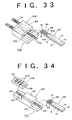
- FIG. 35A there is shown an exploded perspective view of an optical module 152 according to a twenty-fourth preferred embodiment of the present invention.
- FIG. 35B is a perspective view of the optical module 152 in its assembled condition.
- the optical module 152 includes a V-grooved PLC 4M and two multifiber semicut connectors 126' and 154 optically coupled to each other through the PLC 4M.
- the PLC 4M includes a silicon substrate 6 and an optical waveguide layer 8 formed on an intermediate portion of the substrate 6.
- the substrate 6 has an exposed surface 6a at one end portion and another exposed surface 6b at the other end portion.
- the exposed surface 6a is formed with two V grooves 14, and the exposed surface 6b is formed with at least four V grooves 14.
- the optical waveguide layer 8 includes two Y-branch type (1 ⁇ N branch type where N is an integer greater than 1) optical waveguide cores 10 and an optical waveguide cladding 12 covering the cores 10.
- Each optical waveguide core 10 has one end aligned to one of the V grooves 14 formed on the exposed surface 6a and has N ends aligned to N of the V grooves 14 formed on the exposed surface 6b.
- the flat cut portion 132 of the connector 126' is bonded to the exposed surface 6a of the PLC 4M so that the optical fibers 22 of the connector 126' are fitted in the V grooves 14 formed on the exposed surface 6a.
- the flat cut portion 132 of the connector 154 is bonded to the exposed surface 6b of the PLC 4M so that the optical fibers 22 of the connector 154 are fitted in the V grooves 14 formed on the exposed surface 6b.
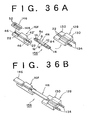
- FIG. 36A there is shown an exploded perspective view of an optical module 156 according to a twenty-fifth preferred embodiment of the present invention.
- FIG. 36B is a perspective view of the optical module 156 in its assembled condition.
- the optical module 156 is similar to the optical module 144 shown in FIG. 34 with the exception that a multifiber semicut connector 128 is added. That is, the optical module 156 includes a PLC 4N, a semicut ferrule assembly 16F, a substrate 146, and the multifiber semicut connector 128.
- the PLC 4N includes a V-grooved silicon substrate 6 and an optical waveguide layer 8 formed on an intermediate portion of the silicon substrate 6.
- the silicon substrate 6 has exposed surfaces 6a and 6b at the opposite end portions.
- the optical waveguide layer 8 includes a Y-branch type optical waveguide core 10 and an optical waveguide cladding 12 covering the core 10 as similar to the structure of the PLC 4L shown in FIG. 31.
- a wavelength filter 84 is mounted on the optical waveguide layer 8.
- the PLC 4N is bonded at the exposed surface 6a to the flat cut portion 46 of the ferrule assembly 16F at its one end portion so that the optical fibers 22 exposed to this portion of the ferrule assembly 16F are fitted in the V grooves 14 formed on the exposed surface 6a of the PLC 4N.
- the substrate 146 is bonded to the flat cut portion 46 of the ferrule assembly 16F at its other end portion so that the optical fibers 22 exposed to this portion of the ferrule assembly 16F are fitted in the V grooves 148 of the substrate 146.
- the multifiber semicut connector 128 is similar to that shown in FIG. 31.
- the connector 128 is bonded at the flat cut portion 132 to the exposed surface 6b of the PLC 4N so that the optical fibers 22 exposed to the flat cut portion 132 are fitted in the V grooves 14 formed on the exposed surface 6b.
- the optical elements 52 mounted on the substrate 146 can be optically coupled through the ferrule assembly 16F and the PLC 4N to the connector 128.
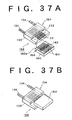
- FIG. 37A there is shown an exploded perspective view of an optical module 158 according to a twenty-sixth preferred embodiment of the present invention.
- FIG. 37B is a perspective view of the optical module 158 in its assembled condition.
- the optical module 158 includes a V-grooved substrate 160, an optical element array 162 mounted on the substrate 160, and a multifiber semicut connector 154 similar to that shown in FIG. 35A.
- the optical element array 162 is an LD array or a PD array, for example.
- a plurality of electrodes 164 for the optical element array 162 are formed on the substrate 160.
- the substrate 160 has a mount surface 160a formed with a plurality of V grooves 166 respectively corresponding to a plurality of individual optical elements constituting the optical element array 162.
- the substrate 160 is bonded at the mount surface 160a to the flat cut portion 132 of the connector 154 so that the optical fibers 22 of the connector 154 are fitted in the V grooves 166 of the substrate 160. With this configuration, the individual optical elements of the optical element array 162 are optically coupled to the optical fibers 22, respectively.
- FIG. 38 there is shown an exploded perspective view of an optical module 168 according to a twenty-seventh preferred embodiment of the present invention.
- the optical module 168 is similar to the optical module 126 shown in FIG. 30A except that a multifiber semicut connector 128' is used in place of the connector 128.
- the multifiber semicut connector 128' includes a silicon substrate 170 having two V grooves 172 and two V grooves 174, two optical fibers 22 fitted in the two V grooves 172, two guide pins 134 fitted in the two V grooves 174, and a cover 176 fixed to the silicon substrate 170 for partially covering the optical fibers 22 and the guide pins 134.
- the silicon substrate 170 has an exposed surface 170a for semicylindrically exposing the optical fibers 22.
- the cover 176 also has two V grooves respectively opposed to the two V grooves 172 for the optical fibers 22 and two V grooves respectively opposed to the two V grooves 174 for the guide pins 134.
- the PLC 4K is bonded at the exposed surface 6a to the exposed surface 170a of the substrate 170 so that the optical fibers 22 are fitted in the V grooves 14 of the PLC 4K.
- FIG. 39A there is shown an exploded perspective view of an optical module 178 according to a twenty-eighth preferred embodiment of the present invention.
- FIG. 39B is a perspective view of the optical module 178 in its assembled condition.
- the optical module 178 includes a PLC 4P, a multifiber semicut connector 128 similar to that shown in FIG. 30A, and a V-grooved glass plate 182.
- the PLC 4P includes a silicon substrate 6 and an optical waveguide layer 8 formed on the silicon substrate 6.
- the optical waveguide layer 8 includes a Y-branched optical waveguide core 10 and an optical waveguide cladding 12 covering the core 10.
- the Y-branched optical waveguide core 10 consists of a first core portion 10a and a second core portion 10b connected to an intermediate portion of the first core portion 10a.
- the cladding 12 is partially removed at one end portion of the layer 8 to form a narrow waveguide portion 8a.
- the narrow waveguide portion 8a includes the first and second core portions 10a and 10b. Accordingly, the silicon substrate 6 has two exposed surfaces 6a on the opposite sides of the narrow waveguide portion 8a. A pair of marker grooves 180 are formed on the exposed surfaces 6a of the substrate 6.
- the glass plate 182 is formed with two V grooves 184 for receiving the optical fibers 22 of the connector 128, a relatively wide groove 186 for receiving the narrow waveguide portion 8a of the optical waveguide layer 8 of the PLC 4P, and a pair of marker grooves 188 to be vertically aligned with the pair of marker grooves 180 of the PLC 4P.
- the PLC 4P is bonded at the exposed surfaces 6a to the glass plate 182 so that the narrow waveguide portion 8a of the PLC 4P is accommodated in the groove 186 of the glass plate 182 and that the marker grooves 180 of the PLC 4P are vertically aligned with the marker grooves 188 of the glass plate 182, thereby positioning and fixing the PLC 4P and the glass plate 182 with a high dimensional accuracy by a passive alignment technique.
- the glass plate 182 is bonded to the flat cut portion 132 of the connector 128 so that the optical fibers 22 of the connector 128 are fitted in the V grooves 184 of the glass plate 182 to thereby position the glass plate 182 to the connector 128.
- the PLC 4P has no V grooves, high-precision optical coupling between the bare optical fibers 22 of the connector 128 and the first and second core portions 10a and 10b of the optical waveguide core 10 of the PLC 4P can be realized relatively simply by using the V-grooved glass plate 182.
- a receptacle type optical module suitable for cost reduction and size reduction by using a semicut ferrule assembly at an interface to an optical fiber.
Landscapes
- Physics & Mathematics (AREA)
- General Physics & Mathematics (AREA)
- Optics & Photonics (AREA)
- Optical Couplings Of Light Guides (AREA)
- Mechanical Coupling Of Light Guides (AREA)
Applications Claiming Priority (2)
| Application Number | Priority Date | Filing Date | Title |
|---|---|---|---|
| JP35053598 | 1998-12-09 | ||
| JP35053598A JP3850569B2 (ja) | 1998-12-09 | 1998-12-09 | フェルールアセンブリ及び光モジュール |
Publications (3)
| Publication Number | Publication Date |
|---|---|
| EP1008879A2 true EP1008879A2 (fr) | 2000-06-14 |
| EP1008879A3 EP1008879A3 (fr) | 2004-08-18 |
| EP1008879B1 EP1008879B1 (fr) | 2011-04-20 |
Family
ID=18411155
Family Applications (1)
| Application Number | Title | Priority Date | Filing Date |
|---|---|---|---|
| EP99113623A Expired - Lifetime EP1008879B1 (fr) | 1998-12-09 | 1999-07-12 | Assemblage d'embout et module optique |
Country Status (4)
| Country | Link |
|---|---|
| US (6) | US6241399B1 (fr) |
| EP (1) | EP1008879B1 (fr) |
| JP (1) | JP3850569B2 (fr) |
| DE (1) | DE69943370D1 (fr) |
Cited By (5)
| Publication number | Priority date | Publication date | Assignee | Title |
|---|---|---|---|---|
| WO2002039168A1 (fr) * | 2000-11-07 | 2002-05-16 | Zenastra Photonics Inc. | Procede pour preparer les fibres optiques a la connexion a d'autres fibres ou a des guides d'ondes planaires ainsi qu'un dispositif destine a cette connexion |
| FR2821933A1 (fr) * | 2001-03-07 | 2002-09-13 | Teem Photonics | Element de maintien et d'indexation d'une structure guidante asymetrique, et son utilisation pour la connexion de la structure a un composant d'optique integree |
| FR2822249A1 (fr) * | 2001-03-16 | 2002-09-20 | Teem Photonics | Structure apte a connecter optiquement un composant optique fibre et un composant optique non fibre et procede de mise en oeuvre de la structure pour realiser la connexion |
| EP1229365A3 (fr) * | 2001-01-16 | 2005-01-19 | Molex Incorporated | Connection par alignement passif pour fibres optiques |
| EP1434066B1 (fr) * | 2001-10-04 | 2012-04-11 | Panasonic Corporation | Module de filtre optique |
Families Citing this family (62)
| Publication number | Priority date | Publication date | Assignee | Title |
|---|---|---|---|---|
| JP2001108847A (ja) * | 1999-10-07 | 2001-04-20 | Mitsubishi Electric Corp | 光モジュール |
| US6848839B2 (en) * | 2000-04-07 | 2005-02-01 | Shipley Company, L.L.C. | Methods and devices for coupling optoelectronic packages |
| US6866426B1 (en) | 2000-04-07 | 2005-03-15 | Shipley Company, L.L.C. | Open face optical fiber array for coupling to integrated optic waveguides and optoelectronic submounts |
| US6788853B2 (en) * | 2000-06-28 | 2004-09-07 | Shipley Company, L.L.C. | Method for cleaving integrated optic waveguides to provide a smooth waveguide endface |
| US6707970B2 (en) | 2000-12-15 | 2004-03-16 | Intel Corporation | Alignment of fiber optic bundle to array waveguide using an epoxy |
| US6886989B2 (en) | 2000-12-15 | 2005-05-03 | Intel Corporation | Alignment of fiber optic bundle to array waveguide using pins |
| US6628865B2 (en) * | 2000-12-15 | 2003-09-30 | Intel Corporation | Alignment of optical fibers to an etched array waveguide |
| SE521455C2 (sv) * | 2001-07-05 | 2003-11-04 | Ericsson Telefon Ab L M | Anslutningsenhet för optiska fibrer samt fiberferrulmodul |
| GB2379995B (en) * | 2001-09-21 | 2005-02-02 | Kamelian Ltd | An optical coupling |
| US6860642B2 (en) | 2002-03-14 | 2005-03-01 | Intel Corporation | Compact optical package with modular optical connector |
| US6869230B2 (en) * | 2002-07-02 | 2005-03-22 | Sae Magnetics (Hong Kong) | Assembly for high-speed optical transmitter or receiver |
| JP3994839B2 (ja) * | 2002-09-25 | 2007-10-24 | 住友電気工業株式会社 | 光モジュール |
| US7376312B2 (en) * | 2002-11-05 | 2008-05-20 | Rohm Co., Ltd. | Optical module and method for manufacturing the same |
| US7076136B1 (en) * | 2003-03-11 | 2006-07-11 | Inplane Photonics, Inc. | Method of attaching optical fibers to integrated optic chips that excludes all adhesive from the optical path |
| US6883978B2 (en) * | 2003-06-26 | 2005-04-26 | Matsushita Electric Industrial Co., Ltd. | Low cost package design for fiber coupled optical component |
| US7284913B2 (en) | 2003-07-14 | 2007-10-23 | Matsushita Electric Industrial Co., Ltd. | Integrated fiber attach pad for optical package |
| JP4016913B2 (ja) | 2003-08-28 | 2007-12-05 | 住友電気工業株式会社 | 光モジュール及び光モジュール組立方法 |
| US7410088B2 (en) * | 2003-09-05 | 2008-08-12 | Matsushita Electric Industrial, Co., Ltd. | Solder preform for low heat stress laser solder attachment |
| US7021838B2 (en) | 2003-12-16 | 2006-04-04 | Matsushita Electric Industrial Co., Ltd. | Optimizing alignment of an optical fiber to an optical output port |
| JP2005181959A (ja) * | 2003-12-22 | 2005-07-07 | Rohm & Haas Electronic Materials Llc | 光ファイバーをプリント配線板の埋め込み型導波路に連結する方法および構造体 |
| JP4269979B2 (ja) * | 2004-03-04 | 2009-05-27 | 日立電線株式会社 | 波長多重光送信モジュール |
| JP2005352453A (ja) * | 2004-05-12 | 2005-12-22 | Nec Corp | 光ファイバ部品及び光導波路モジュール並びにこれらの製造方法 |
| KR20090130153A (ko) * | 2004-06-16 | 2009-12-17 | 히다치 가세고교 가부시끼가이샤 | 광도파로구조체, 광도파로형 광모듈 및 광파이버 어레이 |
| US20050282413A1 (en) * | 2004-06-21 | 2005-12-22 | Israel Frederick S | Small form factor pluggable module providing passive optical signal processing of wavelength division multiplexed signals |
| ATE492828T1 (de) * | 2004-06-25 | 2011-01-15 | Andrea Pizzarulli | Verfahren zum zusammenbau optoelektonischer baugruppen und optoelektronische baugruppe |
| US7177504B2 (en) * | 2004-09-30 | 2007-02-13 | Intel Corporation | Manufacturable connectorization process for optical chip-to-chip interconnects |
| US7263260B2 (en) * | 2005-03-14 | 2007-08-28 | Matsushita Electric Industrial Co., Ltd. | Low cost, high precision multi-point optical component attachment |
| WO2006113810A2 (fr) | 2005-04-19 | 2006-10-26 | Adc Telecommunications, Inc. | Sortie de fibre a connecteur integre |
| US7288438B2 (en) * | 2005-04-28 | 2007-10-30 | Intel Corporation | Solder deposition on wafer backside for thin-die thermal interface material |
| JP2007271998A (ja) * | 2006-03-31 | 2007-10-18 | Nec Corp | 光コネクタ及び光モジュール |
| JP4749317B2 (ja) * | 2006-12-19 | 2011-08-17 | 株式会社フジクラ | 光路変換型光コネクタ及びこれを用いた回路基板 |
| JP5156502B2 (ja) * | 2007-06-26 | 2013-03-06 | パナソニック株式会社 | 光モジュール |
| US20090326525A1 (en) * | 2008-06-26 | 2009-12-31 | Jessica Hixon | Laser fiber capillary apparatus and method |
| JP4889695B2 (ja) * | 2008-08-07 | 2012-03-07 | 日東電工株式会社 | 光導波路の組み合わせ構造体 |
| US8200056B2 (en) * | 2008-10-16 | 2012-06-12 | Lightwire LLC | Multi-fiber interface to photonic subassembly |
| WO2011044090A2 (fr) * | 2009-10-09 | 2011-04-14 | Corning Incorporated | Composants, sous-assemblages et assemblages de câbles optiques actifs à photonique intégrée sur silicium |
| US8915659B2 (en) | 2010-05-14 | 2014-12-23 | Adc Telecommunications, Inc. | Splice enclosure arrangement for fiber optic cables |
| KR101176950B1 (ko) * | 2010-09-17 | 2012-08-30 | 주식회사 유나이브 | 부품의 수동 정렬을 구현하는 광 송수신 장치 및 부품의 수동 정렬방법 |
| JP5254296B2 (ja) * | 2010-09-24 | 2013-08-07 | 日本電信電話株式会社 | キャピラリ |
| US8885998B2 (en) | 2010-12-09 | 2014-11-11 | Adc Telecommunications, Inc. | Splice enclosure arrangement for fiber optic cables |
| JP2012163614A (ja) * | 2011-02-03 | 2012-08-30 | Furukawa Electric Co Ltd:The | Soa−plcハイブリッド集積偏波ダイバーシティ回路およびその製造方法 |
| TWI494626B (zh) * | 2011-04-01 | 2015-08-01 | Hon Hai Prec Ind Co Ltd | 光纖耦合連接器 |
| US8534928B2 (en) * | 2011-11-28 | 2013-09-17 | Corning Cable Systems Llc | Optical fiber assemblies, optical fiber organizers and methods of fabricating optical fiber assemblies |
| US8876410B2 (en) | 2012-01-11 | 2014-11-04 | Cisco Technology, Inc. | Self-aligning connectorized fiber array assembly |
| GB2522381B (en) * | 2012-12-04 | 2018-06-13 | Univ Southampton | Apparatus comprising at least one optical device optically coupled to at least one waveguide on an optical chip |
| JP6021619B2 (ja) * | 2012-12-05 | 2016-11-09 | 富士通コンポーネント株式会社 | 光コネクタ、光コネクタシステム、光バックプレーン装置 |
| US9243784B2 (en) | 2012-12-20 | 2016-01-26 | International Business Machines Corporation | Semiconductor photonic package |
| US9400356B2 (en) * | 2013-03-14 | 2016-07-26 | International Business Machines Corporation | Fiber pigtail with integrated lid |
| JP2014182202A (ja) * | 2013-03-18 | 2014-09-29 | Fujitsu Ltd | 電子機器および光コネクタ |
| JPWO2015098854A1 (ja) * | 2013-12-27 | 2017-03-23 | 株式会社フジクラ | 光学装置の製造方法 |
| US9651745B2 (en) * | 2014-09-25 | 2017-05-16 | Optomedia Technology Inc | Optical connector module for aligning optical connectors to optical connecting seat |
| US9423561B1 (en) * | 2015-06-19 | 2016-08-23 | Inphi Corporation | Method of attaching fiber block to silicon photonics |
| CN105142343B (zh) * | 2015-08-31 | 2017-09-22 | 中航光电科技股份有限公司 | 印制板组件及其连接器锁紧装置 |
| JP2019215405A (ja) * | 2018-06-11 | 2019-12-19 | 日本電信電話株式会社 | 光ファイバ接続部品および光デバイスの作製方法 |
| CN112368617A (zh) * | 2018-07-12 | 2021-02-12 | 华为技术有限公司 | 光耦合装置及其封装方法、光模块及通讯设备 |
| WO2020257080A1 (fr) | 2019-06-17 | 2020-12-24 | Aayuna Inc. | Réseau de fibres à alignement passif pour configuration de guide d'ondes |
| US11921325B2 (en) * | 2020-02-27 | 2024-03-05 | Taiwan Semiconductor Manufacturing Company Limited | Semiconductor device and method of making |
| US11199671B2 (en) * | 2020-04-21 | 2021-12-14 | Hewlett Packard Enterprise Development Lp | Glass-as-a-platform (GaaP)-based photonic assemblies comprising shaped glass plates |
| US11415753B2 (en) * | 2020-04-30 | 2022-08-16 | Corning Research & Development Corporation | High-density FAUs and optical interconnection devices and related methods |
| JP7799206B2 (ja) * | 2021-06-29 | 2026-01-15 | Ntt株式会社 | 光導波路デバイスの製造方法及び光導波路デバイス |
| WO2023233534A1 (fr) * | 2022-05-31 | 2023-12-07 | 日本電信電話株式会社 | Module optique |
| JP2024023002A (ja) * | 2022-08-08 | 2024-02-21 | 住友電気工業株式会社 | 光モジュール及び光モジュールの製造方法 |
Family Cites Families (14)
| Publication number | Priority date | Publication date | Assignee | Title |
|---|---|---|---|---|
| US4186997A (en) * | 1977-02-14 | 1980-02-05 | Amp Incorporated | Overlap type waveguide connector assembly and method |
| EP0198030A1 (fr) * | 1984-09-28 | 1986-10-22 | AT&T Corp. | Agencement d'alignement lateral de guide d'ondes optique |
| JPH0284601A (ja) * | 1988-06-29 | 1990-03-26 | Furukawa Electric Co Ltd:The | 光部品とその製造方法 |
| DE3838429A1 (de) * | 1988-11-12 | 1990-05-17 | Philips Patentverwaltung | Optisches steckerelement |
| US5071215A (en) | 1990-11-30 | 1991-12-10 | Hockaday Bruce D | Pigtailing optical fiber |
| US5121457A (en) * | 1991-05-21 | 1992-06-09 | Gte Laboratories Incorporated | Method for coupling laser array to optical fiber array |
| US5299276A (en) * | 1991-10-11 | 1994-03-29 | Fujitsu Limited | Waveguide type optical device and method for manufacturing the same |
| US5764846A (en) | 1993-10-29 | 1998-06-09 | Kabushiki Kaisha Toshiba | Multi-scene recording medium and apparatus for reproducing data therefrom |
| JPH08110439A (ja) * | 1994-08-18 | 1996-04-30 | Furukawa Electric Co Ltd:The | ピン挿入部材 |
| JP3092499B2 (ja) * | 1995-12-04 | 2000-09-25 | 日本電気株式会社 | 導波路型光合波分波モジュール |
| SE512121C2 (sv) * | 1995-12-19 | 2000-01-31 | Ericsson Telefon Ab L M | Förfarande för att passivt upplinjera ett vågledardon på ett substrat |
| US5764836A (en) * | 1996-06-11 | 1998-06-09 | The Whitaker Corporation | Pigtailed package for an optoelectronic device |
| JPH10123359A (ja) * | 1996-10-16 | 1998-05-15 | Furukawa Electric Co Ltd:The | 光コネクタの作成方法 |
| US6062740A (en) * | 1997-08-25 | 2000-05-16 | Sumitomo Electric Industries, Ltd. | Optical connector and method of making the same |
-
1998
- 1998-12-09 JP JP35053598A patent/JP3850569B2/ja not_active Expired - Fee Related
-
1999
- 1999-07-08 US US09/349,706 patent/US6241399B1/en not_active Expired - Lifetime
- 1999-07-12 DE DE69943370T patent/DE69943370D1/de not_active Expired - Lifetime
- 1999-07-12 EP EP99113623A patent/EP1008879B1/fr not_active Expired - Lifetime
-
2001
- 2001-03-19 US US09/810,399 patent/US6394663B2/en not_active Expired - Lifetime
- 2001-03-19 US US09/810,540 patent/US6390686B2/en not_active Expired - Lifetime
-
2002
- 2002-01-30 US US10/059,023 patent/US6641308B2/en not_active Expired - Fee Related
- 2002-04-03 US US10/114,031 patent/US6488415B2/en not_active Expired - Fee Related
- 2002-10-10 US US10/267,681 patent/US6669378B2/en not_active Expired - Fee Related
Non-Patent Citations (1)
| Title |
|---|
| None |
Cited By (7)
| Publication number | Priority date | Publication date | Assignee | Title |
|---|---|---|---|---|
| WO2002039168A1 (fr) * | 2000-11-07 | 2002-05-16 | Zenastra Photonics Inc. | Procede pour preparer les fibres optiques a la connexion a d'autres fibres ou a des guides d'ondes planaires ainsi qu'un dispositif destine a cette connexion |
| EP1229365A3 (fr) * | 2001-01-16 | 2005-01-19 | Molex Incorporated | Connection par alignement passif pour fibres optiques |
| FR2821933A1 (fr) * | 2001-03-07 | 2002-09-13 | Teem Photonics | Element de maintien et d'indexation d'une structure guidante asymetrique, et son utilisation pour la connexion de la structure a un composant d'optique integree |
| WO2002071102A3 (fr) * | 2001-03-07 | 2003-11-27 | Teem Photonics | Element de maintien et d'indexation d'une structure guidante asymetrique |
| FR2822249A1 (fr) * | 2001-03-16 | 2002-09-20 | Teem Photonics | Structure apte a connecter optiquement un composant optique fibre et un composant optique non fibre et procede de mise en oeuvre de la structure pour realiser la connexion |
| WO2002075414A3 (fr) * | 2001-03-16 | 2003-11-06 | Teem Photonics | Structure apte a connecter un composant optique fibre et un composant optique non fibre et procede de mise en oeuvre |
| EP1434066B1 (fr) * | 2001-10-04 | 2012-04-11 | Panasonic Corporation | Module de filtre optique |
Also Published As
| Publication number | Publication date |
|---|---|
| US6488415B2 (en) | 2002-12-03 |
| EP1008879A3 (fr) | 2004-08-18 |
| US6390686B2 (en) | 2002-05-21 |
| US20010010742A1 (en) | 2001-08-02 |
| JP3850569B2 (ja) | 2006-11-29 |
| JP2000171668A (ja) | 2000-06-23 |
| US6394663B2 (en) | 2002-05-28 |
| US20020102069A1 (en) | 2002-08-01 |
| DE69943370D1 (de) | 2011-06-01 |
| EP1008879B1 (fr) | 2011-04-20 |
| US6641308B2 (en) | 2003-11-04 |
| US20020146217A1 (en) | 2002-10-10 |
| US20010019648A1 (en) | 2001-09-06 |
| US20030048997A1 (en) | 2003-03-13 |
| US6669378B2 (en) | 2003-12-30 |
| US6241399B1 (en) | 2001-06-05 |
Similar Documents
| Publication | Publication Date | Title |
|---|---|---|
| EP1008879B1 (fr) | Assemblage d'embout et module optique | |
| US6599029B2 (en) | Ferrule assembly and receptacle type optical transmission module | |
| EP3596520B1 (fr) | Ensembles de connecteurs optiques détachables et de puces optiques | |
| US7517159B1 (en) | Two substrate parallel optical sub-assembly | |
| EP1143278B1 (fr) | Couplage opto-électronique intégré et connecteur | |
| US6905257B2 (en) | Optical interface for 4-channel opto-electronic transmitter-receiver | |
| US6293711B1 (en) | Optical transmission module | |
| EP0726477A2 (fr) | Arrangement pour connecter une fibre optique avec un composant optique | |
| CA3061685C (fr) | Encapsulation de module electro-optique monomode monte en surface | |
| US6960031B2 (en) | Apparatus and method of packaging two dimensional photonic array devices | |
| EP1784669B1 (fr) | Ensemble optique equipe d'un moyen d'alignement de dispositif optoelectronique | |
| US7876984B2 (en) | Planar optical waveguide array module and method of fabricating the same | |
| WO2003062891A1 (fr) | Technique d'auto-alignement passif d'emetteurs et de recepteurs de laser en reseau | |
| US20020136504A1 (en) | Opto-electronic interface module for high-speed communication systems and method of assembling thereof | |
| KR100341216B1 (ko) | 몰드 하우징과 실리콘 광학벤치로 구성된 광부모듈 및 그 제조방법 | |
| JP4203837B2 (ja) | 光伝送モジュール | |
| KR100398045B1 (ko) | 광 송수신 모듈 | |
| KR20030094466A (ko) | 멀티포트형 광모듈 | |
| KR100198462B1 (ko) | 광스위치 모듈 구조 및 그 제작방법 | |
| JP2001053223A (ja) | 光モジュール | |
| Iwashita et al. | 1/spl times/8 star coupler waveguide device with multifiber-connector-compatible connections |
Legal Events
| Date | Code | Title | Description |
|---|---|---|---|
| PUAI | Public reference made under article 153(3) epc to a published international application that has entered the european phase |
Free format text: ORIGINAL CODE: 0009012 |
|
| AK | Designated contracting states |
Kind code of ref document: A2 Designated state(s): AT BE CH CY DE DK ES FI FR GB GR IE IT LI LU MC NL PT SE |
|
| AX | Request for extension of the european patent |
Free format text: AL;LT;LV;MK;RO;SI |
|
| PUAL | Search report despatched |
Free format text: ORIGINAL CODE: 0009013 |
|
| AK | Designated contracting states |
Kind code of ref document: A3 Designated state(s): AT BE CH CY DE DK ES FI FR GB GR IE IT LI LU MC NL PT SE |
|
| AX | Request for extension of the european patent |
Extension state: AL LT LV MK RO SI |
|
| 17P | Request for examination filed |
Effective date: 20040812 |
|
| 17Q | First examination report despatched |
Effective date: 20040916 |
|
| AKX | Designation fees paid |
Designated state(s): DE FR GB |
|
| RBV | Designated contracting states (corrected) |
Designated state(s): DE FR GB |
|
| 17Q | First examination report despatched |
Effective date: 20040916 |
|
| GRAP | Despatch of communication of intention to grant a patent |
Free format text: ORIGINAL CODE: EPIDOSNIGR1 |
|
| GRAS | Grant fee paid |
Free format text: ORIGINAL CODE: EPIDOSNIGR3 |
|
| GRAC | Information related to communication of intention to grant a patent modified |
Free format text: ORIGINAL CODE: EPIDOSCIGR1 |
|
| GRAC | Information related to communication of intention to grant a patent modified |
Free format text: ORIGINAL CODE: EPIDOSCIGR1 |
|
| GRAA | (expected) grant |
Free format text: ORIGINAL CODE: 0009210 |
|
| AK | Designated contracting states |
Kind code of ref document: B1 Designated state(s): DE FR GB |
|
| REG | Reference to a national code |
Ref country code: GB Ref legal event code: FG4D |
|
| REF | Corresponds to: |
Ref document number: 69943370 Country of ref document: DE Date of ref document: 20110601 Kind code of ref document: P |
|
| REG | Reference to a national code |
Ref country code: DE Ref legal event code: R096 Ref document number: 69943370 Country of ref document: DE Effective date: 20110601 |
|
| PLBE | No opposition filed within time limit |
Free format text: ORIGINAL CODE: 0009261 |
|
| STAA | Information on the status of an ep patent application or granted ep patent |
Free format text: STATUS: NO OPPOSITION FILED WITHIN TIME LIMIT |
|
| 26N | No opposition filed |
Effective date: 20120123 |
|
| REG | Reference to a national code |
Ref country code: DE Ref legal event code: R097 Ref document number: 69943370 Country of ref document: DE Effective date: 20120123 |
|
| PGFP | Annual fee paid to national office [announced via postgrant information from national office to epo] |
Ref country code: DE Payment date: 20130711 Year of fee payment: 15 |
|
| PGFP | Annual fee paid to national office [announced via postgrant information from national office to epo] |
Ref country code: FR Payment date: 20130724 Year of fee payment: 15 Ref country code: GB Payment date: 20130710 Year of fee payment: 15 |
|
| REG | Reference to a national code |
Ref country code: DE Ref legal event code: R119 Ref document number: 69943370 Country of ref document: DE |
|
| GBPC | Gb: european patent ceased through non-payment of renewal fee |
Effective date: 20140712 |
|
| REG | Reference to a national code |
Ref country code: FR Ref legal event code: ST Effective date: 20150331 |
|
| PG25 | Lapsed in a contracting state [announced via postgrant information from national office to epo] |
Ref country code: DE Free format text: LAPSE BECAUSE OF NON-PAYMENT OF DUE FEES Effective date: 20150203 |
|
| REG | Reference to a national code |
Ref country code: DE Ref legal event code: R119 Ref document number: 69943370 Country of ref document: DE Effective date: 20150203 |
|
| PG25 | Lapsed in a contracting state [announced via postgrant information from national office to epo] |
Ref country code: FR Free format text: LAPSE BECAUSE OF NON-PAYMENT OF DUE FEES Effective date: 20140731 Ref country code: GB Free format text: LAPSE BECAUSE OF NON-PAYMENT OF DUE FEES Effective date: 20140712 |