EP1009030A2 - Halbleiteranordnung mit einem Leistungselement und einer Schutzschaltung - Google Patents
Halbleiteranordnung mit einem Leistungselement und einer Schutzschaltung Download PDFInfo
- Publication number
- EP1009030A2 EP1009030A2 EP99309398A EP99309398A EP1009030A2 EP 1009030 A2 EP1009030 A2 EP 1009030A2 EP 99309398 A EP99309398 A EP 99309398A EP 99309398 A EP99309398 A EP 99309398A EP 1009030 A2 EP1009030 A2 EP 1009030A2
- Authority
- EP
- European Patent Office
- Prior art keywords
- shunt resistor
- semiconductor device
- semiconductor element
- power semiconductor
- ipm
- Prior art date
- Legal status (The legal status is an assumption and is not a legal conclusion. Google has not performed a legal analysis and makes no representation as to the accuracy of the status listed.)
- Granted
Links
Images


Classifications
-
- H—ELECTRICITY
- H10—SEMICONDUCTOR DEVICES; ELECTRIC SOLID-STATE DEVICES NOT OTHERWISE PROVIDED FOR
- H10W—GENERIC PACKAGES, INTERCONNECTIONS, CONNECTORS OR OTHER CONSTRUCTIONAL DETAILS OF DEVICES COVERED BY CLASS H10
- H10W90/00—Package configurations
-
- H—ELECTRICITY
- H10—SEMICONDUCTOR DEVICES; ELECTRIC SOLID-STATE DEVICES NOT OTHERWISE PROVIDED FOR
- H10W—GENERIC PACKAGES, INTERCONNECTIONS, CONNECTORS OR OTHER CONSTRUCTIONAL DETAILS OF DEVICES COVERED BY CLASS H10
- H10W44/00—Electrical arrangements for controlling or matching impedance
- H10W44/20—Electrical arrangements for controlling or matching impedance at high-frequency [HF] or radio frequency [RF]
- H10W44/226—Electrical arrangements for controlling or matching impedance at high-frequency [HF] or radio frequency [RF] for HF amplifiers
-
- H—ELECTRICITY
- H10—SEMICONDUCTOR DEVICES; ELECTRIC SOLID-STATE DEVICES NOT OTHERWISE PROVIDED FOR
- H10W—GENERIC PACKAGES, INTERCONNECTIONS, CONNECTORS OR OTHER CONSTRUCTIONAL DETAILS OF DEVICES COVERED BY CLASS H10
- H10W72/00—Interconnections or connectors in packages
- H10W72/50—Bond wires
- H10W72/541—Dispositions of bond wires
- H10W72/5445—Dispositions of bond wires being orthogonal to a side surface of the chip, e.g. parallel arrangements
-
- H—ELECTRICITY
- H10—SEMICONDUCTOR DEVICES; ELECTRIC SOLID-STATE DEVICES NOT OTHERWISE PROVIDED FOR
- H10W—GENERIC PACKAGES, INTERCONNECTIONS, CONNECTORS OR OTHER CONSTRUCTIONAL DETAILS OF DEVICES COVERED BY CLASS H10
- H10W72/00—Interconnections or connectors in packages
- H10W72/90—Bond pads, in general
- H10W72/931—Shapes of bond pads
- H10W72/932—Plan-view shape, i.e. in top view
-
- H—ELECTRICITY
- H10—SEMICONDUCTOR DEVICES; ELECTRIC SOLID-STATE DEVICES NOT OTHERWISE PROVIDED FOR
- H10W—GENERIC PACKAGES, INTERCONNECTIONS, CONNECTORS OR OTHER CONSTRUCTIONAL DETAILS OF DEVICES COVERED BY CLASS H10
- H10W90/00—Package configurations
- H10W90/701—Package configurations characterised by the relative positions of pads or connectors relative to package parts
- H10W90/751—Package configurations characterised by the relative positions of pads or connectors relative to package parts of bond wires
- H10W90/753—Package configurations characterised by the relative positions of pads or connectors relative to package parts of bond wires between laterally-adjacent chips
Definitions
- the present invention relates to a semiconductor device and in particular, to a semiconductor device built into an electric conversion apparatus such as a general inverter apparatus, a numerically controlled machine tool, or an air conditioner.
- an electric conversion apparatus such as a general inverter apparatus, a numerically controlled machine tool, or an air conditioner.
- an inverter apparatus that is applied to a variable-speed gear for a motor is composed of a power element for electric conversions, a drive circuit for controlling and driving the power element, a protection circuit, and a control circuit for generally controlling these components.
- Semiconductor devices called “intelligent power modules (hereafter referred to as "IPMs") have been commercially available that comprise an integrated package including, of the above components, a power element for converting a direct current into an alternate current, a drive circuit, and a protection circuit.
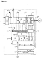
- FIG. 10 is a block diagram showing a configuration of a circuit in a conventional inverter apparatus.
- the inverter apparatus is composed of a converter 1 connected to a two- or three-phase alternate power supply to convert an alternate current into a direct current; an electrolytic capacitor 2 for smoothing; an IPM 3; a control circuit consisting of a central processing unit 6 (CPU ⁇ ROM) including a buffer 4, a controller 5, and a memory; a power supply circuit for the IPM 3 and control circuit consisting of a switching transistor 7, transistors 8, 9, and a switching regulator 10; and a current transformer CT installed between an output of the IPM 3 and a motor M.
- CPU ⁇ ROM central processing unit 6
- the IPM 3 is integrally composed of a three-phase inverter 11 that is composed of a power element and that provides an output connected to the motor M; a predriver 12 for controlling and driving the inverter 11; a protect circuit 13; a sensor 14 for detecting an overcurrent; a sensor 15 for detecting overheating; a braking power element 16 and a resistor 17 that are used to provide deceleration control for the motor M; and a predriver 18 for controlling and driving the braking power element 16.
- a control signal from the control circuit to the IPM 3 is supplied from the buffer 4 to the predrivers 12, 18 via a photocoupler, and an alarm signal issued when the sensor 14, 15 detects an overcurrent or overheated condition is supplied from the protect circuit 13 to the buffer 4 via the photocoupler.
- an output from the current transformer CT is connected to the controller 5.
- the current transformer CT detects an output current flowing from the IPM 3 to the motor M in order to return this current to the controller 5 for various forms of control.
- the current transformer CT has three through-holes therein, and is provided in the inverter apparatus in such a manner that wires or bars that act as output-current lines from the inverter 11 are inserted through these through-holes.
- a direct voltage converted by the converter 1 is converted by the inverter 11 into an alternate voltage supplied to the motor M.
- bridges are assembled using IGBTs (Insulated Gate Bipolar Transistors) and diodes, and the IGBTs chopping-control a direct current to allow an alternate current to consequently flow through the motor. By varying the frequency of this alternate current, the motor's rotation speed can be varied.
- an inverter output current detected by the current transformer CT is input to the controller 5, which then provides control such that the waveform of the output current will not be distorted or such that the output voltage will not exceed a predetermined value.
- FIG 11 is a block diagram showing a power conversion circuit in a conventional inverter apparatus.
- the power conversion circuit is composed of two modules, that is, the converter 1 and the IPM 3 including the inverter 11.
- Module terminals 21 to 25, which are shown by a circle, are provided for the converter 1 as I/O terminals, and module terminals 26 to 30 are provided for the IPM 3.
- terminal blocks R, S, T, P1, P2, N, U, V, and W which are shown by large black circles, are provided as I/O terminals for the inverter apparatus including the converter 1 and the IPM 3.
- the module terminals 21 to 30 of the converter 1 and IPM 3 are connected to the corresponding terminal blocks, and these connections are carried out by, for example, screwing copper bars to the blocks.
- the connections between the converter 1 and the inverter 11, that is, the connections between the terminal blocks P1 and P2 and between the module terminals 25 and 27 are also carried out by screwing copper bars to the blocks.
- the current transformer built into the conventional inverter apparatus to monitor an output current is relatively larger than the other components and thus requires a large installation space, thereby hindering the development of more compact inverter apparatuses.
- the wires or bars acting as output current lines must be inserted through the current transformer, the number of assembly steps is so large that the process becomes complicated.
- the apparatus since the module terminals and the terminal blocks are connected together by screwing wire rods such as copper bars, the apparatus requires a large number of set screws for connections, a complex wiring pattern, and a large number of assembly steps. In addition, an installation space must be provided for the wiring, and this constitutes a constraint on space-saving efforts.
- the present invention has been provided in view of these points. It is intended to provide a semiconductor device that can provide added space for the incorporated devices and that can reduce requirements for both wiring space and the number of assembly steps.
- the present invention provides a semiconductor device comprising a power semiconductor, a drive circuit, and a protection circuit that are integrated into the same package, characterized in that the device comprises a shunt resistor provided in series with output lines from the power semiconductor to detect an output current; and control pins that can be drawn from both ends of the shunt resistor through a wiring pattern and connected to an external device.
- the output current from the semiconductor device can be output to an external device through the control pins as the end-to-end voltage of the shunt resistor.
- This configuration enables the output current to be detected without a separate current transformer requiring a large installation space, thereby providing added space for the apparatus into which this semiconductor device is integrated.
- the present invention provides a semiconductor device comprising a power semiconductor, a drive circuit, and a protect circuit that are integrated into the same package, characterized in that at least some of the module terminals connected to a main circuit of the power semiconductor are configured as terminal blocks of an apparatus into which this semiconductor device is integrated.
- the module terminals of the semiconductor device are integrated with the terminal blocks of the apparatus into which this semiconductor device is integrated, thereby eliminating the needs for the wire rods and set screws for connections used to connect the module terminals and terminal blocks. As a result, both the wiring space and the number of assembly steps can be reduced.
- the inverter apparatus shown in Figure 1 has almost the same configuration and effects as the conventional inverter apparatus shown in Figure 10.
- components used in the conventional inverter apparatus are assigned the same reference numerals and their details are omitted.
- the differences between this inverter apparatus and the conventional inverter apparatus are twofold: first, a shunt resistor 31 is built into the IPM 3 in such a way as to be inserted in series with output lines from the IPM 3; and second, an insulating amplifier 32 or a voltage-resistant IC replacing the insulating amplifier is provided to return a terminal voltage of the shunt resistor 31 to the controller 5.
- the shunt resistor 31 has both ends wired to control pins of the IPM 3 via a pattern.
- the shunt resistor 31 can provide an output current to the controller 5 as a voltage value and monitor an output current flowing through the motor M as in a current transformer.
- the current transformer can be omitted from the inverter to reduce the installation space, the number of wiring steps, and thus the size of the apparatus.
- the shunt resistor 31 can radiate heat efficiently.
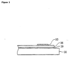
- FIG. 2 shows an example of a configuration of an IPM near a shunt resistor.
- the shunt resistor 31 is composed of an insulating layer 33, an adhesion layer 34, and a resistor 35.
- the shunt resistor 31 is mounted on an insulating substrate 36 together with functional elements constituting the IPM 3, that is, power elements of the inverter 11. Those elements such as the predrivers 12, 18 and a protection circuit that do not require radiation are mounted on a printed circuit board separate from the insulating substrate 36.
- the insulating substrate 36 may comprise a metal insulating substrate, this embodiment uses a ceramic substrate having a copper circuit pattern formed on its surface, with the shunt resistor 31 joined with the substrate via a solder 37.
- the insulating substrate 36 is joined with a copper base 38 via a solder 39.
- the shunt resistor 31 is soldered to the insulating substrate 36 of the IPM 3, and heat generated in the shunt resistor is radiated via the insulating substrate 36 and the copper base 38.
- the shunt resistor 31 built into the IPM 3 improves the latter's radiating capability to enable it to be applied when high-current output of 50 A or more is required.
- FIG 3 shows another example of a configuration of an IPM near a shunt resistor.
- the shunt resistor 31 is configured by directly depositing the resistor 35 onto the insulating substrate 36 joined with the copper base 38 via the solder 39. In this manner, by directly forming the shunt resistor 31 on the insulating substrate 36, the heat resistance between the resistor 35 and the copper base 38 decreases to improve the IPM's radiating capability.
- This configuration can restrain temperature rises in the shunt resistor 31 and improve the inverter's load tolerance.
- the resistor 35 is formed on the insulating substrate 36 by means of deposition, the resistor 35 may be joined with the insulating substrate 36 by means of pressure contact, adhesion, brazing, or an active metal method.
- the shunt resistor 31 has been mounted on the insulating substrate 36 as described above, the IPM 3 on which the shunt resistor 31 is mounted are manufactured so as to have different output currents depending on the specification of the inverter to which the IPM is applied.
- the resistance value of the shunt resistor 31 must be varied depending on the rated output current of the IPM 3. Consequently, a plurality of shunt resistors having different resistance values are provided so that a shunt resistor having an optimal resistance value is used as required. In this case, however, due to the large number of resistance values required, handling of the shunt resistor becomes quite cumbersome, as does stock management.
- the present invention uses only one shunt resistor 31, and adjusts the resistance value by varying the bonding positions of the wire. The details are described below.
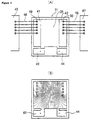
- Figure 4 is a top view of the shunt resistor.
- Figure 4(A) shows that bonding positions are evenly arranged and Figure 4(B) shows equipotential lines.
- the shunt resistor 31 is composed of the resistor 35, conductive bonding regions 41, 42 placed on the respective sides of the resistor 35, and conductive sense terminals 43, 44 connected to part of the respective sides of the resistor 35.
- the bonding region 41 is connected via a bonding wire 46 to a circuit pattern 45 on the insulating substrate 36 that corresponds to a current output line of the inverter 11.
- the bonding region 42 is connected via a bonding wire 48 to a circuit pattern 47 on the insulating substrate 36 that corresponds to a current output line leading to an output of the IPM 3.
- the sense terminals 43, 44 are connected to a circuit pattern on the insulating substrate 36 that leads to control pins of the IPM 3, which are connected to the controller 5 via an external device, in this example, the insulating amplifier 32.
- the voltage between the sense terminals 43 and 44 was 250 mV. This indicates the resistance value of the resistor 35 is 2.5 m ⁇ as seen from between the sense terminals 43 and 44.
- Figure 5 is a top view of the shunt resistor.
- Figure 5(A) shows that the bonding positions are biased to a side opposed to the sense terminals
- Figure 5(B) shows the relevant equipotential lines.
- the bonding positions 49, 50 are closely arranged in the bonding regions 41, 42 away from the sense terminals 43, 44.
- the current density and the current path are concentrated between the bonding positions 49 and 50, and the current density decreases as the distance between these positions increases.
- the equipotential lines in the resistor 35 are distributed in parallel only between the bonding positions, and the interval between the equipotential lines is larger on the side of the resistor closer to the sense terminals 43, 44, as shown in Figure 5(B).
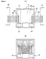
- Figure 6 is a top view of the shunt resistor.
- Figure 6(A) shows that the bonding positions are biased to the sense terminals
- Figure 6(B) shows the equipotential lines.
- the bonding positions 49, 50 of the bonding wires 46, 48 are closely arranged in the bonding regions 41, 42 near the sense terminals 43, 44, the current density and the current path concentrate between the bonding positions 49 and 50, and the equipotential lines in the resistor 35 are distributed as shown in Figure 6(B).
- one type of shunt resistor can be used to provide different resistance values, thereby eliminating the need to prepare a shunt resistor of a specific resistance value to meet the specifications of the inverter.
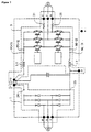
- FIG. 7 is a block diagram showing a power conversion circuit in the inverter apparatus.
- the power conversion circuit is composed of the two modules, that is, the converter 1 and the IPM 3.
- the converter 1 comprises the module terminals as its I/O terminals, and of these terminals, the input terminals and positive-pole input terminals are integrated with the alternate-input terminal blocks R, S, T, P1 of the inverter apparatus, thereby eliminating the need for the copper bars and their set screws.
- the module terminals 24, 25 of the converter 1 are connected to an electrolytic capacitor.
- the input-side module terminals are integrated with the direct-input terminal blocks P2, N of the inverter apparatus, and the output-side module terminals are integrated with the terminal blocks U, V, W.
- module terminals P(+)1, P(+)2, N(-)1, N(-)2 are provided in the immediate neighbourhood of an IGBT constituting the inverter 11 of the IPM 3.
- These module terminals P(+)1, P(+)2, N(-)1, N(-)2 are connected to a capacitor for a snubber circuit for restraining a surge voltage generated upon a switching operation of the IGBT.
- the input-side module terminals of the IPM 3 are integrated with the terminal blocks P2, N, so the wires between the terminal blocks P2, N and the IGBTs tend to be long, thereby increasing the inductances L1, L2 of the internal wires between the terminal blocks P2, N and the IGBT.
- the inductances L1, L2 of the wires may cause a large surge voltage to be generated upon a switching operation of the IGBT, thus destroying the IGBT.
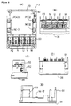
- Figure 8 shows an example of the IPM's appearance.
- Figure 8(A) is a top view
- Figure 8(B) is a front view
- Figure 8(C) is a partial sectional view of the terminal block
- Figure 8(D) is a rear view
- Figure 8(E) is a right-side view.
- the IPM 3 comprises on a frame mounted in an outer circumferential portion of the copper base 38, the inverter apparatus terminal blocks P2, N, U, V, W integrated with the module terminals of the IPM, the module terminals P(+)1, P(+)2, N(-)1, N(-)2 for the snubber circuit, and a connector 51 having control pins connected to an external control circuit.
- Two sets of the terminals blocks P2, N, U, V, W are provided, wherein one set is provided on the top surface of the frame, while the other is provided on the front surface of the frame.
- the IGBT, predrivers 12, 18, protect circuit 13, and shunt resistor 31 formed on the insulating substrate 36 are located at the centre of the frame and are sealed by a cover 52.
- the terminal block P2 is connected to the terminal block P1 and electrolytic capacitor of the converter 1, and the terminal blocks U, V, W are connected to the motor M.
- the module terminals P(+)1, P(+)2, N(-)1, N(-)2 for the snubber circuit are separately provided and connected to the circuit pattern located in the immediate neighbourhood of the IGBT. Consequently, even if the module terminals and the terminal blocks of the inverter apparatus are integrated together to increase the length of the internal wires 53 between the terminal blocks and the IGBT and thus the inductances of the internal wires 53, the snubber circuit operates in the immediate neighbourhood of the IGBT to directly restrain surge voltages generated upon switching. As a result, the presence of any inductance can be substantially neglected to reliably prevent the IGBT from being destroyed by a surge voltage.
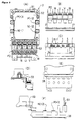
- Figure 9 shows another example of the appearance of the IPM.
- Figure 9(A) is a top view
- Figure 9(B) is a front view
- Figure 9(C) is a rear view
- Figure 9(D) is a partial sectional view of the terminal block
- Figure 9(E) is a bottom view of the neighbourhood of the terminal block
- Figure 9(E) is a right-side view.
- the IPM 3 comprises the inverter apparatus terminal blocks P2, N, U, V, W integrated with the module terminals of the IPM, the module terminals P(+)1, P(+)2, N(-)1, N(-)2 for the snubber circuit, and the connector 51 having control pins for connection to an external control circuit.
- Two sets of the terminals blocks P2, N, U, V, W are provided on the top side of the frame.
- the IGBT, predrivers 12, 18, protect circuit 13, and shunt resistor 31 formed on the insulating substrate 36 are located at the centre of the frame and are sealed by the cover 52.
- the module terminals P(+)1, N(-)1 and P(+)2, N(-)2 are directly connected to the two capacitors for the snubber circuit placed on the cover 52.
- the terminal block P2 is connected to the terminal block P1 and electrolytic capacitor of the converter 1, and the terminal blocks U, V, W are connected to the motor M.
- the module terminals and the terminal blocks of the inverter apparatus are also integrated together via the internal wires 53 to eliminate the needs for copper bars and their mounting screws for wiring.
- the module terminals P(+)1, P(+)2, N(-)1, N(-)2 for the snubber circuit are connected to the circuit pattern located in the immediate neighbourhood of the IGBT, the snubber circuit operates in the immediate neighbourhood of the IGBT to enable the effects of any inductance for wires between the terminal blocks of the inverter apparatus and the IGBT to be neglected.
- the present invention is configured to incorporate a shunt resistor for detecting an output current, both ends of which can be connected to an external device.
- This configuration enables the inverter apparatus to omit the current transformer and thus to reduce requirements for both installation space and the number of wiring steps, and also to enable the output current to be controlled based on the detected voltage, using a connection with the external device.
- the apparatus's radiating capability can be improved by providing the shunt resistor on the insulating substrate with the power elements mounted thereon, so the present invention can be applied to an inverter apparatus designed for high currents of 50 A and.
- the present invention can eliminate the effects of any wire inductance associated with the longer wire lengths required for integration of the module terminals and the terminal blocks.
Landscapes
- Inverter Devices (AREA)
- Semiconductor Integrated Circuits (AREA)
- Power Conversion In General (AREA)
- Lead Frames For Integrated Circuits (AREA)
- Amplifiers (AREA)
Priority Applications (2)
| Application Number | Priority Date | Filing Date | Title |
|---|---|---|---|
| EP08167298A EP2015361B1 (de) | 1998-12-09 | 1999-11-24 | Halbleitervorrichtung |
| EP08167294A EP2012357B1 (de) | 1998-12-09 | 1999-11-24 | Verfahren zur Herstellung einer Halbleitervorrichtung |
Applications Claiming Priority (2)
| Application Number | Priority Date | Filing Date | Title |
|---|---|---|---|
| JP34959798A JP3548024B2 (ja) | 1998-12-09 | 1998-12-09 | 半導体装置およびその製造方法 |
| JP34959798 | 1998-12-09 |
Related Child Applications (4)
| Application Number | Title | Priority Date | Filing Date |
|---|---|---|---|
| EP08167298A Division EP2015361B1 (de) | 1998-12-09 | 1999-11-24 | Halbleitervorrichtung |
| EP08167294A Division EP2012357B1 (de) | 1998-12-09 | 1999-11-24 | Verfahren zur Herstellung einer Halbleitervorrichtung |
| EP08167294.1 Division-Into | 2008-10-22 | ||
| EP08167298.2 Division-Into | 2008-10-22 |
Publications (3)
| Publication Number | Publication Date |
|---|---|
| EP1009030A2 true EP1009030A2 (de) | 2000-06-14 |
| EP1009030A3 EP1009030A3 (de) | 2001-10-17 |
| EP1009030B1 EP1009030B1 (de) | 2010-09-29 |
Family
ID=18404813
Family Applications (3)
| Application Number | Title | Priority Date | Filing Date |
|---|---|---|---|
| EP08167298A Expired - Lifetime EP2015361B1 (de) | 1998-12-09 | 1999-11-24 | Halbleitervorrichtung |
| EP99309398A Expired - Lifetime EP1009030B1 (de) | 1998-12-09 | 1999-11-24 | Halbleiteranordnung mit einem Leistungselement und einer Schutzschaltung |
| EP08167294A Expired - Lifetime EP2012357B1 (de) | 1998-12-09 | 1999-11-24 | Verfahren zur Herstellung einer Halbleitervorrichtung |
Family Applications Before (1)
| Application Number | Title | Priority Date | Filing Date |
|---|---|---|---|
| EP08167298A Expired - Lifetime EP2015361B1 (de) | 1998-12-09 | 1999-11-24 | Halbleitervorrichtung |
Family Applications After (1)
| Application Number | Title | Priority Date | Filing Date |
|---|---|---|---|
| EP08167294A Expired - Lifetime EP2012357B1 (de) | 1998-12-09 | 1999-11-24 | Verfahren zur Herstellung einer Halbleitervorrichtung |
Country Status (4)
| Country | Link |
|---|---|
| US (1) | US6262902B1 (de) |
| EP (3) | EP2015361B1 (de) |
| JP (1) | JP3548024B2 (de) |
| DE (3) | DE69942796D1 (de) |
Cited By (4)
| Publication number | Priority date | Publication date | Assignee | Title |
|---|---|---|---|---|
| DE10143932A1 (de) * | 2001-09-07 | 2003-04-03 | Eupec Gmbh & Co Kg | Shunt-Widerstandanordnung |
| EP1909377A4 (de) * | 2006-01-16 | 2009-06-17 | Mitsubishi Electric Corp | Motoransteuerung und ausseneinheit einer klimaanlage |
| CN102263512A (zh) * | 2010-05-25 | 2011-11-30 | 李尔公司 | 带有电流感测的电源模块 |
| CN102999009A (zh) * | 2012-12-11 | 2013-03-27 | 深圳市麦格米特驱动技术有限公司 | 机床控制电路 |
Families Citing this family (25)
| Publication number | Priority date | Publication date | Assignee | Title |
|---|---|---|---|---|
| JP3826749B2 (ja) * | 2001-08-22 | 2006-09-27 | 株式会社日立製作所 | シャント抵抗を備えた電力変換装置 |
| AU2002341359A1 (en) * | 2001-09-27 | 2003-04-07 | Galil Medical Ltd. | Apparatus and method for cryosurgical treatment of tumors of the breast |
| JP2003218318A (ja) * | 2002-01-21 | 2003-07-31 | Mitsubishi Electric Corp | 半導体パワーモジュール、半導体パワーモジュールに用いる絶縁基板及び該絶縁基板の製造方法 |
| US6653812B1 (en) | 2002-01-31 | 2003-11-25 | Analog Devices, Inc. | Space vector modulation methods and structures for electric-motor control |
| JP4236909B2 (ja) * | 2002-11-13 | 2009-03-11 | 三菱電機株式会社 | 電力半導体モジュール |
| US20040227476A1 (en) * | 2002-12-19 | 2004-11-18 | International Rectifier Corp. | Flexible inverter power module for motor drives |
| JP2004343820A (ja) * | 2003-05-13 | 2004-12-02 | Mitsubishi Electric Corp | 電力変換装置 |
| KR100669327B1 (ko) * | 2004-10-11 | 2007-01-15 | 삼성에스디아이 주식회사 | 플라즈마 디스플레이 장치 |
| US7619302B2 (en) * | 2006-05-23 | 2009-11-17 | International Rectifier Corporation | Highly efficient both-side-cooled discrete power package, especially basic element for innovative power modules |
| JP5354144B2 (ja) * | 2007-10-22 | 2013-11-27 | 東芝キヤリア株式会社 | インバータ |
| JP5800192B2 (ja) * | 2011-10-11 | 2015-10-28 | 富士電機株式会社 | フォトカプラの出力信号受信回路 |
| DE102012211924B4 (de) * | 2012-07-09 | 2014-02-13 | Infineon Technologies Ag | Halbleitermodul mit einem in einer Anschlusslasche integrierten Shunt-Widerstand und Verfahren zur Ermittlung eines durch einen Lastanschluss eines Halbleitermoduls fließenden Stromes |
| JP5930954B2 (ja) * | 2012-12-14 | 2016-06-08 | 三菱電機株式会社 | パワーモジュール |
| US9140735B2 (en) | 2013-05-03 | 2015-09-22 | Infineon Technologies Ag | Integration of current measurement in wiring structure of an electronic circuit |
| JPWO2015005181A1 (ja) * | 2013-07-08 | 2017-03-02 | 株式会社村田製作所 | 電力変換部品 |
| JP2015073261A (ja) * | 2013-09-03 | 2015-04-16 | ルネサスエレクトロニクス株式会社 | 半導体装置 |
| JP6487280B2 (ja) | 2015-06-11 | 2019-03-20 | ルネサスエレクトロニクス株式会社 | 半導体装置 |
| JP6894181B2 (ja) * | 2015-06-17 | 2021-06-30 | ダイキン工業株式会社 | インバータ装置 |
| CN105609493B (zh) * | 2016-03-22 | 2018-05-11 | 富士电机(中国)有限公司 | 一种集成双向升降压功能的八合一igbt模块 |
| JP6691416B2 (ja) * | 2016-04-04 | 2020-04-28 | ダイキン工業株式会社 | 電子回路装置 |
| CN110800104A (zh) * | 2017-06-22 | 2020-02-14 | 三菱电机株式会社 | 半导体模块 |
| CN109861501A (zh) * | 2019-03-25 | 2019-06-07 | 广东美的制冷设备有限公司 | 智能功率模块和空调器 |
| WO2020191848A1 (zh) * | 2019-03-25 | 2020-10-01 | 广东美的制冷设备有限公司 | 集成式控制器及其控制方法和制冷设备 |
| JP2022179872A (ja) * | 2021-05-24 | 2022-12-06 | 富士電機株式会社 | 半導体装置 |
| JP7426676B2 (ja) | 2022-02-08 | 2024-02-02 | パナソニックIpマネジメント株式会社 | 半導体パッケージ |
Family Cites Families (10)
| Publication number | Priority date | Publication date | Assignee | Title |
|---|---|---|---|---|
| US3676807A (en) * | 1971-05-19 | 1972-07-11 | Tektronix Inc | Film attenuator with distributed capacitance high frequency compensation |
| JPH0231457A (ja) * | 1988-07-21 | 1990-02-01 | Matsushita Electric Ind Co Ltd | 発光素子駆動用半導体装置 |
| JPH0834705B2 (ja) * | 1988-11-16 | 1996-03-29 | 株式会社大林組 | 開閉器 |
| JP2658427B2 (ja) * | 1989-01-17 | 1997-09-30 | 富士電機株式会社 | 電力変換用半導体素子のスナバ回路とそのモジュール装置 |
| US5214407A (en) * | 1991-11-06 | 1993-05-25 | Hewlett-Packard Company | High performance current shunt |
| JP2979930B2 (ja) * | 1993-10-28 | 1999-11-22 | 富士電機株式会社 | 電力用半導体装置のパッケージ |
| JP3325697B2 (ja) | 1994-01-20 | 2002-09-17 | 三菱電機株式会社 | パワーデバイスの制御装置およびモータの駆動制御装置 |
| JPH09312376A (ja) * | 1996-05-21 | 1997-12-02 | Fuji Electric Co Ltd | 半導体装置 |
| EP1028520A4 (de) * | 1996-09-06 | 2000-08-16 | Hitachi Ltd | Halbleiteranordnung |
| JP3008924B2 (ja) * | 1998-04-10 | 2000-02-14 | 富士電機株式会社 | パワー素子のドライブ回路 |
-
1998
- 1998-12-09 JP JP34959798A patent/JP3548024B2/ja not_active Expired - Lifetime
-
1999
- 1999-11-23 US US09/447,806 patent/US6262902B1/en not_active Expired - Lifetime
- 1999-11-24 EP EP08167298A patent/EP2015361B1/de not_active Expired - Lifetime
- 1999-11-24 DE DE69942796T patent/DE69942796D1/de not_active Expired - Lifetime
- 1999-11-24 EP EP99309398A patent/EP1009030B1/de not_active Expired - Lifetime
- 1999-11-24 DE DE69942812T patent/DE69942812D1/de not_active Expired - Lifetime
- 1999-11-24 DE DE69942813T patent/DE69942813D1/de not_active Expired - Lifetime
- 1999-11-24 EP EP08167294A patent/EP2012357B1/de not_active Expired - Lifetime
Cited By (7)
| Publication number | Priority date | Publication date | Assignee | Title |
|---|---|---|---|---|
| DE10143932A1 (de) * | 2001-09-07 | 2003-04-03 | Eupec Gmbh & Co Kg | Shunt-Widerstandanordnung |
| US6756877B2 (en) | 2001-09-07 | 2004-06-29 | Infineon Technologies Ag | Shunt resistor configuration |
| DE10143932B4 (de) * | 2001-09-07 | 2006-04-27 | eupec Europäische Gesellschaft für Leistungshalbleiter mbH & Co. KG | Shunt-Widerstandanordnung |
| EP1909377A4 (de) * | 2006-01-16 | 2009-06-17 | Mitsubishi Electric Corp | Motoransteuerung und ausseneinheit einer klimaanlage |
| US7643296B2 (en) | 2006-01-16 | 2010-01-05 | Mitsubishi Electric Corporation | Motor drive circuit and outdoor unit for air conditioner |
| CN102263512A (zh) * | 2010-05-25 | 2011-11-30 | 李尔公司 | 带有电流感测的电源模块 |
| CN102999009A (zh) * | 2012-12-11 | 2013-03-27 | 深圳市麦格米特驱动技术有限公司 | 机床控制电路 |
Also Published As
| Publication number | Publication date |
|---|---|
| DE69942812D1 (de) | 2010-11-11 |
| EP1009030B1 (de) | 2010-09-29 |
| DE69942796D1 (de) | 2010-11-11 |
| DE69942813D1 (de) | 2010-11-11 |
| US6262902B1 (en) | 2001-07-17 |
| EP2012357A3 (de) | 2009-07-29 |
| JP3548024B2 (ja) | 2004-07-28 |
| JP2000174202A (ja) | 2000-06-23 |
| EP2012357B1 (de) | 2010-09-29 |
| EP2012357A2 (de) | 2009-01-07 |
| EP2015361B1 (de) | 2010-09-29 |
| EP2015361A2 (de) | 2009-01-14 |
| EP1009030A3 (de) | 2001-10-17 |
| EP2015361A3 (de) | 2009-07-29 |
Similar Documents
| Publication | Publication Date | Title |
|---|---|---|
| EP1009030B1 (de) | Halbleiteranordnung mit einem Leistungselement und einer Schutzschaltung | |
| CN110199388B (zh) | 用于并联功率装置的具有低电感和快速切换的高功率多层模块 | |
| US6313598B1 (en) | Power semiconductor module and motor drive system | |
| EP1160866B1 (de) | Halbleiterelement mit Leistungsverdrahtungsstruktur | |
| US7542318B2 (en) | Capacitor mounting type inverter unit having a recessed cover | |
| US6373705B1 (en) | Electronic semiconductor module | |
| EP0697732B1 (de) | Steuerschaltungsmodul | |
| CN112968025B (zh) | 智能功率模块和智能功率模块的制造方法 | |
| JP2024543417A (ja) | 小型パワーモジュール | |
| US20050197799A1 (en) | Temperature detection method of semiconductor device and power conversion apparatus | |
| US10438874B2 (en) | Power conversion device | |
| EP0987762B1 (de) | Halbleitermodul | |
| JP3941266B2 (ja) | 半導体パワーモジュール | |
| US6795324B2 (en) | Power converter | |
| US5896286A (en) | Power semiconductor module | |
| JPH1118429A (ja) | 制御モジュール | |
| JP4631179B2 (ja) | 半導体装置およびこれを用いたインバータ装置 | |
| CN112968622A (zh) | 智能功率模块及采用其的智能功率模块结构 | |
| EP0527033B1 (de) | Halbleitermodul | |
| JP3747931B2 (ja) | 半導体装置 | |
| CN214480328U (zh) | 智能功率模块及采用其的智能功率模块结构 | |
| JP4246040B2 (ja) | 半導体装置の実装体 | |
| US12489095B2 (en) | Semiconductor apparatus | |
| JPH09135155A (ja) | 半導体装置 | |
| WO2022097533A1 (ja) | 放電回路モジュール |
Legal Events
| Date | Code | Title | Description |
|---|---|---|---|
| PUAI | Public reference made under article 153(3) epc to a published international application that has entered the european phase |
Free format text: ORIGINAL CODE: 0009012 |
|
| AK | Designated contracting states |
Kind code of ref document: A2 Designated state(s): AT BE CH CY DE DK ES FI FR GB GR IE IT LI LU MC NL PT SE Kind code of ref document: A2 Designated state(s): DE FR GB |
|
| AX | Request for extension of the european patent |
Free format text: AL;LT;LV;MK;RO;SI |
|
| PUAL | Search report despatched |
Free format text: ORIGINAL CODE: 0009013 |
|
| AK | Designated contracting states |
Kind code of ref document: A3 Designated state(s): AT BE CH CY DE DK ES FI FR GB GR IE IT LI LU MC NL PT SE |
|
| AX | Request for extension of the european patent |
Free format text: AL;LT;LV;MK;RO;SI |
|
| 17P | Request for examination filed |
Effective date: 20011229 |
|
| AKX | Designation fees paid |
Free format text: DE FR GB |
|
| 17Q | First examination report despatched |
Effective date: 20071126 |
|
| RAP1 | Party data changed (applicant data changed or rights of an application transferred) |
Owner name: FUJI ELECTRIC SYSTEMS CO., LTD. |
|
| GRAP | Despatch of communication of intention to grant a patent |
Free format text: ORIGINAL CODE: EPIDOSNIGR1 |
|
| GRAS | Grant fee paid |
Free format text: ORIGINAL CODE: EPIDOSNIGR3 |
|
| GRAA | (expected) grant |
Free format text: ORIGINAL CODE: 0009210 |
|
| AK | Designated contracting states |
Kind code of ref document: B1 Designated state(s): DE FR GB |
|
| REG | Reference to a national code |
Ref country code: GB Ref legal event code: FG4D |
|
| REF | Corresponds to: |
Ref document number: 69942796 Country of ref document: DE Date of ref document: 20101111 Kind code of ref document: P |
|
| PLBE | No opposition filed within time limit |
Free format text: ORIGINAL CODE: 0009261 |
|
| STAA | Information on the status of an ep patent application or granted ep patent |
Free format text: STATUS: NO OPPOSITION FILED WITHIN TIME LIMIT |
|
| 26N | No opposition filed |
Effective date: 20110630 |
|
| REG | Reference to a national code |
Ref country code: GB Ref legal event code: 732E Free format text: REGISTERED BETWEEN 20110908 AND 20110914 |
|
| REG | Reference to a national code |
Ref country code: DE Ref legal event code: R082 Ref document number: 69942796 Country of ref document: DE Representative=s name: CHARRIER RAPP & LIEBAU PATENTANWAELTE PARTG MB, DE Effective date: 20110826 Ref country code: DE Ref legal event code: R082 Ref document number: 69942796 Country of ref document: DE Representative=s name: PATENTANWAELTE CHARRIER RAPP & LIEBAU, DE Effective date: 20110826 Ref country code: DE Ref legal event code: R081 Ref document number: 69942796 Country of ref document: DE Owner name: FUJI ELECTRIC CO., LTD., KAWASAKI-SHI, JP Free format text: FORMER OWNER: FUJI ELECTRIC SYSTEMS CO., LTD., TOKYO/TOKIO, JP Effective date: 20110826 |
|
| REG | Reference to a national code |
Ref country code: DE Ref legal event code: R097 Ref document number: 69942796 Country of ref document: DE Effective date: 20110630 |
|
| REG | Reference to a national code |
Ref country code: FR Ref legal event code: TP Owner name: FUJI ELECTRIC CO., LTD., JP Effective date: 20111021 |
|
| REG | Reference to a national code |
Ref country code: GB Ref legal event code: 746 Effective date: 20121221 |
|
| REG | Reference to a national code |
Ref country code: DE Ref legal event code: R084 Ref document number: 69942796 Country of ref document: DE Effective date: 20121219 |
|
| PGFP | Annual fee paid to national office [announced via postgrant information from national office to epo] |
Ref country code: GB Payment date: 20141119 Year of fee payment: 16 |
|
| REG | Reference to a national code |
Ref country code: FR Ref legal event code: PLFP Year of fee payment: 17 |
|
| PGFP | Annual fee paid to national office [announced via postgrant information from national office to epo] |
Ref country code: FR Payment date: 20151008 Year of fee payment: 17 |
|
| GBPC | Gb: european patent ceased through non-payment of renewal fee |
Effective date: 20151124 |
|
| PG25 | Lapsed in a contracting state [announced via postgrant information from national office to epo] |
Ref country code: GB Free format text: LAPSE BECAUSE OF NON-PAYMENT OF DUE FEES Effective date: 20151124 |
|
| REG | Reference to a national code |
Ref country code: FR Ref legal event code: ST Effective date: 20170731 |
|
| PG25 | Lapsed in a contracting state [announced via postgrant information from national office to epo] |
Ref country code: FR Free format text: LAPSE BECAUSE OF NON-PAYMENT OF DUE FEES Effective date: 20161130 |
|
| PGFP | Annual fee paid to national office [announced via postgrant information from national office to epo] |
Ref country code: DE Payment date: 20171121 Year of fee payment: 19 |
|
| REG | Reference to a national code |
Ref country code: DE Ref legal event code: R119 Ref document number: 69942796 Country of ref document: DE |
|
| PG25 | Lapsed in a contracting state [announced via postgrant information from national office to epo] |
Ref country code: DE Free format text: LAPSE BECAUSE OF NON-PAYMENT OF DUE FEES Effective date: 20190601 |