EP1010543A1 - Carte a puce et module a puce - Google Patents
Carte a puce et module a puce Download PDFInfo
- Publication number
- EP1010543A1 EP1010543A1 EP97949219A EP97949219A EP1010543A1 EP 1010543 A1 EP1010543 A1 EP 1010543A1 EP 97949219 A EP97949219 A EP 97949219A EP 97949219 A EP97949219 A EP 97949219A EP 1010543 A1 EP1010543 A1 EP 1010543A1
- Authority
- EP
- European Patent Office
- Prior art keywords
- circuit chip
- antenna
- card
- circuit
- processing unit
- Prior art date
- Legal status (The legal status is an assumption and is not a legal conclusion. Google has not performed a legal analysis and makes no representation as to the accuracy of the status listed.)
- Pending
Links
Images


Classifications
-
- B—PERFORMING OPERATIONS; TRANSPORTING
- B42—BOOKBINDING; ALBUMS; FILES; SPECIAL PRINTED MATTER
- B42D—BOOKS; BOOK COVERS; LOOSE LEAVES; PRINTED MATTER CHARACTERISED BY IDENTIFICATION OR SECURITY FEATURES; PRINTED MATTER OF SPECIAL FORMAT OR STYLE NOT OTHERWISE PROVIDED FOR; DEVICES FOR USE THEREWITH AND NOT OTHERWISE PROVIDED FOR; MOVABLE-STRIP WRITING OR READING APPARATUS
- B42D25/00—Information-bearing cards or sheet-like structures characterised by identification or security features; Manufacture thereof
- B42D25/30—Identification or security features, e.g. for preventing forgery
- B42D25/305—Associated digital information
-
- G—PHYSICS
- G06—COMPUTING OR CALCULATING; COUNTING
- G06K—GRAPHICAL DATA READING; PRESENTATION OF DATA; RECORD CARRIERS; HANDLING RECORD CARRIERS
- G06K19/00—Record carriers for use with machines and with at least a part designed to carry digital markings
- G06K19/06—Record carriers for use with machines and with at least a part designed to carry digital markings characterised by the kind of the digital marking, e.g. shape, nature, code
- G06K19/067—Record carriers with conductive marks, printed circuits or semiconductor circuit elements, e.g. credit or identity cards also with resonating or responding marks without active components
- G06K19/07—Record carriers with conductive marks, printed circuits or semiconductor circuit elements, e.g. credit or identity cards also with resonating or responding marks without active components with integrated circuit chips
- G06K19/077—Constructional details, e.g. mounting of circuits in the carrier
- G06K19/07749—Constructional details, e.g. mounting of circuits in the carrier the record carrier being capable of non-contact communication, e.g. constructional details of the antenna of a non-contact smart card
- G06K19/0775—Constructional details, e.g. mounting of circuits in the carrier the record carrier being capable of non-contact communication, e.g. constructional details of the antenna of a non-contact smart card arrangements for connecting the integrated circuit to the antenna
-
- G—PHYSICS
- G06—COMPUTING OR CALCULATING; COUNTING
- G06K—GRAPHICAL DATA READING; PRESENTATION OF DATA; RECORD CARRIERS; HANDLING RECORD CARRIERS
- G06K19/00—Record carriers for use with machines and with at least a part designed to carry digital markings
- G06K19/06—Record carriers for use with machines and with at least a part designed to carry digital markings characterised by the kind of the digital marking, e.g. shape, nature, code
- G06K19/067—Record carriers with conductive marks, printed circuits or semiconductor circuit elements, e.g. credit or identity cards also with resonating or responding marks without active components
- G06K19/07—Record carriers with conductive marks, printed circuits or semiconductor circuit elements, e.g. credit or identity cards also with resonating or responding marks without active components with integrated circuit chips
- G06K19/077—Constructional details, e.g. mounting of circuits in the carrier
- G06K19/07749—Constructional details, e.g. mounting of circuits in the carrier the record carrier being capable of non-contact communication, e.g. constructional details of the antenna of a non-contact smart card
- G06K19/07773—Antenna details
- G06K19/07775—Antenna details the antenna being on-chip
-
- G—PHYSICS
- G06—COMPUTING OR CALCULATING; COUNTING
- G06K—GRAPHICAL DATA READING; PRESENTATION OF DATA; RECORD CARRIERS; HANDLING RECORD CARRIERS
- G06K19/00—Record carriers for use with machines and with at least a part designed to carry digital markings
- G06K19/06—Record carriers for use with machines and with at least a part designed to carry digital markings characterised by the kind of the digital marking, e.g. shape, nature, code
- G06K19/067—Record carriers with conductive marks, printed circuits or semiconductor circuit elements, e.g. credit or identity cards also with resonating or responding marks without active components
- G06K19/07—Record carriers with conductive marks, printed circuits or semiconductor circuit elements, e.g. credit or identity cards also with resonating or responding marks without active components with integrated circuit chips
- G06K19/077—Constructional details, e.g. mounting of circuits in the carrier
- G06K19/07749—Constructional details, e.g. mounting of circuits in the carrier the record carrier being capable of non-contact communication, e.g. constructional details of the antenna of a non-contact smart card
- G06K19/07773—Antenna details
- G06K19/07777—Antenna details the antenna being of the inductive type
- G06K19/07779—Antenna details the antenna being of the inductive type the inductive antenna being a coil
- G06K19/07781—Antenna details the antenna being of the inductive type the inductive antenna being a coil the coil being fabricated in a winding process
-
- G—PHYSICS
- G06—COMPUTING OR CALCULATING; COUNTING
- G06K—GRAPHICAL DATA READING; PRESENTATION OF DATA; RECORD CARRIERS; HANDLING RECORD CARRIERS
- G06K19/00—Record carriers for use with machines and with at least a part designed to carry digital markings
- G06K19/06—Record carriers for use with machines and with at least a part designed to carry digital markings characterised by the kind of the digital marking, e.g. shape, nature, code
- G06K19/067—Record carriers with conductive marks, printed circuits or semiconductor circuit elements, e.g. credit or identity cards also with resonating or responding marks without active components
- G06K19/07—Record carriers with conductive marks, printed circuits or semiconductor circuit elements, e.g. credit or identity cards also with resonating or responding marks without active components with integrated circuit chips
- G06K19/077—Constructional details, e.g. mounting of circuits in the carrier
- G06K19/07749—Constructional details, e.g. mounting of circuits in the carrier the record carrier being capable of non-contact communication, e.g. constructional details of the antenna of a non-contact smart card
- G06K19/07773—Antenna details
- G06K19/07777—Antenna details the antenna being of the inductive type
- G06K19/07779—Antenna details the antenna being of the inductive type the inductive antenna being a coil
- G06K19/07783—Antenna details the antenna being of the inductive type the inductive antenna being a coil the coil being planar
-
- H—ELECTRICITY
- H10—SEMICONDUCTOR DEVICES; ELECTRIC SOLID-STATE DEVICES NOT OTHERWISE PROVIDED FOR
- H10W—GENERIC PACKAGES, INTERCONNECTIONS, CONNECTORS OR OTHER CONSTRUCTIONAL DETAILS OF DEVICES COVERED BY CLASS H10
- H10W90/00—Package configurations
- H10W90/701—Package configurations characterised by the relative positions of pads or connectors relative to package parts
- H10W90/751—Package configurations characterised by the relative positions of pads or connectors relative to package parts of bond wires
- H10W90/754—Package configurations characterised by the relative positions of pads or connectors relative to package parts of bond wires between a chip and a stacked insulating package substrate, interposer or RDL
Definitions
- the present invention relates to circuit chip mounted cards and circuit chip modules and in particular to circuit chip mounted cards and circuit chip modules using an antenna-integrated circuit chip to enhance reliability and reduce the cost for manufacturing the same.
- Non-contact IC cards are used at automatic ticket gates for ski-lifts, railroads and the like, for automatic load sorting, and the like.
- Fig. 13 shows one example of conventional, non-contact IC cards.
- An IC card 2 shown in Fig. 13 is a single-coil IC card comprised of a coil 4 used as an antenna, capacitors C1, C2, and an IC chip 8.
- Capacitors C1, C2 and IC chip 8 are mounted to a substrate of synthetic resin in the form of a film.
- the substrate with capacitors C1, C2 and IC chip 8 mounted thereto is referred to as a tape automated bonding (TAB) 10.
- TAB tape automated bonding
- Fig. 14A is a cross section of IC card 2.
- a core member 12 of synthetic resin is sandwiched between paired surface members 14 and 16.
- TAB 10 with capacitors C1, C2 and IC chip 8 mounted thereto is fixed to surface member 14 exposed in a hollow portion 18 provided in core member 12.
- a portion binding TAB 10 and IC chip 8 together is covered with a sealing member 9 of epoxy resin or the like.
- Coil 4 is arranged between surface member 14 and core member 12. Coil 4 and TAB 10 are connected together by a wire 20.
- Fig. 14B is a circuit diagram of IC card 2.
- IC card 2 an electromagnetic wave sent from a reader/writer (not shown) is received at a resonance circuit 22 comprised of coil 4 and capacitor C1 and is used as a power source.
- capacitor C2 is a power smoothing capacitor.
- a control unit (not shown) provided in IC chip 8 interprets information superposed on the electromagnetic wave to provide a response to the information.
- the response is provided by varying an impedance of resonance circuit 22.
- the reader/writer appreciates the response by detecting an impedance variation (or impedance reflection) of the reader/writer's resonance circuit (not shown) that is associated with the impedance variation of resonance circuit 22 of IC card 2.
- IC card 2 is dispensed with a power supply therein and can also provide non-contact communication of information.
- IC card 2 is often put into a purse, a pocket of pants and the like so that it can receive considerably strong bending, twisting and pressing forces.
- IC card 2 shown in Fig. 14A is, however, not sufficiently thick, having a thickness t of a standard dimension.
- IC card 2 does not have so large rigidity against bending, twisting and pressing forces. Accordingly IC card 2 is flexed significantly when it receives intense bending force or the like.
- wire 20 can be cut off or wire 20 can be disconnected from coil 4 or TAB 10. Wire 20 and coil 4 or TAB 10 can also be mutually connected unsatisfactorily in the operation to connect them together.
- TAB 10 the position of TAB 10 is limited in order to ensure the space for coil 4.
- arranging TAB 10 at a position which suffers significant flexure can sometimes not be avoided.
- IC chip 8 will also be deformed significantly. Such deformation cracks IC chip 8 and thus degrades the function of the IC card.
- a first object of the present invention is therefore to provide a circuit chip mounted card which is reliable and reduces the cost for manufacturing the same.
- a second object of the present invention is to provide a circuit chip module which is reliable and reduces the cost for manufacturing the same.
- a circuit chip mounted card in one aspect of the present invention includes an antenna using an electromagnetic wave to allow communication and a processing unit providing a process associated with the communication, characterized in that the antenna is provided internal or external to the processing unit containing the circuit chip such that the antenna is substantially integrated with the circuit chip.
- communicating function can be completely provided merely by a single circuit chip with the function of the processing unit and that of the antenna substantially integrated therewith.
- the circuit chip does not require external wiring and is thus free of unsatisfactory connection associated with an operation to connect external wires. Furthermore, such accidents as cutting-off, disconnection and the like of external wires cannot happen if the card is flexed.
- the substantial integration of the antenna with the circuit chip can prevents the position of the circuit chip from being limited to ensure the space for the antenna.
- the small-area circuit chip with the antenna integrated can be arranged at any position free of significant flexure. As a result, the circuit chip is not deformed significantly if the card receives significant force.
- circuit chip mounted card can be provided which is highly reliable and reduces the cost for manufacturing the same.
- the circuit chip has on its surface a terminal electrically connected to the processing unit incorporated therein and the antenna formed by fixing a metal wire on a film is arranged in contact with the surface of the circuit chip and is also electrically connected to the terminal at the surface of the chip.
- relatively simple techniques such as printing, etching
- relatively simple bonding techniques such as bumping, soldering
- bumping, soldering can also be used to connect the terminal and the antenna together.
- the antenna and the circuit chip can relatively readily be integrated together.
- the circuit chip has on its surface a terminal electrically connected to the processing unit incorporated therein and the antenna provided by winding a metal wire around the circuit chip is electrically connected to the terminal at the surface of the chip.
- the circuit chip has on its surface a terminal electrically connected to the processing unit incorporated therein and the antenna provided by fixing a metal wire on a surface of the circuit chip is electrically connected to the terminal at the surface of the chip.
- relatively simple techniques such as printing, etching, can be used to provide the antenna directly on a surface of the circuit chip.
- a pattern for printing the antenna can be formed to also connect the antenna and the terminal together when the antenna is being constructed. This eliminates the necessity of providing a separate step of connecting the antenna and the terminal together and thus further facilitates the integration of the antenna with the circuit chip. Furthermore the reduced number of the manufacturing process steps can also reduce defects and enhance the reliability of the circuit chip mounted card.
- the antenna is constructed of a wiring layer provided in the circuit chip and the antenna is electrically connected in the circuit chip to the processing unit.
- a wiring layer constructing technique is employed in the circuit chip to construct the antenna in the circuit chip. Since communicating function is completely provided in the circuit chip, it is not necessary to provide an operation or the like to construct the antenna after the construction of the circuit chip. Thus the cost for manufacturing the card can further be reduced.
- the antenna that is not exposed external to the circuit chip can be prevented from being accidentally cut off when it is mounted to the card.
- the reliability of the circuit chip mounted card is further enhanced.
- the resonance circuit provided in the circuit chip and comprised of a capacitor and a coil corresponding to an antenna has an adjustable resonance frequency.
- the capacitance or inductance of the resonance circuit can be adjusted after the capacitor and the coil are provided in the circuit chip. This allows resonance frequency to be adjusted after the circuit elements configuring the resonance circuit are all constructed in the circuit chip.
- the resonance frequency can be constant to some extent and the reliability of the circuit chip mounted card can further be enhanced. Furthermore a circuit chip accommodating a wide range of resonance frequencies can be obtained without changing a masking pattern for forming a circuit element thereof in the process of manufacturing the same, so that the cost for manufacturing the same can be reduced.
- the circuit chip has a plurality of capacitors previously constructed therein and having an interconnect selectively connected to obtain a desired resonance frequency.
- resonance frequency can readily be adjusted as desired.
- the circuit chip has a plurality of coils previously constructed therein and having an interconnect selectively connected to obtain a desired resonance frequency.
- resonance frequency can readily be adjusted as desired.
- a circuit chip mounted card in a second aspect of the present invention is a circuit chip mounted card mounting thereto an antenna using an electromagnetic wave to provide communication and a processing unit providing a process associated with the communication, comprised of a first base member, a second base member, a core member layer, a circuit chip and an antenna.
- the second base member is spaced apart from the first base member by a predetermined distance in the direction of the thickness of the card.
- the core member layer is arranged between the first base member and the second base member.
- the circuit chip is provided with the processing unit therein, and a terminal provided on a surface thereof and electrically connected to the processing unit.
- the antenna formed by fixing a metal wire on a film, is arranged on a surface of the circuit chip and electrically connected to the terminal on the surface of the circuit chip.
- the circuit chip and the antenna are arranged at the core member layer.
- circuit chip With the configuration, communication can be provided simply via a circuit chip with the function of the processing unit and that of the antenna substantially integrated therewith.
- the circuit chip does not require external wiring and can thus be free of unsatisfactory connection, cutting-off and the like of external wires.
- the elimination of the connection of external wires can also facilitate the fabrication of the card.
- circuit chip Furthermore it is not necessary to limit the position of the circuit chip to ensure the space for the antenna.
- circuit chip can be arranged at a location free of significant flexure so as to prevent deformation of the circuit chip.
- circuit chip mounted card can be provided which is highly reliable and reduces the cost for manufacturing the same.
- a circuit chip mounted card in a third aspect of the present invention is a card mounting thereto an antenna using an electromagnetic wave to provide communication and a processing unit providing a process associated with the communication, comprised of a first base member, a second base member, a core member layer, a circuit chip and an antenna.
- the second base member is spaced apart from the first base member by a predetermined distance in the direction of the thickness of the card.
- the core member layer is arranged between the first base member and the second base member.
- the circuit chip is provided with the processing unit therein and a terminal provided on a surface thereof and electrically connected to the processing unit.
- the antenna is constructed by winding a metal wire around the circuit chip and is also electrically connected to the terminal on the surface of the circuit chip.
- the circuit chip and the antenna are arranged at the core member layer.
- circuit chip With the configuration, communication can be provided simply via a circuit chip with the function of the processing unit and that of the antenna substantially integrated therewith.
- the circuit chip does not require external wiring and can thus be free of unsatisfactory connection, cutting-off and the like of external wires.
- the elimination of the connection of external wires also facilitates the fabrication of the card.
- circuit chip Furthermore it is not necessary to limit the position of the circuit chip to ensure the space for the antenna.
- circuit chip can be arranged at a location free of significant flexure to prevent deformation of the circuit chip.
- circuit chip mounted card can be provided which is higher reliable and reduces the cost for manufacturing the same.
- a circuit chip mounted card in a fourth aspect of the present invention is a circuit chip mounted card mounting thereto an antenna using an electromagnetic wave to provide communication and a processing unit providing a process associated with the communication, comprised of a first base member, a second base member, a core member layer and a circuit chip.
- the second base member is spaced apart from the first base member by a predetermined distance in the direction of the thickness of the card.
- the core member layer is arranged between the first base member and the second base member.
- the circuit chip is provided with the processing unit therein and a terminal provided on a surface thereof and electrically connected to the processing unit, and the antenna is constructed by fixing a metal wire on the surface of the circuit chip and is also electrically connected to the terminal on the surface of the chip.
- the circuit chip is arranged at the core member layer.
- circuit chip With the configuration, communication can be provided simply via circuit chip with the function of the processing unit and that of the antenna substantially integrated therewith.
- the circuit chip does not required external wiring and can thus be free of unsatisfactory connection, cutting-off and the like of external wires.
- the elimination of the connection of external wires can also facilitate the fabrication of the card.
- circuit chip it is not necessarily to limit the position of the circuit chip to ensure the space for the antenna.
- circuit chip can be arranged at a location free of significant flexure to prevent deformation of the circuit chip.
- circuit chip mounted card can be provided which is highly reliable and reduces the cost for manufacturing the same.
- a circuit chip mounted card in a fifth aspect of the present invention is a card mounting thereto an antenna using an electromagnetic wave to provide communication and a processing unit providing a process associated with the communication, comprised of a first base member, a second base member, a core member layer and a circuit chip.
- the second base member is spaced apart from the first base member by a predetermined distance in the direction of the thickness of the card.
- the core member layer is arranged between the first base member and the second base member.
- the circuit chip is provided with the processing unit therein and the antenna is constructed of a wiring layer provided in the chip, wherein the processing unit and the antenna are electrically connected together in the chip.
- the circuit chip is arranged at the core member layer.
- circuit chip With the configuration, communication can be provided simply via a circuit chip with the function of the processing unit and that of the antenna substantially integrated therewith.
- the circuit chip does not require external wiring and can thus be free of unsatisfactory connection, cutting-off and the like of external wires.
- the elimination of the connection of external wires can also facilitate the fabrication of the card.
- circuit chip Furthermore it is not necessary to limit the position of the circuit chip to ensure the space for the antenna.
- circuit chip can be arranged at a location free of significant flexure to prevent deformation of the circuit chip.
- a wiring layer constructing technique can be used to construct the antenna in the circuit chip. It is does not necessary to construct the antenna after the construction of the circuit chip. The antenna that is not exposed external to the circuit chip can be prevented from being cut off.
- circuit chip mounted card can be provided which is highly reliable and reduces the cost for manufacturing the same.
- a reinforcement body provided with a frame arranged to surround the circuit chip in the direction of a plane orthogonal to the direction of the thickness of the card.
- the space for accommodating a circuit chip substantially integrated with the antenna can be ensured while the rigidity of the circuit chip mounted card can be enhanced effectively in a vicinity of the circuit chip.
- the antenna or the circuit chip will not be significantly deformed if the card receives intense bending, twisting, or pressing force.
- the reliability of the card will further be enhanced.
- a coil serving as the antenna, and at least one capacitor of the circuit elements configuring the circuit chip configure a resonance circuit.
- the resonance circuit allows an electromagnetic wave sent from a reader/writer to be received and used as a power source. In response to the information sent superposed on the electromagnetic wave an impedance of the resonance circuit varies to send a response to the reader/writer.
- the circuit chip mounted card can be dispensed with a power supply therein and also provide non-contact communication of information.
- ferroelectronics construct at least one capacitor of the circuit elements configuring the circuit chip.
- the processing unit of the circuit chip includes a non-volatile memory and a modulation/demodulation circuit.
- the processing unit can provide a process associated with communication.
- a circuit chip module in a sixth aspect of the present invention is a circuit chip module used for a circuit chip mounted card, comprised of a circuit chip and an antenna.
- the circuit chip includes a processing unit for providing a process associated with communication.
- the antenna is provided internal or external to the circuit chip and substantially integrated with the circuit chip and is also electrically connected to the processing unit and the antenna uses an electromagnetic wave to provide communication.
- communicating function can be completely provided via a single circuit chip with the function of the processing unit and that of the antenna substantially integrated therewith.
- the circuit chip does not require external wiring and can thus be free of unsatisfactory connection, cutting-off and the like of external wires. Furthermore the elimination of the connection of external wires can also facilitate the fabrication of the card.
- a circuit chip module can be provided which is highly reliable and reduces the cost for manufacturing the same.
- the antenna is provided by fixing a metal wire on a film which is in turn arranged in contact with a surface of the circuit chip.
- the antenna is a metal wire fixed on or wound around the circuit chip.
- a known technique can be used to construct the antenna directly on a surface of the circuit chip or the metal wire can simply be wound around the circuit chip to readily integrate the antenna with the circuit chip.
- the antenna is constructed of a wiring layer formed in the circuit chip.
- communicating function completes in the circuit chip.
- the cost for manufacturing the card can be reduced.
- the circuit chip includes a capacitor and the antenna is constructed of a coil, and the capacitor and the coil are used to configure and allow a resonance circuit to have an adjustable resonance frequency.
- the resonance circuit has capacitance or inductance that is adjustable after the capacitor and the coil are constructed in the circuit chip. This allows resonance frequency to be adjusted after the circuit elements configuring the resonance circuit are all constructed in the circuit chip.
- resonance frequency can be constant to some extent and the circuit chip module can thus be enhanced in reliability. Furthermore, a circuit chip accommodating a wide range of resonance frequencies can be obtained without changing a masking pattern for forming a circuit element thereof in the process for manufacturing the same, so that the cost for manufacturing the same can be reduced.
- Fig. 1 shows an appearance of a non-contact IC card 100 as a circuit chip mounted card of one embodiment of the present invention.
- IC card 100 is a single-coil IC card and can be used for automatic ticket gates of ski-lifts, railroads and the like, automatic load sorting, and the like.
- Fig. 2 is a cross section taken along II-II of Fig. 1.
- IC card 100 has a surface member 32 corresponding to a first base member, a core member 34 constructing a core member layer, and a surface member 36 corresponding to a second base member that are deposited successively in the order of appearance above.
- Surface member 32, 36 is formed of synthetic resin such as vinyl chloride, polyethylene terephthalate (PET).
- Core member 34 is formed of synthetic resin.
- a hollow portion 72 is provided in the layer formed of core member 34.
- an IC chip module 102 as a circuit chip module is fixed in contact with surface member 32.
- the IC chip module consists of an IC chip 104 serving as a circuit chip.
- Fig. 3 is a conceptual view of IC chip 104.
- IC chip 104 is comprised of a processing-circuit layer 106.
- Processing-circuit layer 106 is provided with a non-volatile memory, a modulation/demodulation circuit, a capacitor and the like to configure a processing unit (not shown) providing a process associated with communication.
- a processing unit not shown
- at least one of capacitors configuring processing-circuit layer 106 is constructed of ferroelectronics, although all capacitors may be paraelectric capacitors.
- the processing circuit is also comprised of a coil (or antenna) 44 constructed of a looped metal wire.
- communicating function can be completely provided simply via a single IC chip 104 with the function of the processing unit and that of the antenna integrated therewith.
- IC chip 104 does not require external wiring and is thus free of any unsatisfactory connection associated with an operation to connect external wires.
- IC card 100 does not suffer from such accidents as a cut-off external wire, a disconnected external wire or the like when IC card 100 is flexed.
- coil 44 integrated with IC chip 104 prevents the position of IC chip 104 from being limited to ensure the space for coil 44.
- the small-area IC chip 104 integrated with coil 44 can be arranged at any position free of significant flexure.
- IC chip 104 does not significantly deform when IC card 100 receives intense force.
- communicating function can be completely provided merely via a single small IC chip 104, so that high degree of freedom in arrangement can be achieved in IC card 100.
- the mounting operation only requires handling a single, previously constructed IC chip module 102.
- the mounting operability can be improved to further reduce the cost for manufacturing the card.
- communicating function completes in IC chip 104. This eliminates the necessity of providing an operation or the like to provide the coil after the construction of IC chip 104. Thus the cost for manufacturing the card can further be reduced.
- coil 44 that is not exposed external to IC chip 104 can be prevented, e.g., from being cut off accidentally in the operation of mounting the same.
- surface member 32, 36 is 0.1 mm thick
- the entirety of IC card 100 is 0.768 mm thick
- IC chip 104 is a cube having a side of 3 mm and a thickness of 0.25 mm, although the present invention is not limited to the aforementioned dimensions or materials.
- IC card 100 Operation of IC card 100 is similar to that of conventional IC card 2. More specifically, an electromagnetic wave sent from a reader/writer (not shown) is received by a resonance circuit configured of coil 44 and a capacitor constructed at IC chip 104 and is used as a power source. It should be noted that the resonance circuit is similar in configuration to a resonance circuit 22 shown in Fig. 14B. The obtained power is smoothed by another capacitor.
- IC chip 104 is internally provided with a control unit (not shown) interpreting information sent superposed on the electromagnetic wave, to make a response.
- the response is provided by varying an impedance of the resonance circuit.
- the reader/writer appreciates the response by detecting an impedance variation of its resonance circuit (not shown) that is associated with the impedance variation of the resonance circuit of IC card 100.
- the card can be dispensed with a power supply therein and can also provide non-contact communication of information.
- coil 44 is provided in a single wiring layer, coil 44 may be provided over a plurality of wiring layers. With the configuration, the number of coils wound can be increased without increasing the projected area thereof.
- Fig. 4 is a conceptual view of an IC chip module 112 as a circuit chip module of another embodiment of the present invention.
- IC card with IC chip module 112 is substantially similar in appearance and cross section to IC card 100 (Figs. 1 and 2).
- the IC card with IC chip module 112 is also similar in operation to IC card 110.
- IC chip module 112 is constructed only of an IC chip 114 serving as a circuit chip. As shown in Fig. 4, coil 44 is printed and thus formed directly on an upper surface 114a of IC chip 114.
- Fig. 5 is a cross section taken along line V-V of Fig. 4.
- IC chip 114 is comprised of a processing-circuit layer 116, and a passivation film 18 serving as a protection film provided on processing-circuit layer 116.
- Passivation film 118 is formed, e.g., of silicon nitride film deposited using PSG, the plasma CVD technique or the like. A reflow step or the like is employed to planarize a surface of passivation film 118 to form upper surface 114a of IC chip 114.
- a terminal 119 is provided at upper surface 114a of IC chip 114. Terminal 119 penetrates passivation film 118 and is thus electrically connected to processing-circuit layer 116. In the present embodiment, terminal 119 is formed from gold (Au).
- Coil 44 has an end electrically connected to processing-circuit layer 116 via terminal 119.
- Processing-circuit layer 116 is provided with a non-volatile memory, a modulation/demodulation circuit, a capacitor and the like to configure a processing unit (not shown) providing a process associated with communication.
- a relatively simple printing technique can be used to form coil 44 directly on a surface of IC chip 114.
- a pattern for printing coil 44 can be formed to also connect coil 44 and terminal 119 together when coil 44 is being formed. This eliminates the necessity of providing a separate step of connecting coil 44 and terminal 119 together. That is, coil 44 and IC chip 114 can readily be integrated together. The reduced number of the manufacturing steps can also reduce defects.
- coil 44 is printed on IC chip 114 upper surface 114a
- coil 44 may, for example, be etched on IC chip 114 upper surface 114a.
- Fig. 6 is a conceptual view of an IC chip module 122 corresponding to a circuit module of still another embodiment of the present invention.
- An IC card with IC chip module 122 is substantially similar in appearance and cross section to IC card 100 (shown in Figs. 1 and 2).
- the IC card with IC chip module 122 is also similar in operation to IC card 100.
- the present embodiment is dissimilar to the above each embodiment, with IC chip module 122 comprised of an IC chip 24 serving as a circuit chip and a film with coil 44 formed thereon.
- IC chip 124 is substantially similar in configuration to the aforementioned IC chip 114 (shown in Fig. 4), with terminal 119 provided at an upper surface 124a covered with a passivation film.
- a fine metal wire is printed or etched in the form of a loop to form coil 44, as has been described hereinbefore.
- a terminal 128 is formed at an end of coil 44.
- Film 126 lower surface 126a is superposed on IC chip 124 upper surface 124a to bind IC chip 124 terminal 119 and film 126 terminal 128 together.
- the terminals can be binded, e.g., by forming one of the terminals 119 and 128 from gold (Au) and the other of the terminals 119 and 128 from tin (Sn) to utilize eutectic.
- a relatively simple technique such as printing, etching can be used to form coil 44 on film 126.
- a relatively simple bonding technique such as bumping, soldering can be used to connect IC chip 124 terminal 119 and coil 44 terminal 128 together.
- coil 44 and IC chip 124 can relatively readily be integrated together.
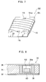
- Fig. 7 is a conceptual view of an IC chip module 132 as a circuit chip module of still another embodiment of the present invention.
- An IC card with IC chip module 132 is substantially similar in appearance and cross section to IC card 100 (shown in Figs. 1 and 2). Furthermore the IC card with IC chip module 132 is also similar in operation to IC card 100.
- IC chip module 132 is comprised of an IC chip 134 serving as a circuit chip, and coil 44 wound around IC chip 134.
- IC chip 134 is substantially similar in configuration to the aforementioned IC chip 114 (shown in Fig. 4), with terminal 119 provided at an upper surface 134a covered with a passivation film. Coil 44 wound around IC chip 134 has an end connected to terminal 119.
- Fig. 8 is a cross section of a non-contact IC card as a circuit chip mounted card of still another embodiment of the present invention.
- IC card 30 is substantially similar in appearance to IC card 100 (shown in Fig. 1).
- IC chip module 102 itself is substantially similarly to that of IC card 100 (shown in Fig. 3).
- IC card 30 is also similar in operation to IC card 100.
- IC card 30 is comprised of surface member 32 corresponding to a first base member, core member 34, and surface member 36 corresponding to a second base member that are deposited successively in the order of appearance above.
- Surface member 32, 36 is formed, e.g., of synthetic resin such as vinyl chloride, polyethylene terephthalate (PET).
- Core member 34 is formed from synthetic resin.
- Ceramic frame 38 is buried in the layer formed of core member 34.
- Ceramic frame 38 is formed of ceramic and has a cylindrical shape.
- Ceramic frame 38 corresponds to a frame of a reinforcement body. In other words, in the present embodiment herein the reinforcement body is constructed only of the frame.
- Ceramic frame 38 has a hollow internal portion 38a. At a lower end of ceramic frame 38 internal portion 38a, a flexible member 40 serving as a buffering member is provided in contact with surface member 32. Flexible member 40 is formed of adhesive silicon rubber. Flexible member 40 supports thereon IC chip module 102 serving as a circuit chip module.
- the reinforcement body formed of ceramic can provide high rigidity.
- ceramic frame 38 buried in the layer formed of core member 34 can remarkably enhance the rigidity of IC card 30 against bending, twisting and pressing forces in a vicinity of ceramic frame 38.
- IC card 30 receives a strong bending, twisting or pressing force or the like, IC chip module 102 arranged in internal portion 38a of the ceramic frame will not deform significantly and will thus hardly be damaged, so that the reliability of IC card 30 can be enhanced.
- surface member 32, 36 is 0.1 mm thick and the entirety of IC card 30 is 0.768 mm thick.
- IC chip module 102 is a cube having a side of 3 mm and a thickness of 0.25 mm.
- Flexible member 40 is 0.118 mm thick.
- Ceramic frame 38 is 0.568 mm high.
- Ceramic frame 38 has an inner diameter set such that the clearance from the incorporated IC chip module 102 is approximately 0.2 to 0.3 mm.
- Ceramic frame 38 also has an outer diameter of approximately 23 mm. It should be noted, however, that the present invention is not limited to the above dimensions or materials.
- IC chip module 102 is fixed to surface member 32 with flexible member 40 interposed therebetween, as shown in Fig. 8, IC chip module 102 may be fixed directly to surface member 32 without flexible member 40 interposed therebetween.
- Fig. 9 is a cross section of a non-contact IC card 50 as a circuit chip mounted card of still another embodiment of the present invention.
- IC card 50 is similar in appearance to IC card 30 (shown in Fig. 1).
- a ceramic frame 52 of IC card 50 is different in shape from ceramic frame 38 (shown in Fig. 8) of IC card 30. More specifically, ceramic frame 38 is constructed only of a cylindrical frame, whereas ceramic frame 52 is comprised of a cylindrical portion 52a as a frame and a bottom 52b in the form of a plate integrated with a lower end of cylindrical portion 52a.
- IC chip module 102 is fixed directly to bottom 52b of a U-shaped space 52c provided by the cylindrical portion 52a and bottom 52b of ceramic frame 52.
- Bottom 52b integrated with the lower end of cylindrical portion 52a allows the rigidity of ceramic frame 52 to be further enhanced.
- a desired rigidity can be ensured if a dimension in the direction of a plane of ceramic frame 52 (the X and Y directions of Fig. 1) is increased to some extent.
- IC chip module 102 can be increased in its dimensions and accordingly coil 44 (shown in Fig. 3) incorporated in IC chip module 102 can further be increased in its dimensions.
- ceramic frame 52 and IC chip module 102 fixed to ceramic frame 52 configure a frame module 54.
- the moduled frame can enhance operability in manufacturing the card and reduce the cost for manufacturing the same.
- IC chip module 102 is fixed directly to ceramic frame 52 bottom 52b
- flexible member 40 as shown in Fig. 8 can be interposed between IC chip module 102 and ceramic frame 52 bottom 52b. Such configuration can conveniently alleviate an impact experienced by the IC card.
- Fig. 12 is a cross section of a non-contact IC card 170 as a circuit chip mounted card of still another embodiment of the present invention.
- IC card 107 is similar in appearance to IC card 30 (shown in Fig. 1).
- IC card 170 ceramic frame 172 in the form of a frame differs in shape from IC card 30 ceramic frame 38 (shown in Fig. 8). More specifically, ceramic frame 172 is externally similar to ceramic frame 38, in the form of a single cylinder, while it is internally in the form of a stepped cylinder and thus different from ceramic frame 38.
- a supporting film 174 serving as a buffering member adheres to a step 172a of ceramic frame 172.
- Supporting film 174 is a synthetic resin film provided in the form of a hollowed disk.
- supporting film 174 is suspended in an internal space 172b of ceramic frame 172, supported by step 172a of ceramic frame 172.
- IC chip module 102 adheres to substantially the center of supporting film 174. Thus, IC chip module 102 is suspended in internal space 172b of ceramic frame 172, supported by supporting film 174.
- the buffering member is not limited in shape or material to the synthetic resin film in the form of a hollowed disk as provided in the present embodiment.
- the reinforcement body is a penetrated cylinder or a bottomed cylinder
- the internal and external shapes of the cylinder are not limited to the aforementioned forms of cylinder.
- the reinforcement body may be a quadratic prism or the like.
- the reinforcement body is also not limited to a cylinder and may, for example, be a flat plate.
- reinforcement bodies can be provided over and under a circuit chip module to sandwich the same.
- the reinforcement body may be formed of any other material than ceramic that has significant rigidity.
- it may be formed of a metal material such as stainless steel, a hard synthetic resin, and the like.
- reinforcement body that reinforces an IC card with IC chip module 102 in the above embodiment is also similarly applicable to an IC card with IC chip module 112 (shown in Fig. 4), 122 (shown in Fig. 6) or 132 (shown in Fig. 7).
- the IC chip module is substantially similar in structure to the Fig. 3 IC chip module 102, although they are different in that the resonance circuit of the Fig. 3 IC chip 104 corresponding to IC chip module 102 is similar to resonance circuit 22 shown in Fig. 14B, whereas the resonance circuit of an IC chip corresponding to the IC chip module of the present embodiment is a resonance circuit 150 shown in Fig. 10.
- Resonance circuit 150 is comprised of a capacitor portion 152 including five capacitors C1 to C5 and five laser taps T1 to T5, and a coil L that are connected as shown in Fig. 10.
- capacitor portion 152 capacitors C1 to C5 are connected in parallel via laser taps T1 to T5 which are conductive and can be cut off by laser radiation.
- any appropriate laser tap T1 to T5 can be cut off to adjust the composite capacitance of capacitor portion 152.
- the adjustment of the composite capacitance of capacitor portion 152 allows a resonance frequency of resonance circuit 150 to be adjusted. It should be noted that laser taps T1 to T5 are cut off in a step subsequent to the contraction of capacitors C1 to C5, coil L and the like in the IC chip.
- resonance frequency can be measured while laser taps T1 to T5 are cut off successively, and the cutting-off of laser taps T1 to T5 can be terminated when the resonance frequency attains a predetermined threshold value.
- an IC chip can be used as a testing sample to find an optimal cutting pattern. Thereafter, for IC chips manufactured in the same process, laser taps T1 to T5 may be cut off in the same pattern.
- the pattern for cutting off laser taps T1 to T5 can be varied for each type of IC chip to set a different resonance frequency for each type of IC chip.
- Capacitors C1 to C5 may have the sane capacitance or may each have a different capacitance.
- capacitors C1 to C5 may be 1 ⁇ F, 2 ⁇ F, 4 ⁇ F, 8 ⁇ F and 16 ⁇ F, respectively, in capacitance. This allows the composite capacitance to be tailored in the range of 1 ⁇ F to 31 ⁇ F by an interval of 1 ⁇ F.
- capacitors and laser taps may be used.
- the Fig. 10 resonance circuit 150 may be substituted by the Fig. 11 resonance circuit 160.
- Resonance circuit 160 is comprised of a coil portion 162 including six coils L1 to L6 and five laser taps T1 to T5, and a capacitor C that are connected as shown in Fig. 11.
- coil portion 162 coils L1 to L6 are connected in series and each connection point between the coils is short-circuited via laser taps T1 to T5.
- Laser taps T1 to T5 can be cut off in ascending order of their numeral references to adjust the composite inductance of coil portion 162.
- the adjustment of the composite inductance of coil portion 162 allows a resonance frequency of resonance circuit 160 to be adjusted. It should be noted that any other number than five of coils and laser taps may be used.
- the resonance circuit with adjustable resonance frequency is not limited to those described above.
- the Fig. 10 resonance circuit 150 and the Fig. 11 resonance circuit 160 can be combined together to construct a resonance circuit.
- the resonance circuit having an adjustable resonance frequency allows the resonance circuit to have capacitance or inductance adjustable after the construction of capacitors and coils in an IC chip.
- the resonance frequency can be adjusted after the circuit elements configuring the resonance circuit are all constructed in the IC chip.
- the resonance frequency can be constant to some extent and an IC card with such an IC chip mounted thereto can be enhanced in reliability. Furthermore an IC chip accommodating a wide range of resonance frequencies can be obtained without changing a masking pattern for forming a circuit element thereof in the process for manufacturing the same, so that the cost for manufacturing the same can be reduced.
- the antenna is not limited to a coil looped as an antenna in each of the above embodiments.
- the antenna may be, e.g., a metal wire in a straight line, a metal wire in the form of a proceeding snake or the like.
- the present invention has been applied to a single-coil, non-contact IC card, the present invention is also applicable to a multiple-coil, non-contact IC card.
- the present invention is also applicable to contact IC cards.
- the present invention is also applicable not only to IC cards but generally to modules and cards with a circuit chip mounted thereto.
- the card referred to herein means generally plate-like members, including credit cards, monthly train tickets, train tickets and the like.
Landscapes
- Engineering & Computer Science (AREA)
- Microelectronics & Electronic Packaging (AREA)
- Computer Hardware Design (AREA)
- Physics & Mathematics (AREA)
- General Physics & Mathematics (AREA)
- Theoretical Computer Science (AREA)
- Computer Networks & Wireless Communication (AREA)
- Credit Cards Or The Like (AREA)
Applications Claiming Priority (3)
| Application Number | Priority Date | Filing Date | Title |
|---|---|---|---|
| JP35138396A JPH10193849A (ja) | 1996-12-27 | 1996-12-27 | 回路チップ搭載カードおよび回路チップモジュール |
| JP35138396 | 1996-12-27 | ||
| PCT/JP1997/004773 WO1998029264A1 (fr) | 1996-12-27 | 1997-12-22 | Carte a puce et module a puce |
Publications (2)
| Publication Number | Publication Date |
|---|---|
| EP1010543A1 true EP1010543A1 (fr) | 2000-06-21 |
| EP1010543A4 EP1010543A4 (fr) | 2005-06-01 |
Family
ID=18416926
Family Applications (1)
| Application Number | Title | Priority Date | Filing Date |
|---|---|---|---|
| EP97949219A Pending EP1010543A4 (fr) | 1996-12-27 | 1997-12-22 | Carte a puce et module a puce |
Country Status (8)
| Country | Link |
|---|---|
| US (1) | US6181001B1 (fr) |
| EP (1) | EP1010543A4 (fr) |
| JP (1) | JPH10193849A (fr) |
| KR (1) | KR100371816B1 (fr) |
| CN (1) | CN1118380C (fr) |
| AU (1) | AU740252B2 (fr) |
| CA (1) | CA2276130A1 (fr) |
| WO (1) | WO1998029264A1 (fr) |
Cited By (92)
| Publication number | Priority date | Publication date | Assignee | Title |
|---|---|---|---|---|
| GB2393685B (en) * | 2001-03-19 | 2005-02-23 | Hitachi Maxell | Core piece and non-contact communication type information carrier using the core piece |
| US7629942B2 (en) | 2006-04-14 | 2009-12-08 | Murata Manufacturing Co., Ltd. | Antenna |
| US7630685B2 (en) | 2006-01-19 | 2009-12-08 | Murata Manufacturing Co., Ltd. | Wireless IC device and component for wireless IC device |
| EP1944829A3 (fr) * | 2006-12-29 | 2010-02-10 | Broadcom Corporation | Structure d'antenne mems à circuit intégré |
| EP1053531B2 (fr) † | 1998-02-04 | 2010-09-29 | Gemalto SA | Dispositif a circuit integre securise par attenuation de signatures electriques |
| US7839334B2 (en) | 2006-12-29 | 2010-11-23 | Broadcom Corporation | IC with a 55-64 GHz antenna |
| US7857230B2 (en) | 2007-07-18 | 2010-12-28 | Murata Manufacturing Co., Ltd. | Wireless IC device and manufacturing method thereof |
| US7894777B1 (en) | 2006-12-29 | 2011-02-22 | Broadcom Corporation | IC with a configurable antenna structure |
| US7893878B2 (en) | 2006-12-29 | 2011-02-22 | Broadcom Corporation | Integrated circuit antenna structure |
| US7931206B2 (en) | 2007-05-10 | 2011-04-26 | Murata Manufacturing Co., Ltd. | Wireless IC device |
| US7944398B2 (en) | 2006-12-29 | 2011-05-17 | Broadcom Corporation | Integrated circuit having a low efficiency antenna |
| US7967216B2 (en) | 2008-05-22 | 2011-06-28 | Murata Manufacturing Co., Ltd. | Wireless IC device |
| US7973730B2 (en) | 2006-12-29 | 2011-07-05 | Broadcom Corporation | Adjustable integrated circuit antenna structure |
| US7979033B2 (en) | 2006-12-29 | 2011-07-12 | Broadcom Corporation | IC antenna structures and applications thereof |
| US7997501B2 (en) | 2007-07-17 | 2011-08-16 | Murata Manufacturing Co., Ltd. | Wireless IC device and electronic apparatus |
| US8011589B2 (en) | 2008-06-25 | 2011-09-06 | Murata Manufacturing Co., Ltd. | Wireless IC device and manufacturing method thereof |
| US8179329B2 (en) | 2008-03-03 | 2012-05-15 | Murata Manufacturing Co., Ltd. | Composite antenna |
| US8177138B2 (en) | 2008-10-29 | 2012-05-15 | Murata Manufacturing Co., Ltd. | Radio IC device |
| US8228765B2 (en) | 2006-06-30 | 2012-07-24 | Murata Manufacturing Co., Ltd. | Optical disc |
| US8299929B2 (en) | 2006-09-26 | 2012-10-30 | Murata Manufacturing Co., Ltd. | Inductively coupled module and item with inductively coupled module |
| US8299968B2 (en) | 2007-02-06 | 2012-10-30 | Murata Manufacturing Co., Ltd. | Packaging material with electromagnetic coupling module |
| US8336786B2 (en) | 2010-03-12 | 2012-12-25 | Murata Manufacturing Co., Ltd. | Wireless communication device and metal article |
| US8342416B2 (en) | 2009-01-09 | 2013-01-01 | Murata Manufacturing Co., Ltd. | Wireless IC device, wireless IC module and method of manufacturing wireless IC module |
| US8360330B2 (en) | 2007-12-26 | 2013-01-29 | Murata Manufacturing Co., Ltd. | Antenna device and radio frequency IC device |
| US8360325B2 (en) | 2008-04-14 | 2013-01-29 | Murata Manufacturing Co., Ltd. | Wireless IC device, electronic apparatus, and method for adjusting resonant frequency of wireless IC device |
| US8360324B2 (en) | 2007-04-09 | 2013-01-29 | Murata Manufacturing Co., Ltd. | Wireless IC device |
| US8381997B2 (en) | 2009-06-03 | 2013-02-26 | Murata Manufacturing Co., Ltd. | Radio frequency IC device and method of manufacturing the same |
| US8390459B2 (en) | 2007-04-06 | 2013-03-05 | Murata Manufacturing Co., Ltd. | Wireless IC device |
| US8400365B2 (en) | 2009-11-20 | 2013-03-19 | Murata Manufacturing Co., Ltd. | Antenna device and mobile communication terminal |
| US8400307B2 (en) | 2007-07-18 | 2013-03-19 | Murata Manufacturing Co., Ltd. | Radio frequency IC device and electronic apparatus |
| US8418928B2 (en) | 2009-04-14 | 2013-04-16 | Murata Manufacturing Co., Ltd. | Wireless IC device component and wireless IC device |
| US8424762B2 (en) | 2007-04-14 | 2013-04-23 | Murata Manufacturing Co., Ltd. | Wireless IC device and component for wireless IC device |
| US8424769B2 (en) | 2010-07-08 | 2013-04-23 | Murata Manufacturing Co., Ltd. | Antenna and RFID device |
| US8474725B2 (en) | 2007-04-27 | 2013-07-02 | Murata Manufacturing Co., Ltd. | Wireless IC device |
| US8531346B2 (en) | 2007-04-26 | 2013-09-10 | Murata Manufacturing Co., Ltd. | Wireless IC device |
| US8546927B2 (en) | 2010-09-03 | 2013-10-01 | Murata Manufacturing Co., Ltd. | RFIC chip mounting structure |
| US8552870B2 (en) | 2007-07-09 | 2013-10-08 | Murata Manufacturing Co., Ltd. | Wireless IC device |
| US8583043B2 (en) | 2009-01-16 | 2013-11-12 | Murata Manufacturing Co., Ltd. | High-frequency device and wireless IC device |
| US8590797B2 (en) | 2008-05-21 | 2013-11-26 | Murata Manufacturing Co., Ltd. | Wireless IC device |
| US8596545B2 (en) | 2008-05-28 | 2013-12-03 | Murata Manufacturing Co., Ltd. | Component of wireless IC device and wireless IC device |
| US8602310B2 (en) | 2010-03-03 | 2013-12-10 | Murata Manufacturing Co., Ltd. | Radio communication device and radio communication terminal |
| US8610636B2 (en) | 2007-12-20 | 2013-12-17 | Murata Manufacturing Co., Ltd. | Radio frequency IC device |
| US8613395B2 (en) | 2011-02-28 | 2013-12-24 | Murata Manufacturing Co., Ltd. | Wireless communication device |
| US8632014B2 (en) | 2007-04-27 | 2014-01-21 | Murata Manufacturing Co., Ltd. | Wireless IC device |
| US8668151B2 (en) | 2008-03-26 | 2014-03-11 | Murata Manufacturing Co., Ltd. | Wireless IC device |
| US8680971B2 (en) | 2009-09-28 | 2014-03-25 | Murata Manufacturing Co., Ltd. | Wireless IC device and method of detecting environmental state using the device |
| US8692718B2 (en) | 2008-11-17 | 2014-04-08 | Murata Manufacturing Co., Ltd. | Antenna and wireless IC device |
| US8718727B2 (en) | 2009-12-24 | 2014-05-06 | Murata Manufacturing Co., Ltd. | Antenna having structure for multi-angled reception and mobile terminal including the antenna |
| US8720789B2 (en) | 2012-01-30 | 2014-05-13 | Murata Manufacturing Co., Ltd. | Wireless IC device |
| US8740093B2 (en) | 2011-04-13 | 2014-06-03 | Murata Manufacturing Co., Ltd. | Radio IC device and radio communication terminal |
| US8757500B2 (en) | 2007-05-11 | 2014-06-24 | Murata Manufacturing Co., Ltd. | Wireless IC device |
| US8770489B2 (en) | 2011-07-15 | 2014-07-08 | Murata Manufacturing Co., Ltd. | Radio communication device |
| US8797148B2 (en) | 2008-03-03 | 2014-08-05 | Murata Manufacturing Co., Ltd. | Radio frequency IC device and radio communication system |
| US8797225B2 (en) | 2011-03-08 | 2014-08-05 | Murata Manufacturing Co., Ltd. | Antenna device and communication terminal apparatus |
| US8810456B2 (en) | 2009-06-19 | 2014-08-19 | Murata Manufacturing Co., Ltd. | Wireless IC device and coupling method for power feeding circuit and radiation plate |
| US8814056B2 (en) | 2011-07-19 | 2014-08-26 | Murata Manufacturing Co., Ltd. | Antenna device, RFID tag, and communication terminal apparatus |
| US8853549B2 (en) | 2009-09-30 | 2014-10-07 | Murata Manufacturing Co., Ltd. | Circuit substrate and method of manufacturing same |
| US8870077B2 (en) | 2008-08-19 | 2014-10-28 | Murata Manufacturing Co., Ltd. | Wireless IC device and method for manufacturing same |
| US8878739B2 (en) | 2011-07-14 | 2014-11-04 | Murata Manufacturing Co., Ltd. | Wireless communication device |
| US8905316B2 (en) | 2010-05-14 | 2014-12-09 | Murata Manufacturing Co., Ltd. | Wireless IC device |
| US8905296B2 (en) | 2011-12-01 | 2014-12-09 | Murata Manufacturing Co., Ltd. | Wireless integrated circuit device and method of manufacturing the same |
| US8937576B2 (en) | 2011-04-05 | 2015-01-20 | Murata Manufacturing Co., Ltd. | Wireless communication device |
| US8944335B2 (en) | 2010-09-30 | 2015-02-03 | Murata Manufacturing Co., Ltd. | Wireless IC device |
| US8976075B2 (en) | 2009-04-21 | 2015-03-10 | Murata Manufacturing Co., Ltd. | Antenna device and method of setting resonant frequency of antenna device |
| US8981906B2 (en) | 2010-08-10 | 2015-03-17 | Murata Manufacturing Co., Ltd. | Printed wiring board and wireless communication system |
| US8991713B2 (en) | 2011-01-14 | 2015-03-31 | Murata Manufacturing Co., Ltd. | RFID chip package and RFID tag |
| US8994605B2 (en) | 2009-10-02 | 2015-03-31 | Murata Manufacturing Co., Ltd. | Wireless IC device and electromagnetic coupling module |
| US9024725B2 (en) | 2009-11-04 | 2015-05-05 | Murata Manufacturing Co., Ltd. | Communication terminal and information processing system |
| US9024837B2 (en) | 2010-03-31 | 2015-05-05 | Murata Manufacturing Co., Ltd. | Antenna and wireless communication device |
| US9077067B2 (en) | 2008-07-04 | 2015-07-07 | Murata Manufacturing Co., Ltd. | Radio IC device |
| US9104950B2 (en) | 2009-01-30 | 2015-08-11 | Murata Manufacturing Co., Ltd. | Antenna and wireless IC device |
| US9123996B2 (en) | 2010-05-14 | 2015-09-01 | Murata Manufacturing Co., Ltd. | Wireless IC device |
| EP2926298A1 (fr) * | 2012-11-27 | 2015-10-07 | Gemalto SA | Module electronique a interface de communication tridimensionnelle |
| US9166291B2 (en) | 2010-10-12 | 2015-10-20 | Murata Manufacturing Co., Ltd. | Antenna device and communication terminal apparatus |
| US9165239B2 (en) | 2006-04-26 | 2015-10-20 | Murata Manufacturing Co., Ltd. | Electromagnetic-coupling-module-attached article |
| US9178279B2 (en) | 2009-11-04 | 2015-11-03 | Murata Manufacturing Co., Ltd. | Wireless IC tag, reader-writer, and information processing system |
| US9231305B2 (en) | 2008-10-24 | 2016-01-05 | Murata Manufacturing Co., Ltd. | Wireless IC device |
| US9236651B2 (en) | 2010-10-21 | 2016-01-12 | Murata Manufacturing Co., Ltd. | Communication terminal device |
| US9281873B2 (en) | 2008-05-26 | 2016-03-08 | Murata Manufacturing Co., Ltd. | Wireless IC device system and method of determining authenticity of wireless IC device |
| US9378452B2 (en) | 2011-05-16 | 2016-06-28 | Murata Manufacturing Co., Ltd. | Radio IC device |
| US9444143B2 (en) | 2009-10-16 | 2016-09-13 | Murata Manufacturing Co., Ltd. | Antenna and wireless IC device |
| US9460376B2 (en) | 2007-07-18 | 2016-10-04 | Murata Manufacturing Co., Ltd. | Radio IC device |
| US9460320B2 (en) | 2009-10-27 | 2016-10-04 | Murata Manufacturing Co., Ltd. | Transceiver and radio frequency identification tag reader |
| US9461363B2 (en) | 2009-11-04 | 2016-10-04 | Murata Manufacturing Co., Ltd. | Communication terminal and information processing system |
| US9543642B2 (en) | 2011-09-09 | 2017-01-10 | Murata Manufacturing Co., Ltd. | Antenna device and wireless device |
| US9558384B2 (en) | 2010-07-28 | 2017-01-31 | Murata Manufacturing Co., Ltd. | Antenna apparatus and communication terminal instrument |
| EP3182336A1 (fr) * | 2015-12-14 | 2017-06-21 | Gemalto Sa | Dispositif radiofrequence a circuit lc ajustable comprenant un module electrique et/ou electronique |
| US9692128B2 (en) | 2012-02-24 | 2017-06-27 | Murata Manufacturing Co., Ltd. | Antenna device and wireless communication device |
| US9727765B2 (en) | 2010-03-24 | 2017-08-08 | Murata Manufacturing Co., Ltd. | RFID system including a reader/writer and RFID tag |
| US9761923B2 (en) | 2011-01-05 | 2017-09-12 | Murata Manufacturing Co., Ltd. | Wireless communication device |
| US10013650B2 (en) | 2010-03-03 | 2018-07-03 | Murata Manufacturing Co., Ltd. | Wireless communication module and wireless communication device |
| US10235544B2 (en) | 2012-04-13 | 2019-03-19 | Murata Manufacturing Co., Ltd. | Inspection method and inspection device for RFID tag |
Families Citing this family (33)
| Publication number | Priority date | Publication date | Assignee | Title |
|---|---|---|---|---|
| FR2782821B1 (fr) * | 1998-08-27 | 2001-10-12 | Gemplus Card Int | Procede de fabrication de carte a puce sans contact |
| TW484101B (en) * | 1998-12-17 | 2002-04-21 | Hitachi Ltd | Semiconductor device and its manufacturing method |
| JP4589375B2 (ja) * | 1998-12-17 | 2010-12-01 | 株式会社日立製作所 | 半導体装置 |
| US6373447B1 (en) * | 1998-12-28 | 2002-04-16 | Kawasaki Steel Corporation | On-chip antenna, and systems utilizing same |
| EP1455302B1 (fr) * | 1999-02-24 | 2007-09-19 | Hitachi Maxell, Ltd. | Procédé de produire des circuits intégrés comportant une bobine |
| JP2001005942A (ja) * | 1999-06-24 | 2001-01-12 | Shinko Electric Ind Co Ltd | Icカード及びその製造方法並びにアンテナ付き半導体装置及びその製造方法 |
| JP3513452B2 (ja) * | 1999-07-02 | 2004-03-31 | 新光電気工業株式会社 | 非接触型icカードと非接触型icカードの製造方法と非接触型icカード用平面コイル |
| US6486853B2 (en) * | 2000-05-18 | 2002-11-26 | Matsushita Electric Industrial Co., Ltd. | Chip antenna, radio communications terminal and radio communications system using the same and method for production of the same |
| JP4705726B2 (ja) * | 2000-10-23 | 2011-06-22 | 日立マクセル株式会社 | 非接触通信式情報担体用コアピース |
| EP1350233A4 (fr) * | 2000-12-15 | 2005-04-13 | Electrox Corp | Procede de fabrication de nouveaux dispositifs d'identification par frequence radio a bas prix |
| JP4839510B2 (ja) * | 2001-01-17 | 2011-12-21 | 大日本印刷株式会社 | カード基体、icカード及びその製造方法 |
| JP4690561B2 (ja) * | 2001-01-24 | 2011-06-01 | 日立マクセル株式会社 | 半導体チップ |
| US6967347B2 (en) * | 2001-05-21 | 2005-11-22 | The Regents Of The University Of Colorado | Terahertz interconnect system and applications |
| US6563185B2 (en) * | 2001-05-21 | 2003-05-13 | The Regents Of The University Of Colorado | High speed electron tunneling device and applications |
| US7177515B2 (en) | 2002-03-20 | 2007-02-13 | The Regents Of The University Of Colorado | Surface plasmon devices |
| US7126151B2 (en) * | 2001-05-21 | 2006-10-24 | The Regents Of The University Of Colorado, A Body Corporate | Interconnected high speed electron tunneling devices |
| JP4759174B2 (ja) * | 2001-07-10 | 2011-08-31 | 日立マクセル株式会社 | 非接触通信式情報担体 |
| JP2003317052A (ja) * | 2002-04-24 | 2003-11-07 | Smart Card:Kk | Icタグシステム |
| US7042418B2 (en) * | 2002-11-27 | 2006-05-09 | Matsushita Electric Industrial Co., Ltd. | Chip antenna |
| EP1593181A2 (fr) * | 2003-04-10 | 2005-11-09 | Matsushita Electric Industrial Co., Ltd. | Element d'antenne et module d'antenne, et equipement les utilisant |
| US20050013106A1 (en) * | 2003-07-17 | 2005-01-20 | Takiar Hem P. | Peripheral card with hidden test pins |
| WO2005022688A1 (fr) * | 2003-09-01 | 2005-03-10 | Matsushita Electric Industrial Co., Ltd. | Module d'antenne |
| JP2005093867A (ja) * | 2003-09-19 | 2005-04-07 | Seiko Epson Corp | 半導体装置及びその製造方法 |
| JP2005175757A (ja) * | 2003-12-10 | 2005-06-30 | Matsushita Electric Ind Co Ltd | アンテナモジュール |
| KR100934429B1 (ko) * | 2005-05-24 | 2009-12-29 | 후지쯔 가부시끼가이샤 | Ic 태그의 실장 구조 및 실장용 ic 칩 |
| JP5155616B2 (ja) * | 2007-07-25 | 2013-03-06 | 沖プリンテッドサーキット株式会社 | Rfidタグ、rfidシステムおよびrfidタグの製造方法 |
| KR100862890B1 (ko) | 2008-03-07 | 2008-10-13 | 산양전기주식회사 | Rfid 안테나 회로 장치 및 이를 포함하는 rfid카드 |
| DE102010039156A1 (de) * | 2010-08-10 | 2012-02-16 | Robert Bosch Gmbh | Verfahren zum Herstellen einer elektrischen Schaltung und elektrische Schaltung |
| JP6163807B2 (ja) * | 2013-03-21 | 2017-07-19 | 凸版印刷株式会社 | 封緘鍵の製造方法 |
| EP3073573A4 (fr) * | 2013-11-18 | 2017-06-21 | Ricoh Company, Ltd. | Procédé de fabrication d'antenne bobine et procédé de fabrication de corps de montage d'antenne bobine |
| CN103762418A (zh) * | 2014-01-09 | 2014-04-30 | 东莞晶汇半导体有限公司 | 天线溅镀在射频模组表面上工艺 |
| US10461396B2 (en) * | 2015-04-03 | 2019-10-29 | Fit Pay, Inc. | System and method for low-power close-proximity communications and energy transfer using a miniature multi-purpose antenna |
| DE102020118575B4 (de) * | 2020-07-14 | 2022-03-03 | Infineon Technologies Ag | Nahfeldkommunikationsvorrichtung, elektronische Vorrichtung zum Bereitstellen einer Substanz, Verfahren zum Betreiben einer Nahfeldkommunikationsvorrichtung und Verfahren zum Bereitstellen einer Substanz |
Family Cites Families (22)
| Publication number | Priority date | Publication date | Assignee | Title |
|---|---|---|---|---|
| DE3721822C1 (en) * | 1987-07-02 | 1988-11-10 | Philips Patentverwaltung | Chip card |
| US5153583A (en) * | 1987-11-18 | 1992-10-06 | Uniscan Ltd. | Transponder |
| JP2549192B2 (ja) | 1990-09-19 | 1996-10-30 | 三菱電機株式会社 | 非接触icカード及びその使用方法 |
| DE4034225C2 (de) * | 1990-10-26 | 1994-01-27 | Reinhard Jurisch | Datenträger für Identifikationssysteme |
| JPH04260990A (ja) | 1991-01-25 | 1992-09-16 | Mitsubishi Electric Corp | 非接触icカード |
| JPH05250529A (ja) * | 1992-03-04 | 1993-09-28 | Fuji Electric Co Ltd | Icモジュール |
| FR2691563B1 (fr) * | 1992-05-19 | 1996-05-31 | Francois Droz | Carte comprenant au moins un element electronique et procede de fabrication d'une telle carte. |
| DE4311493C2 (de) * | 1993-04-07 | 2000-04-06 | Amatech Advanced Micromechanic | IC-Kartenmodul zur Herstellung einer IC-Karte |
| NL9301457A (nl) * | 1993-08-23 | 1995-03-16 | Nedap Nv | Contactloze identificatiekaart of smart card. |
| US5541604A (en) * | 1993-09-03 | 1996-07-30 | Texas Instruments Deutschland Gmbh | Transponders, Interrogators, systems and methods for elimination of interrogator synchronization requirement |
| JP3305843B2 (ja) * | 1993-12-20 | 2002-07-24 | 株式会社東芝 | 半導体装置 |
| JP3259499B2 (ja) | 1993-12-28 | 2002-02-25 | オムロン株式会社 | 電子カード |
| FR2716281B1 (fr) * | 1994-02-14 | 1996-05-03 | Gemplus Card Int | Procédé de fabrication d'une carte sans contact. |
| FR2716555B1 (fr) * | 1994-02-24 | 1996-05-15 | Gemplus Card Int | Procédé de fabrication d'une carte sans contact. |
| JP3097444B2 (ja) * | 1994-03-31 | 2000-10-10 | 株式会社村田製作所 | 電圧制御形発振器の発振周波数可変範囲調整方法 |
| JPH0822582A (ja) * | 1994-07-06 | 1996-01-23 | Toyo Alum Kk | 共鳴ラベル |
| JPH08282167A (ja) | 1995-04-13 | 1996-10-29 | Rohm Co Ltd | Icカード |
| FR2727541B1 (fr) * | 1994-11-25 | 1997-01-17 | Droz Francois | Carte incorporant au moins une bobine |
| JP2814477B2 (ja) * | 1995-04-13 | 1998-10-22 | ソニーケミカル株式会社 | 非接触式icカード及びその製造方法 |
| JP3092693B2 (ja) * | 1995-05-26 | 2000-09-25 | ティーディーケイ株式会社 | 複合電子部品 |
| FR2747812B1 (fr) * | 1996-04-23 | 1998-05-22 | Solaic Sa | Carte a circuit integre sans contact avec antenne en polymere conducteur |
| US6049463A (en) * | 1997-07-25 | 2000-04-11 | Motorola, Inc. | Microelectronic assembly including an antenna element embedded within a polymeric card, and method for forming same |
-
1996
- 1996-12-27 JP JP35138396A patent/JPH10193849A/ja active Pending
-
1997
- 1997-12-22 US US09/331,191 patent/US6181001B1/en not_active Expired - Lifetime
- 1997-12-22 CA CA002276130A patent/CA2276130A1/fr not_active Abandoned
- 1997-12-22 KR KR10-1999-7005778A patent/KR100371816B1/ko not_active Expired - Fee Related
- 1997-12-22 AU AU78896/98A patent/AU740252B2/en not_active Ceased
- 1997-12-22 EP EP97949219A patent/EP1010543A4/fr active Pending
- 1997-12-22 CN CN97181556A patent/CN1118380C/zh not_active Expired - Fee Related
- 1997-12-22 WO PCT/JP1997/004773 patent/WO1998029264A1/fr not_active Ceased
Cited By (122)
| Publication number | Priority date | Publication date | Assignee | Title |
|---|---|---|---|---|
| EP1053531B2 (fr) † | 1998-02-04 | 2010-09-29 | Gemalto SA | Dispositif a circuit integre securise par attenuation de signatures electriques |
| GB2393685B (en) * | 2001-03-19 | 2005-02-23 | Hitachi Maxell | Core piece and non-contact communication type information carrier using the core piece |
| US7159785B2 (en) | 2001-03-19 | 2007-01-09 | Hitachi Maxell, Ltd. | Core piece and non-contact communication type information carrier using the core piece |
| DE10296526B4 (de) * | 2001-03-19 | 2008-11-13 | Hitachi Maxell, Ltd., Ibaraki | Kernstück und das Kernstück verwendender Informationsträger für berührungslose Kommunikation |
| US8725071B2 (en) | 2006-01-19 | 2014-05-13 | Murata Manufacturing Co., Ltd. | Wireless IC device and component for wireless IC device |
| US7630685B2 (en) | 2006-01-19 | 2009-12-08 | Murata Manufacturing Co., Ltd. | Wireless IC device and component for wireless IC device |
| US8078106B2 (en) | 2006-01-19 | 2011-12-13 | Murata Manufacturing Co., Ltd. | Wireless IC device and component for wireless IC device |
| US8676117B2 (en) | 2006-01-19 | 2014-03-18 | Murata Manufacturing Co., Ltd. | Wireless IC device and component for wireless IC device |
| US8326223B2 (en) | 2006-01-19 | 2012-12-04 | Murata Manufacturing Co., Ltd. | Wireless IC device and component for wireless IC device |
| US7629942B2 (en) | 2006-04-14 | 2009-12-08 | Murata Manufacturing Co., Ltd. | Antenna |
| US9165239B2 (en) | 2006-04-26 | 2015-10-20 | Murata Manufacturing Co., Ltd. | Electromagnetic-coupling-module-attached article |
| US8228765B2 (en) | 2006-06-30 | 2012-07-24 | Murata Manufacturing Co., Ltd. | Optical disc |
| US8299929B2 (en) | 2006-09-26 | 2012-10-30 | Murata Manufacturing Co., Ltd. | Inductively coupled module and item with inductively coupled module |
| KR101024047B1 (ko) * | 2006-12-29 | 2011-03-22 | 브로드콤 코포레이션 | 집적회로 mems 안테나 구조체 |
| US8193991B2 (en) | 2006-12-29 | 2012-06-05 | Broadcom Corporation | Integrated circuit MEMS antenna structure |
| US7973730B2 (en) | 2006-12-29 | 2011-07-05 | Broadcom Corporation | Adjustable integrated circuit antenna structure |
| US7979033B2 (en) | 2006-12-29 | 2011-07-12 | Broadcom Corporation | IC antenna structures and applications thereof |
| US7944398B2 (en) | 2006-12-29 | 2011-05-17 | Broadcom Corporation | Integrated circuit having a low efficiency antenna |
| US7894777B1 (en) | 2006-12-29 | 2011-02-22 | Broadcom Corporation | IC with a configurable antenna structure |
| US8232919B2 (en) | 2006-12-29 | 2012-07-31 | Broadcom Corporation | Integrated circuit MEMs antenna structure |
| US7893878B2 (en) | 2006-12-29 | 2011-02-22 | Broadcom Corporation | Integrated circuit antenna structure |
| US7839334B2 (en) | 2006-12-29 | 2010-11-23 | Broadcom Corporation | IC with a 55-64 GHz antenna |
| EP1944829A3 (fr) * | 2006-12-29 | 2010-02-10 | Broadcom Corporation | Structure d'antenne mems à circuit intégré |
| US8299968B2 (en) | 2007-02-06 | 2012-10-30 | Murata Manufacturing Co., Ltd. | Packaging material with electromagnetic coupling module |
| US8390459B2 (en) | 2007-04-06 | 2013-03-05 | Murata Manufacturing Co., Ltd. | Wireless IC device |
| US8360324B2 (en) | 2007-04-09 | 2013-01-29 | Murata Manufacturing Co., Ltd. | Wireless IC device |
| US8424762B2 (en) | 2007-04-14 | 2013-04-23 | Murata Manufacturing Co., Ltd. | Wireless IC device and component for wireless IC device |
| US8531346B2 (en) | 2007-04-26 | 2013-09-10 | Murata Manufacturing Co., Ltd. | Wireless IC device |
| US8632014B2 (en) | 2007-04-27 | 2014-01-21 | Murata Manufacturing Co., Ltd. | Wireless IC device |
| US8474725B2 (en) | 2007-04-27 | 2013-07-02 | Murata Manufacturing Co., Ltd. | Wireless IC device |
| US7931206B2 (en) | 2007-05-10 | 2011-04-26 | Murata Manufacturing Co., Ltd. | Wireless IC device |
| US8757500B2 (en) | 2007-05-11 | 2014-06-24 | Murata Manufacturing Co., Ltd. | Wireless IC device |
| US8662403B2 (en) | 2007-07-04 | 2014-03-04 | Murata Manufacturing Co., Ltd. | Wireless IC device and component for wireless IC device |
| US8552870B2 (en) | 2007-07-09 | 2013-10-08 | Murata Manufacturing Co., Ltd. | Wireless IC device |
| US8191791B2 (en) | 2007-07-17 | 2012-06-05 | Murata Manufacturing Co., Ltd. | Wireless IC device and electronic apparatus |
| US8413907B2 (en) | 2007-07-17 | 2013-04-09 | Murata Manufacturing Co., Ltd. | Wireless IC device and electronic apparatus |
| US7997501B2 (en) | 2007-07-17 | 2011-08-16 | Murata Manufacturing Co., Ltd. | Wireless IC device and electronic apparatus |
| US9830552B2 (en) | 2007-07-18 | 2017-11-28 | Murata Manufacturing Co., Ltd. | Radio IC device |
| US8400307B2 (en) | 2007-07-18 | 2013-03-19 | Murata Manufacturing Co., Ltd. | Radio frequency IC device and electronic apparatus |
| US9460376B2 (en) | 2007-07-18 | 2016-10-04 | Murata Manufacturing Co., Ltd. | Radio IC device |
| US7857230B2 (en) | 2007-07-18 | 2010-12-28 | Murata Manufacturing Co., Ltd. | Wireless IC device and manufacturing method thereof |
| US8610636B2 (en) | 2007-12-20 | 2013-12-17 | Murata Manufacturing Co., Ltd. | Radio frequency IC device |
| US8360330B2 (en) | 2007-12-26 | 2013-01-29 | Murata Manufacturing Co., Ltd. | Antenna device and radio frequency IC device |
| US8915448B2 (en) | 2007-12-26 | 2014-12-23 | Murata Manufacturing Co., Ltd. | Antenna device and radio frequency IC device |
| US8797148B2 (en) | 2008-03-03 | 2014-08-05 | Murata Manufacturing Co., Ltd. | Radio frequency IC device and radio communication system |
| US8179329B2 (en) | 2008-03-03 | 2012-05-15 | Murata Manufacturing Co., Ltd. | Composite antenna |
| US8668151B2 (en) | 2008-03-26 | 2014-03-11 | Murata Manufacturing Co., Ltd. | Wireless IC device |
| US8360325B2 (en) | 2008-04-14 | 2013-01-29 | Murata Manufacturing Co., Ltd. | Wireless IC device, electronic apparatus, and method for adjusting resonant frequency of wireless IC device |
| US8960557B2 (en) | 2008-05-21 | 2015-02-24 | Murata Manufacturing Co., Ltd. | Wireless IC device |
| US8590797B2 (en) | 2008-05-21 | 2013-11-26 | Murata Manufacturing Co., Ltd. | Wireless IC device |
| US9022295B2 (en) | 2008-05-21 | 2015-05-05 | Murata Manufacturing Co., Ltd. | Wireless IC device |
| US8973841B2 (en) | 2008-05-21 | 2015-03-10 | Murata Manufacturing Co., Ltd. | Wireless IC device |
| US7967216B2 (en) | 2008-05-22 | 2011-06-28 | Murata Manufacturing Co., Ltd. | Wireless IC device |
| US8047445B2 (en) | 2008-05-22 | 2011-11-01 | Murata Manufacturing Co., Ltd. | Wireless IC device and method of manufacturing the same |
| US9281873B2 (en) | 2008-05-26 | 2016-03-08 | Murata Manufacturing Co., Ltd. | Wireless IC device system and method of determining authenticity of wireless IC device |
| US8596545B2 (en) | 2008-05-28 | 2013-12-03 | Murata Manufacturing Co., Ltd. | Component of wireless IC device and wireless IC device |
| US8011589B2 (en) | 2008-06-25 | 2011-09-06 | Murata Manufacturing Co., Ltd. | Wireless IC device and manufacturing method thereof |
| US9077067B2 (en) | 2008-07-04 | 2015-07-07 | Murata Manufacturing Co., Ltd. | Radio IC device |
| US8870077B2 (en) | 2008-08-19 | 2014-10-28 | Murata Manufacturing Co., Ltd. | Wireless IC device and method for manufacturing same |
| US9231305B2 (en) | 2008-10-24 | 2016-01-05 | Murata Manufacturing Co., Ltd. | Wireless IC device |
| US8177138B2 (en) | 2008-10-29 | 2012-05-15 | Murata Manufacturing Co., Ltd. | Radio IC device |
| US8692718B2 (en) | 2008-11-17 | 2014-04-08 | Murata Manufacturing Co., Ltd. | Antenna and wireless IC device |
| US8917211B2 (en) | 2008-11-17 | 2014-12-23 | Murata Manufacturing Co., Ltd. | Antenna and wireless IC device |
| US8342416B2 (en) | 2009-01-09 | 2013-01-01 | Murata Manufacturing Co., Ltd. | Wireless IC device, wireless IC module and method of manufacturing wireless IC module |
| US8544759B2 (en) | 2009-01-09 | 2013-10-01 | Murata Manufacturing., Ltd. | Wireless IC device, wireless IC module and method of manufacturing wireless IC module |
| US8583043B2 (en) | 2009-01-16 | 2013-11-12 | Murata Manufacturing Co., Ltd. | High-frequency device and wireless IC device |
| US9104950B2 (en) | 2009-01-30 | 2015-08-11 | Murata Manufacturing Co., Ltd. | Antenna and wireless IC device |
| US8690070B2 (en) | 2009-04-14 | 2014-04-08 | Murata Manufacturing Co., Ltd. | Wireless IC device component and wireless IC device |
| US8418928B2 (en) | 2009-04-14 | 2013-04-16 | Murata Manufacturing Co., Ltd. | Wireless IC device component and wireless IC device |
| US8876010B2 (en) | 2009-04-14 | 2014-11-04 | Murata Manufacturing Co., Ltd | Wireless IC device component and wireless IC device |
| US9564678B2 (en) | 2009-04-21 | 2017-02-07 | Murata Manufacturing Co., Ltd. | Antenna device and method of setting resonant frequency of antenna device |
| US8976075B2 (en) | 2009-04-21 | 2015-03-10 | Murata Manufacturing Co., Ltd. | Antenna device and method of setting resonant frequency of antenna device |
| US9203157B2 (en) | 2009-04-21 | 2015-12-01 | Murata Manufacturing Co., Ltd. | Antenna device and method of setting resonant frequency of antenna device |
| US8381997B2 (en) | 2009-06-03 | 2013-02-26 | Murata Manufacturing Co., Ltd. | Radio frequency IC device and method of manufacturing the same |
| US8810456B2 (en) | 2009-06-19 | 2014-08-19 | Murata Manufacturing Co., Ltd. | Wireless IC device and coupling method for power feeding circuit and radiation plate |
| US8680971B2 (en) | 2009-09-28 | 2014-03-25 | Murata Manufacturing Co., Ltd. | Wireless IC device and method of detecting environmental state using the device |
| US8853549B2 (en) | 2009-09-30 | 2014-10-07 | Murata Manufacturing Co., Ltd. | Circuit substrate and method of manufacturing same |
| US9117157B2 (en) | 2009-10-02 | 2015-08-25 | Murata Manufacturing Co., Ltd. | Wireless IC device and electromagnetic coupling module |
| US8994605B2 (en) | 2009-10-02 | 2015-03-31 | Murata Manufacturing Co., Ltd. | Wireless IC device and electromagnetic coupling module |
| US9444143B2 (en) | 2009-10-16 | 2016-09-13 | Murata Manufacturing Co., Ltd. | Antenna and wireless IC device |
| US9460320B2 (en) | 2009-10-27 | 2016-10-04 | Murata Manufacturing Co., Ltd. | Transceiver and radio frequency identification tag reader |
| US9178279B2 (en) | 2009-11-04 | 2015-11-03 | Murata Manufacturing Co., Ltd. | Wireless IC tag, reader-writer, and information processing system |
| US9024725B2 (en) | 2009-11-04 | 2015-05-05 | Murata Manufacturing Co., Ltd. | Communication terminal and information processing system |
| US9461363B2 (en) | 2009-11-04 | 2016-10-04 | Murata Manufacturing Co., Ltd. | Communication terminal and information processing system |
| US8704716B2 (en) | 2009-11-20 | 2014-04-22 | Murata Manufacturing Co., Ltd. | Antenna device and mobile communication terminal |
| US8400365B2 (en) | 2009-11-20 | 2013-03-19 | Murata Manufacturing Co., Ltd. | Antenna device and mobile communication terminal |
| US8718727B2 (en) | 2009-12-24 | 2014-05-06 | Murata Manufacturing Co., Ltd. | Antenna having structure for multi-angled reception and mobile terminal including the antenna |
| US10013650B2 (en) | 2010-03-03 | 2018-07-03 | Murata Manufacturing Co., Ltd. | Wireless communication module and wireless communication device |
| US8602310B2 (en) | 2010-03-03 | 2013-12-10 | Murata Manufacturing Co., Ltd. | Radio communication device and radio communication terminal |
| US8336786B2 (en) | 2010-03-12 | 2012-12-25 | Murata Manufacturing Co., Ltd. | Wireless communication device and metal article |
| US8528829B2 (en) | 2010-03-12 | 2013-09-10 | Murata Manufacturing Co., Ltd. | Wireless communication device and metal article |
| US9727765B2 (en) | 2010-03-24 | 2017-08-08 | Murata Manufacturing Co., Ltd. | RFID system including a reader/writer and RFID tag |
| US9024837B2 (en) | 2010-03-31 | 2015-05-05 | Murata Manufacturing Co., Ltd. | Antenna and wireless communication device |
| US8905316B2 (en) | 2010-05-14 | 2014-12-09 | Murata Manufacturing Co., Ltd. | Wireless IC device |
| US9123996B2 (en) | 2010-05-14 | 2015-09-01 | Murata Manufacturing Co., Ltd. | Wireless IC device |
| US8424769B2 (en) | 2010-07-08 | 2013-04-23 | Murata Manufacturing Co., Ltd. | Antenna and RFID device |
| US9558384B2 (en) | 2010-07-28 | 2017-01-31 | Murata Manufacturing Co., Ltd. | Antenna apparatus and communication terminal instrument |
| US8981906B2 (en) | 2010-08-10 | 2015-03-17 | Murata Manufacturing Co., Ltd. | Printed wiring board and wireless communication system |
| US8546927B2 (en) | 2010-09-03 | 2013-10-01 | Murata Manufacturing Co., Ltd. | RFIC chip mounting structure |
| US8944335B2 (en) | 2010-09-30 | 2015-02-03 | Murata Manufacturing Co., Ltd. | Wireless IC device |
| US9166291B2 (en) | 2010-10-12 | 2015-10-20 | Murata Manufacturing Co., Ltd. | Antenna device and communication terminal apparatus |
| US9236651B2 (en) | 2010-10-21 | 2016-01-12 | Murata Manufacturing Co., Ltd. | Communication terminal device |
| US9761923B2 (en) | 2011-01-05 | 2017-09-12 | Murata Manufacturing Co., Ltd. | Wireless communication device |
| US8991713B2 (en) | 2011-01-14 | 2015-03-31 | Murata Manufacturing Co., Ltd. | RFID chip package and RFID tag |
| US8613395B2 (en) | 2011-02-28 | 2013-12-24 | Murata Manufacturing Co., Ltd. | Wireless communication device |
| US8757502B2 (en) | 2011-02-28 | 2014-06-24 | Murata Manufacturing Co., Ltd. | Wireless communication device |
| US8960561B2 (en) | 2011-02-28 | 2015-02-24 | Murata Manufacturing Co., Ltd. | Wireless communication device |
| US8797225B2 (en) | 2011-03-08 | 2014-08-05 | Murata Manufacturing Co., Ltd. | Antenna device and communication terminal apparatus |
| US8937576B2 (en) | 2011-04-05 | 2015-01-20 | Murata Manufacturing Co., Ltd. | Wireless communication device |
| US8740093B2 (en) | 2011-04-13 | 2014-06-03 | Murata Manufacturing Co., Ltd. | Radio IC device and radio communication terminal |
| US9378452B2 (en) | 2011-05-16 | 2016-06-28 | Murata Manufacturing Co., Ltd. | Radio IC device |
| US8878739B2 (en) | 2011-07-14 | 2014-11-04 | Murata Manufacturing Co., Ltd. | Wireless communication device |
| US8770489B2 (en) | 2011-07-15 | 2014-07-08 | Murata Manufacturing Co., Ltd. | Radio communication device |
| US8814056B2 (en) | 2011-07-19 | 2014-08-26 | Murata Manufacturing Co., Ltd. | Antenna device, RFID tag, and communication terminal apparatus |
| US9543642B2 (en) | 2011-09-09 | 2017-01-10 | Murata Manufacturing Co., Ltd. | Antenna device and wireless device |
| US8905296B2 (en) | 2011-12-01 | 2014-12-09 | Murata Manufacturing Co., Ltd. | Wireless integrated circuit device and method of manufacturing the same |
| US8720789B2 (en) | 2012-01-30 | 2014-05-13 | Murata Manufacturing Co., Ltd. | Wireless IC device |
| US9692128B2 (en) | 2012-02-24 | 2017-06-27 | Murata Manufacturing Co., Ltd. | Antenna device and wireless communication device |
| US10235544B2 (en) | 2012-04-13 | 2019-03-19 | Murata Manufacturing Co., Ltd. | Inspection method and inspection device for RFID tag |
| EP2926298A1 (fr) * | 2012-11-27 | 2015-10-07 | Gemalto SA | Module electronique a interface de communication tridimensionnelle |
| EP3182336A1 (fr) * | 2015-12-14 | 2017-06-21 | Gemalto Sa | Dispositif radiofrequence a circuit lc ajustable comprenant un module electrique et/ou electronique |
| US11354553B2 (en) | 2015-12-14 | 2022-06-07 | Thales Dis France Sas | Radiofrequency device with adjustable LC circuit comprising an electrical and/or electronic module |
Also Published As
| Publication number | Publication date |
|---|---|
| KR100371816B1 (ko) | 2003-02-11 |
| US6181001B1 (en) | 2001-01-30 |
| AU7889698A (en) | 1998-07-31 |
| CN1118380C (zh) | 2003-08-20 |
| EP1010543A4 (fr) | 2005-06-01 |
| JPH10193849A (ja) | 1998-07-28 |
| WO1998029264A1 (fr) | 1998-07-09 |
| CA2276130A1 (fr) | 1998-07-09 |
| CN1245460A (zh) | 2000-02-23 |
| KR20000062329A (ko) | 2000-10-25 |
| AU740252B2 (en) | 2001-11-01 |
Similar Documents
| Publication | Publication Date | Title |
|---|---|---|
| US6181001B1 (en) | Card mounted with circuit chip and circuit chip module | |
| JP3960645B2 (ja) | 回路チップ搭載カードおよび回路チップモジュール | |
| JP4108779B2 (ja) | 回路チップ搭載カードおよび回路チップモジュール | |
| US6319827B1 (en) | Integrated electronic micromodule and method for making same | |
| KR100416410B1 (ko) | 비접촉식ic카드및그제조방법 | |
| JP3779328B2 (ja) | カード又はラベル用の非接触電子モジュール | |
| US6518885B1 (en) | Ultra-thin outline package for integrated circuit | |
| US5574470A (en) | Radio frequency identification transponder apparatus and method | |
| US7926728B2 (en) | Integrated circuit device including a contactless integrated circuit inlay | |
| EP1787241B1 (fr) | Etiquette rfid a doublet replie | |
| CN1312626C (zh) | 电路及其制造方法 | |
| EP1073009B1 (fr) | Carte à puce | |
| EP1225538A1 (fr) | Support de donnees sans contact | |
| CN101233533B (zh) | 天线内置型存储媒介物 | |
| JP2002175508A (ja) | 非接触式データキャリア装置とブースターアンテナ部用配線部材 | |
| JPWO2001085469A1 (ja) | 非接触式データキャリア装置 | |
| JP2002109492A (ja) | 非接触式データキャリア装置とブースターアンテナ部用配線部材 | |
| JP4641095B2 (ja) | 非接触式データキャリア装置とブースターアンテナ部用配線部材 | |
| EP1440418B1 (fr) | Circuit integre de transpondeur a dimensions optimisees | |
| WO2002099743A1 (fr) | Circuit integre connecte par procede de puce retournee a une bobine de fil isolee enroulee | |
| KR20000062336A (ko) | 회로칩 탑재 카드 및 회로칩모듈 | |
| KR20000062306A (ko) | 회로칩 탑재 카드 및 회로칩모듈 | |
| KR20060132299A (ko) | 무선주파수 특성의 튜닝 방법 및 이를 사용하는 rfid태그 |
Legal Events
| Date | Code | Title | Description |
|---|---|---|---|
| PUAI | Public reference made under article 153(3) epc to a published international application that has entered the european phase |
Free format text: ORIGINAL CODE: 0009012 |
|
| 17P | Request for examination filed |
Effective date: 19990715 |
|
| AK | Designated contracting states |
Kind code of ref document: A1 Designated state(s): DE FR GB NL |
|
| RIC1 | Information provided on ipc code assigned before grant |
Ipc: 7G 06K 19/077 B Ipc: 7G 06K 19/07 B Ipc: 7B 42D 15/10 A |
|
| A4 | Supplementary search report drawn up and despatched |
Effective date: 20050418 |
|
| STAA | Information on the status of an ep patent application or granted ep patent |
Free format text: STATUS: THE APPLICATION IS DEEMED TO BE WITHDRAWN |
|
| D18D | Application deemed to be withdrawn (deleted) | ||
| 18D | Application deemed to be withdrawn |
Effective date: 20080701 |