EP1073009B1 - Carte à puce - Google Patents
Carte à puce Download PDFInfo
- Publication number
- EP1073009B1 EP1073009B1 EP00116306A EP00116306A EP1073009B1 EP 1073009 B1 EP1073009 B1 EP 1073009B1 EP 00116306 A EP00116306 A EP 00116306A EP 00116306 A EP00116306 A EP 00116306A EP 1073009 B1 EP1073009 B1 EP 1073009B1
- Authority
- EP
- European Patent Office
- Prior art keywords
- card
- capacitor
- antenna coil
- terminal
- chip
- Prior art date
- Legal status (The legal status is an assumption and is not a legal conclusion. Google has not performed a legal analysis and makes no representation as to the accuracy of the status listed.)
- Expired - Lifetime
Links
Images



Classifications
-
- G—PHYSICS
- G06—COMPUTING OR CALCULATING; COUNTING
- G06K—GRAPHICAL DATA READING; PRESENTATION OF DATA; RECORD CARRIERS; HANDLING RECORD CARRIERS
- G06K19/00—Record carriers for use with machines and with at least a part designed to carry digital markings
-
- G—PHYSICS
- G06—COMPUTING OR CALCULATING; COUNTING
- G06K—GRAPHICAL DATA READING; PRESENTATION OF DATA; RECORD CARRIERS; HANDLING RECORD CARRIERS
- G06K19/00—Record carriers for use with machines and with at least a part designed to carry digital markings
- G06K19/06—Record carriers for use with machines and with at least a part designed to carry digital markings characterised by the kind of the digital marking, e.g. shape, nature, code
- G06K19/067—Record carriers with conductive marks, printed circuits or semiconductor circuit elements, e.g. credit or identity cards also with resonating or responding marks without active components
- G06K19/07—Record carriers with conductive marks, printed circuits or semiconductor circuit elements, e.g. credit or identity cards also with resonating or responding marks without active components with integrated circuit chips
- G06K19/0723—Record carriers with conductive marks, printed circuits or semiconductor circuit elements, e.g. credit or identity cards also with resonating or responding marks without active components with integrated circuit chips the record carrier comprising an arrangement for non-contact communication, e.g. wireless communication circuits on transponder cards, non-contact smart cards or RFIDs
-
- H—ELECTRICITY
- H05—ELECTRIC TECHNIQUES NOT OTHERWISE PROVIDED FOR
- H05K—PRINTED CIRCUITS; CASINGS OR CONSTRUCTIONAL DETAILS OF ELECTRIC APPARATUS; MANUFACTURE OF ASSEMBLAGES OF ELECTRICAL COMPONENTS
- H05K1/00—Printed circuits
- H05K1/02—Details
- H05K1/03—Use of materials for the substrate
- H05K1/0306—Inorganic insulating substrates, e.g. ceramic, glass
-
- H—ELECTRICITY
- H05—ELECTRIC TECHNIQUES NOT OTHERWISE PROVIDED FOR
- H05K—PRINTED CIRCUITS; CASINGS OR CONSTRUCTIONAL DETAILS OF ELECTRIC APPARATUS; MANUFACTURE OF ASSEMBLAGES OF ELECTRICAL COMPONENTS
- H05K1/00—Printed circuits
- H05K1/16—Printed circuits incorporating printed electric components, e.g. printed resistors, capacitors or inductors
- H05K1/162—Printed circuits incorporating printed electric components, e.g. printed resistors, capacitors or inductors incorporating printed capacitors
Definitions
- the present invention relates to RFID (Radio Frequency Identification) or other non-contact type IC cards.
- the principal circuit element of these non-contact type IC cards comprises an IC chip, and a resonance circuit that comprises a capacitor and an antenna coil, as shown in Figure 9 . Accordingly in its essential structure, the antenna coil, capacitor and IC chip are disposed on a substrate.
- Such antenna coils have conventionally taken the form of a thin metallic wire that is wound in the shape of a ring on the same surface.
- recent years have seen the increased use of an etched ring-shaped layer of copper foil or other conductive material that has been laminated on one side of the insulating substrate, in order to improve the antenna properties and mechanical strength as well as to reduce the number of steps required in manufacture.
- polyimide films have been widely used as the insulating substrate of the laminated sheet that forms the antenna coil, or as a capacitor dielectric.
- polyimide has a high water-absorption rate and its dielectric constant can be changed by absorbed moisture. It therefore creates problems, in capacitors in which polyimide films are used as dielectrics, that the electrostatic capacity is affected by moisture absorption and IC card resonance frequency deviates.
- the adhesive will, in addition to the polyimide film, also cause the dielectric constant to fluctuate, which results in a virtually unstable resonance frequency in the IC card.
- document EP 0 737 935 discloses a non-contact IC card and a process for its production.
- said non-contract IC card comprising a substrate and provided thereon at least an IC chip and an antenna coil formed by etching, a connecting terminal of the antenna coil and a connecting bump of the ICchip are interconnected in a face-down fashion via an anisotropic conductive adhesive layer, or interconnected by wire bonding.
- document JP 60194625 discloses a branching filter device for a two-way communication.
- the purpose of this document is to obtain the extremely-inexpensive, small-sized branching filter device by using what is called a printed type filter formed by printing a silver-made pattern on filmy mica and thus forming a coil and a capacitor, and further connecting an inductive element such as a coil to an input/output terminal of the printed type filter in series.
- the printed type filter is formed by making mica as a capacitor material into a film (tens of ⁇ m thickness) and printing the silver-made pattern, and thus forming the coil and capacitor on the mica, and this is reduced in cost and size as compared with the combination of plural single-component coils and capacitors.
- the coil and the capacitor are connected to the input terminal of the printed type filter to cancel the capacitive element of the printed type filter in a high frequency range and improve mismatching attenuation, and further prevent characteristic deterioration in a low frequency range.
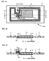
- Figs. 5A, 5B and 5c show an IC card 10B as a comparative example in a top view (5A) and cross-sectional views (5B) and (5C).
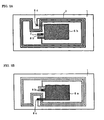
- Figs. 6A and 6B show a top view (6A) and a bottom view (6B) of the IC card 10B prior to mounting of the IC chip 3.
- the IC card 10B is provided with an antenna coil 2 and an IC chip 3 on one side of a transparent mica film 1. Electrodes 6a, 6b are formed on both sides of the mica film 1, and a mica capacitor 5 is constituted from these electrodes 6a, 6b and the mica film 1, which is sandwiched between the electrodes 6a, 6b.
- the dotted portion that appears in the mica capacitor 5 in Fig. 5A indicates the electrode 6a, which is formed on the bottom surface of the mica film 1.
- the antenna coil 2 in the IC card 10B can be printed on the mica film 1 in a coil pattern using a silver or other conductive paste, or can be formed by etching the conductive layer of a laminated sheet comprising a copper or other conductive layer formed on the surface of the mica film 1.
- the IC chip 3 is mounted in a facedown fashion on the mica film 1 using an anisotropically conductive adhesive 4.
- the IC chip 3 is mounted in such a manner that it steps over the antenna coil 2 between the IC chip terminals 3a and 3b, resulting in one terminal 3a contacting an inner terminal 2a of the antenna coil 2, and the other terminal 3b contacting an outer terminal 2b of the antenna coil 2.
- the mica capacitor 5 is constituted from the mica film 1 and the electrodes 6a and 6b formed on both sides thereof.
- the capacitor terminal 5a is formed on the electrode 6a, which has been formed on the bottom side of the mica film 1, and the capacitor terminal 5a is connected to the inner terminal 2aa of the antenna coil 2 via a through-hole 8a.
- the capacitor terminal 5b is formed on the electrode 6b of the mica capacitor 5, which has been formed on the top side of the mica film 1, and the capacitor terminal 5b is connected to wiring 7, which has been formed on the bottom side of the mica film 1, via a through-hole 8b.
- the wiring 7 is connected to an outer terminal 2bb of the antenna coil 2 via a through-hole 8c.
- the IC card 10B as shown in Figs. 5A to 5C can be manufactured, for example, as described below.
- Fig. 6A holes are formed for the through-holes 8a, 8b, 8c in the mica film 1, after which the electrode 6b on the top side of the mica capacitor 5 and the antenna coil 2 are printed on one side of the mica film 1, using a silver or other conductive paste.
- Fig. 6B the electrode 6a on the bottom side of the mica capacitor 5 and the wiring 7 are printed on the other side of the mica film 1.
- Printing the conductive paste fills the through-holes 8a, 8b, 8c with the conductive paste, causes passage through the through-holes 8a, 8b, 8c, and completes the connection between the antenna coil 2 and the mica capacitor 5.
- the IC chip 3 is mounted in facedown fashion on the topside of the mica film 1 using an anisotropically conductive adhesive 4.
- Any conventionally known adhesive may be used as this anisotropically conductive adhesive 4, and it may come in the form of a film, paste or any other form.
- a mica film 1 as a dielectric of the capacitor 5 in the IC card 10B prevents any deviation from occurring in the resonance frequency owing to absorbed moisture and improves the antenna characteristics. Furthermore, the fact that the mica film 1 serves as the mounting substrate of the antenna coil 2 and the IC chip 3 allows the selected IC chip to have a thinner profile than conventional IC chips where the mounting substrate is an entity separate from the dielectric of the capacitor 5. Moreover, by using the conductive paste, it is possible to form at the same time both the electrodes 6a, 6b of the capacitor 5 and the antenna coil 2 as well as the wiring 7 and through-holes 8a, 8b, 8c which are necessary for these to be connected, thereby making unnecessary any process for connecting them. This allows the manufacturing process to be streamlined and the IC chips to be produced at low cost.
- Figs. 1A to 1C depict an IC card 10A pertaining to an embodiment of the present invention in a top view (1A) and in cross-sectional views ((1B) and (1C)).
- the dotted portion in the mica capacitor 5 in Fig. 1A refers to the electrode 6a, which has been formed on the bottom side of the mica film 1.
- Figs. 2A and 2B show a top view (2A) and a bottom view (2B) of the IC card 10A prior to mounting of the IC chip 3.
- This IC card 10A is manufactured in essentially the same way as the aforementioned IC card 10B, while the capacitor terminal 5c, which is connected to the terminal 3b of the IC chip 3 via the wiring 7 and the through-hole 8b, is furnished from the electrode 6a on the bottom side of the mica film 1, in addition to the capacitor terminal 5b which is connected to the outer terminal 2b of the antenna coil 2 via the through-hole 8c.
- a capacitor terminal 5a which is connected to the other terminal 3a of the IC chip 3, is formed from the electrode 6b on the top side of the mica film 1, and this capacitor terminal 5a is linked to the inner terminal 2a of the antenna coil 2.
- this IC card 10A when the two terminals 3a and 3b of the IC chip 3 are respectively connected to the inner terminal 2a and the outer terminal 2b of the antenna coil 2, the IC chip 3 does not step over the antenna coil 2 between the two terminals 3a and 3b. It is also unnecessary for the total winding width of the antenna coil 2 to be kept between the two terminals 3a and 3b of the IC chip 3. According to this IC card 10A, therefore, considerable latitude is provided for the design of the antenna coil 2.
- IC card pertaining to the present invention can be sealed with a resin as necessary, or any desired sheet material can be laminated onto either the top or bottom side of the IC card.
- Fig. 3 shows an IC card in which the IC card 10A shown in Figs. 1A to 1C is sealed with a sealing resin 11 comprising an epoxy or other thermosetting resin, or a polyester or other hot melt resin, one side thereof being laminated with a outer layer film 13 of polyester or the like via an acrylic resin or other adhesive 12 and the other side of same being laminated with a release paper 15 via an adhesive 14, thereby constituting a label with identification function 10X which can be affixed to video films or other various articles.
- a sealing resin 11 comprising an epoxy or other thermosetting resin, or a polyester or other hot melt resin, one side thereof being laminated with a outer layer film 13 of polyester or the like via an acrylic resin or other adhesive 12 and the other side of same being laminated with a release paper 15 via an adhesive 14, thereby constituting a label with identification function 10
- the release paper 15 is peeled away, leaving a surface with the adhesive 14 affixed to the article and on the other hand a label surface having an outer layer film 13 which can be written on.
- a method for manufacturing a label 10X which uses such an IC card 10A can be seen in Fig. 4 , where an outer film 13 is affixed to one side of the IC card 10A via an adhesive (not shown), a sealing resin is applied to the opposite side, and an adhesive-backed release paper 15 is applied thereon using a roller 16, as heat and pressure are applied.
- the space between the outer layer film 13 and the release paper 15 can be adjusted to a specific width d.
- the label 10X shown in Fig. 3 can be thereby obtained.
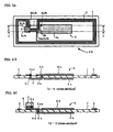
- Figs. 7A to 7C depict an IC card 10C pertaining to a further embodiment of the present invention configured as a label 10Y in a top view (7A) and in cross-sectional views ((7B) and (7C)).
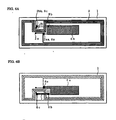
- Figs. 8A and 8B show a top view (8A) and bottom view (8B) of the IC card 10C prior to mounting of the IC chip 3.
- this IC card 10C has an antenna coil 2 which is circularly wound, as opposed to the antenna coil 2 of the aforementioned IC card 10A, which is rectangularly wound, it has virtually the same constitution as the IC card 10A.
- the capacitor terminal 5c which is connected to the terminal 3b on the IC chip 3 via the wiring 7 and the through-hole 8b, is furnished from the electrode 6a on the bottom side of the mica film 1, in addition to the capacitor terminal 5b which is connected to the outer terminal 2b of the antenna coil 2 via the through-hole 8c.
- the capacitor terminal 5a which is connected to the other terminal 3a of the IC chip 3 is formed from the electrode 6b on the top side of the mica film 1, and this capacitor terminal 5a is linked to the inner terminal 2a of the antenna coil 2. Therefore, in this IC card 10C, it is not necessary for the IC chip 3 to step over the antenna coil 2 between the two terminals 3a and 3b. It is also unnecessary for the total winding width of the antenna coil 2 to be kept between the two terminals 3a and 3b of the IC chip 3. Therefore, considerable latitude is provided for the design of the antenna coil 2.
- a land 9 on which the terminal of the IC chip 3 lies is formed on the mica film 1 of this IC card 10C.
- This land 9 does not directly connect to the antenna coil 2 or the capacitor 5, but it can be utilized as an earth or other wiring terminal. Moreover, it can act as a strut for ensuring that the IC chip 3 does not unnecessarily tilt when the IC chip is mounted.
- the IC card pertaining to the present invention is not limited to the aforementioned embodiments; it can assume various embodiments.
- the scope of the invention is defined by the appended claims.
- a mica capacitor is used, enabling the resonance frequency to be stabilized, and moreover, a mica film, which serves as a dielectric of the mica capacitor, is used as a substrate on which the antenna coil and IC chip are mounted, enabling the IC card profile to be reduced and the costs of manufacture lowered.
Landscapes
- Engineering & Computer Science (AREA)
- Physics & Mathematics (AREA)
- General Physics & Mathematics (AREA)
- Theoretical Computer Science (AREA)
- Computer Networks & Wireless Communication (AREA)
- Computer Hardware Design (AREA)
- Microelectronics & Electronic Packaging (AREA)
- Credit Cards Or The Like (AREA)
- Fixed Capacitors And Capacitor Manufacturing Machines (AREA)
Claims (3)
- Carte à circuit intégré, comprenant
un condensateur (5) avec un film (1) et des électrodes (6a, 6b) formées sur les deux faces du film (1) ;
une bobine (2) d'antenne ; et
un microcircuit intégré (3), où ledit film agit comme un substrat sur lequel ladite bobine (2) d'antenne et ledit microcircuit intégré (3) sont prévus, dans laquelle le microcircuit intégré (3) n'empiète pas sur la bobine (2) d'antenne,
caractérisée en ce que
le condensateur (5) est un condensateur au mica et le film (1) est un film au mica, dans laquelle l'une (6b) des électrodes du condensateur est prévue à l'intérieur de ladite bobine d'antenne et une première borne (5a) du condensateur est connectée à une première borne (3a) dudit microcircuit intégré (3) et est liée à une première borne (2a) de ladite bobine (2) d'antenne, une deuxième borne (5c) du condensateur est connectée à une deuxième borne (3b) dudit microcircuit intégré (3), et une troisième borne (5b) du condensateur est connectée à une deuxième borne (2b) de ladite bobine (2) d'antenne; et
ledit microcircuit intégré (3) est monté sur ledit film au mica à l'intérieur de ladite bobine (2) d'antenne. - Carte à circuit intégré selon la revendication 1, dans laquelle ladite carte à circuit intégré est scellée avec une résine (11), ladite carte à circuit intégré scellée a une première face et une deuxième face, ladite première face est stratifiée avec un film (13) de couche externe, et ladite deuxième face est stratifiée avec un papier (15) intercalaire.
- Procédé de fabrication de la carte à circuit intégré selon la revendication 1, comprenant le fait de former simultanément la bobine (2) d'antenne et une électrode du condensateur au mica en imprimant une pâte conductrice sur le film au mica.
Applications Claiming Priority (2)
| Application Number | Priority Date | Filing Date | Title |
|---|---|---|---|
| JP21495499 | 1999-07-29 | ||
| JP21495499A JP2001043336A (ja) | 1999-07-29 | 1999-07-29 | Icカード |
Publications (3)
| Publication Number | Publication Date |
|---|---|
| EP1073009A2 EP1073009A2 (fr) | 2001-01-31 |
| EP1073009A3 EP1073009A3 (fr) | 2001-06-13 |
| EP1073009B1 true EP1073009B1 (fr) | 2011-04-20 |
Family
ID=16664325
Family Applications (1)
| Application Number | Title | Priority Date | Filing Date |
|---|---|---|---|
| EP00116306A Expired - Lifetime EP1073009B1 (fr) | 1999-07-29 | 2000-07-27 | Carte à puce |
Country Status (7)
| Country | Link |
|---|---|
| US (1) | US6879258B2 (fr) |
| EP (1) | EP1073009B1 (fr) |
| JP (1) | JP2001043336A (fr) |
| KR (1) | KR20010030032A (fr) |
| CN (2) | CN1282940A (fr) |
| DE (1) | DE60045859D1 (fr) |
| TW (1) | TW480447B (fr) |
Families Citing this family (29)
| Publication number | Priority date | Publication date | Assignee | Title |
|---|---|---|---|---|
| KR100381780B1 (ko) * | 2000-11-10 | 2003-05-01 | 삼성에스디에스 주식회사 | Ic카드용 ic 모듈과 이를 사용하는 ic카드 |
| JP2002297040A (ja) * | 2001-03-30 | 2002-10-09 | Kawanishi Co Ltd | Icチップ付箋 |
| WO2005013360A1 (fr) * | 2003-08-05 | 2005-02-10 | Lintec Corporation | Substrat de montage de puce a bosse |
| WO2005071608A1 (fr) * | 2004-01-23 | 2005-08-04 | Semiconductor Energy Laboratory Co., Ltd. | Vignette, carte et etiquette d'identification |
| DE202004003701U1 (de) * | 2004-03-12 | 2004-08-12 | Cubit Electronics Gmbh | Flacher Transponder |
| KR101233421B1 (ko) * | 2004-09-09 | 2013-02-13 | 가부시키가이샤 한도오따이 에네루기 켄큐쇼 | 반도체 장치 |
| CN100508182C (zh) * | 2004-09-21 | 2009-07-01 | 日月光半导体制造股份有限公司 | 具有微带天线结构的半导体封装构造 |
| JP2007183919A (ja) * | 2005-12-05 | 2007-07-19 | Nec Corp | Rfidタグ |
| JP4235686B2 (ja) | 2006-03-30 | 2009-03-11 | 王子製紙株式会社 | Icモジュール、icインレット及びic実装体 |
| DE102006030819A1 (de) * | 2006-06-30 | 2008-01-03 | Smartrac Technology Ltd. | Chipkarte und Verfahren zur Herstellung einer Chipkarte |
| US8009101B2 (en) * | 2007-04-06 | 2011-08-30 | Murata Manufacturing Co., Ltd. | Wireless IC device |
| HK1109708A2 (zh) * | 2007-04-24 | 2008-06-13 | On Track Innovations Ltd. | 介面卡及仪器以及其形成工艺 |
| EP2180432B1 (fr) * | 2007-08-13 | 2016-09-14 | Fujitsu Limited | Etiquette radio et son procédé de fabrication |
| KR20120102173A (ko) * | 2007-09-13 | 2012-09-17 | 퀄컴 인코포레이티드 | 무선 전력 인가를 위한 안테나 |
| WO2010001469A1 (fr) * | 2008-07-02 | 2010-01-07 | 三菱電機株式会社 | Dispositif de communication sans fil |
| KR101075753B1 (ko) * | 2008-12-22 | 2011-10-24 | 삼성전자주식회사 | 안테나 장치 및 그 제조방법 |
| WO2010073627A1 (fr) * | 2008-12-22 | 2010-07-01 | 株式会社フジクラ | Antenne en couche mince et procede de fabrication associe |
| KR20120043021A (ko) * | 2009-07-28 | 2012-05-03 | 소니 케미카루 앤드 인포메이션 디바이스 가부시키가이샤 | 안테나 장치 및 통신 장치 |
| KR101620350B1 (ko) * | 2010-03-29 | 2016-05-13 | 삼성전자주식회사 | 이중 범프 구조를 갖는 반도체 칩 및 이를 포함하는 스마트 카드 |
| WO2011158844A1 (fr) * | 2010-06-18 | 2011-12-22 | 株式会社村田製作所 | Appareil terminal de communication et dispositif d'antenne |
| US9203548B2 (en) * | 2012-11-27 | 2015-12-01 | Diebold Self-Service Systems Division Of Diebold, Incorporated | Automated banking machine that outputs interference signals to jam reading ability of unauthorized card reader devices |
| FR3013152A1 (fr) * | 2013-11-14 | 2015-05-15 | Smart Packaging Solutions | Antenne double face pour carte a puce |
| FR3038105B1 (fr) | 2015-06-29 | 2017-08-04 | Oberthur Technologies | Module equipe d'un condensateur et d'une antenne, avec disposition d'electrode de condensateur amelioree |
| DE102016107982A1 (de) * | 2016-04-29 | 2017-11-02 | Infineon Technologies Ag | Chipkartenmodul, Chipkarte und Verfahren zum Bilden eines Chipkartenmoduls |
| KR102483645B1 (ko) * | 2017-03-06 | 2023-01-03 | 삼성전자주식회사 | 무선 통신 및 무선 전력 전송을 수행하는 통신 장치 및 대상으로부터 전기 신호를 송수신하는 전극 장치 |
| US10523258B2 (en) * | 2017-03-06 | 2019-12-31 | Samsung Electronics Co., Ltd. | Communication device to perform wireless communication and wireless power transfer, and electrode device to transmit and receive electrical signal from target |
| FR3073307B1 (fr) * | 2017-11-08 | 2021-05-28 | Oberthur Technologies | Dispositif de securite tel qu'une carte a puce |
| CN116745775A (zh) * | 2021-02-17 | 2023-09-12 | 富士通先端科技株式会社 | Rfid标签 |
| FR3131412B1 (fr) * | 2021-12-24 | 2024-01-05 | Wisekey Semiconductors | Module sans contact ayant une bobine d'antenne configurable |
Family Cites Families (23)
| Publication number | Priority date | Publication date | Assignee | Title |
|---|---|---|---|---|
| JPS60194625A (ja) * | 1984-03-16 | 1985-10-03 | Y D K:Kk | 双方向通信における分波装置 |
| JPS61188871U (fr) * | 1985-05-16 | 1986-11-25 | ||
| JPS6414095A (en) * | 1987-07-07 | 1989-01-18 | Mitsubishi Electric Corp | Ic card |
| JP2758030B2 (ja) * | 1988-07-04 | 1998-05-25 | ソニー株式会社 | 薄型電子機器とその製造方法 |
| JPH0414282A (ja) * | 1990-05-08 | 1992-01-20 | Mitsubishi Gas Chem Co Inc | 高周波回路用基板 |
| DE69230171T2 (de) * | 1991-04-03 | 2000-04-13 | Integrated Silicon Design Pty. Ltd., Adelaide | Warensortiersystem |
| JP2993186B2 (ja) * | 1991-06-28 | 1999-12-20 | 株式会社デンソー | 航空機手荷物管理システム |
| WO1993002479A1 (fr) * | 1991-07-16 | 1993-02-04 | Asahi Kasei Kogyo Kabushiki Kaisha | Capteur a semiconductor et son procede de fabrication |
| JP2715819B2 (ja) * | 1992-07-06 | 1998-02-18 | トヨタ自動車株式会社 | 自動変速機の変速制御装置 |
| US5442334A (en) * | 1992-07-20 | 1995-08-15 | Stoplift Corporation | Security system having deactivatable security tag |
| DE4416697A1 (de) * | 1994-05-11 | 1995-11-16 | Giesecke & Devrient Gmbh | Datenträger mit integriertem Schaltkreis |
| US5852289A (en) * | 1994-09-22 | 1998-12-22 | Rohm Co., Ltd. | Non-contact type IC card and method of producing the same |
| EP0704928A3 (fr) * | 1994-09-30 | 1998-08-05 | HID Corporation | Système transpondeur radiofréquence avec interrogation à résonance parallèle et réponse à résonance en série |
| JP2814477B2 (ja) * | 1995-04-13 | 1998-10-22 | ソニーケミカル株式会社 | 非接触式icカード及びその製造方法 |
| DE19529640A1 (de) * | 1995-08-11 | 1997-02-13 | Giesecke & Devrient Gmbh | Spulenelement für einen Datenträger mit integriertem Schaltkreis und nichtberührender Kopplung |
| EP0868706A1 (fr) * | 1995-12-22 | 1998-10-07 | Sempac SA | Procede de production d'une carte a puces pour utilisations sans contact |
| JPH1013312A (ja) * | 1996-06-20 | 1998-01-16 | Sony Corp | データ処理装置および方法、並びに、送受信装置および方法 |
| US5708419A (en) * | 1996-07-22 | 1998-01-13 | Checkpoint Systems, Inc. | Method of wire bonding an integrated circuit to an ultraflexible substrate |
| JPH10203060A (ja) * | 1997-01-20 | 1998-08-04 | Toshiba Corp | 無線カード |
| US5883582A (en) * | 1997-02-07 | 1999-03-16 | Checkpoint Systems, Inc. | Anticollision protocol for reading multiple RFID tags |
| JPH111607A (ja) * | 1997-04-18 | 1999-01-06 | Toray Ind Inc | 熱可塑性樹脂組成物およびそれからなるシートまたはカード |
| EP0886232B1 (fr) * | 1997-06-20 | 2007-09-05 | Hitachi, Ltd. | Lecteur-enregistreur, système d'alimentation et système de communication |
| US6043746A (en) * | 1999-02-17 | 2000-03-28 | Microchip Technology Incorporated | Radio frequency identification (RFID) security tag for merchandise and method therefor |
-
1999
- 1999-07-29 JP JP21495499A patent/JP2001043336A/ja active Pending
-
2000
- 2000-07-14 TW TW089114080A patent/TW480447B/zh not_active IP Right Cessation
- 2000-07-27 EP EP00116306A patent/EP1073009B1/fr not_active Expired - Lifetime
- 2000-07-27 DE DE60045859T patent/DE60045859D1/de not_active Expired - Lifetime
- 2000-07-28 KR KR1020000043754A patent/KR20010030032A/ko not_active Ceased
- 2000-07-28 CN CN00122243A patent/CN1282940A/zh active Pending
- 2000-07-28 CN CN2006100845889A patent/CN1877609B/zh not_active Expired - Lifetime
-
2003
- 2003-12-17 US US10/736,603 patent/US6879258B2/en not_active Expired - Lifetime
Also Published As
| Publication number | Publication date |
|---|---|
| US20040124983A1 (en) | 2004-07-01 |
| TW480447B (en) | 2002-03-21 |
| US6879258B2 (en) | 2005-04-12 |
| CN1282940A (zh) | 2001-02-07 |
| JP2001043336A (ja) | 2001-02-16 |
| EP1073009A3 (fr) | 2001-06-13 |
| CN1877609A (zh) | 2006-12-13 |
| EP1073009A2 (fr) | 2001-01-31 |
| KR20010030032A (ko) | 2001-04-16 |
| DE60045859D1 (de) | 2011-06-01 |
| CN1877609B (zh) | 2010-05-12 |
Similar Documents
| Publication | Publication Date | Title |
|---|---|---|
| US6879258B2 (en) | IC card having a mica film for stable resonance frequency and enhanced antenna properties | |
| KR100770193B1 (ko) | Ic 카드 | |
| US7078304B2 (en) | Method for producing an electrical circuit | |
| JP4052111B2 (ja) | 無線情報記憶媒体 | |
| JP2005129019A (ja) | Icカード | |
| JP4641096B2 (ja) | 非接触式データキャリア装置とブースターアンテナ部用配線部材 | |
| US7967216B2 (en) | Wireless IC device | |
| KR100799140B1 (ko) | Rfid 태그 및 그 제조 방법 | |
| KR100833752B1 (ko) | 박형 집적회로 태그 및 그 제조 방법 | |
| US9627759B2 (en) | Antenna device antenna module | |
| AU2003243162A2 (en) | Method for producing an electrical circuit | |
| US10476147B2 (en) | Antenna device and method of manufacturing the same | |
| CN108369658A (zh) | 具有包括电气和/或电子模块的可调节的lc电路的射频装置 | |
| WO2007034764A1 (fr) | Support de stockage d’informations sans contact et son procédé de fabrication | |
| CN108370087B (zh) | 具有cms器件的单面天线模块 | |
| JP4562892B2 (ja) | 非接触式データキャリア装置とブースターアンテナ部用配線部材 | |
| JP2012094948A (ja) | 非接触通信記録媒体用インレット及びその製造方法及び非接触通信記録媒体 | |
| JP4641095B2 (ja) | 非接触式データキャリア装置とブースターアンテナ部用配線部材 | |
| JP2002207982A (ja) | 接触非接触両用icモジュール及びicカード | |
| KR100503048B1 (ko) | 비접촉형 아이 씨 카드 제조방법 | |
| KR20050111174A (ko) | Rfid 태그 및 그 제조방법 | |
| KR20060132299A (ko) | 무선주파수 특성의 튜닝 방법 및 이를 사용하는 rfid태그 |
Legal Events
| Date | Code | Title | Description |
|---|---|---|---|
| PUAI | Public reference made under article 153(3) epc to a published international application that has entered the european phase |
Free format text: ORIGINAL CODE: 0009012 |
|
| AK | Designated contracting states |
Kind code of ref document: A2 Designated state(s): DE FR GB NL |
|
| AX | Request for extension of the european patent |
Free format text: AL;LT;LV;MK;RO;SI |
|
| PUAL | Search report despatched |
Free format text: ORIGINAL CODE: 0009013 |
|
| AK | Designated contracting states |
Kind code of ref document: A3 Designated state(s): AT BE CH CY DE DK ES FI FR GB GR IE IT LI LU MC NL PT SE |
|
| AX | Request for extension of the european patent |
Free format text: AL;LT;LV;MK;RO;SI |
|
| 17P | Request for examination filed |
Effective date: 20011113 |
|
| AKX | Designation fees paid |
Free format text: DE FR GB NL |
|
| RAP1 | Party data changed (applicant data changed or rights of an application transferred) |
Owner name: SONY CHEMICAL & INFORMATION DEVICE CORPORATION |
|
| 17Q | First examination report despatched |
Effective date: 20061211 |
|
| 17Q | First examination report despatched |
Effective date: 20061211 |
|
| GRAP | Despatch of communication of intention to grant a patent |
Free format text: ORIGINAL CODE: EPIDOSNIGR1 |
|
| GRAS | Grant fee paid |
Free format text: ORIGINAL CODE: EPIDOSNIGR3 |
|
| GRAA | (expected) grant |
Free format text: ORIGINAL CODE: 0009210 |
|
| AK | Designated contracting states |
Kind code of ref document: B1 Designated state(s): DE FR GB NL |
|
| REG | Reference to a national code |
Ref country code: GB Ref legal event code: FG4D |
|
| REF | Corresponds to: |
Ref document number: 60045859 Country of ref document: DE Date of ref document: 20110601 Kind code of ref document: P |
|
| REG | Reference to a national code |
Ref country code: DE Ref legal event code: R096 Ref document number: 60045859 Country of ref document: DE Effective date: 20110601 |
|
| REG | Reference to a national code |
Ref country code: NL Ref legal event code: T3 |
|
| PGFP | Annual fee paid to national office [announced via postgrant information from national office to epo] |
Ref country code: FR Payment date: 20110729 Year of fee payment: 12 |
|
| PGFP | Annual fee paid to national office [announced via postgrant information from national office to epo] |
Ref country code: GB Payment date: 20110721 Year of fee payment: 12 |
|
| PGFP | Annual fee paid to national office [announced via postgrant information from national office to epo] |
Ref country code: NL Payment date: 20110725 Year of fee payment: 12 |
|
| PLBE | No opposition filed within time limit |
Free format text: ORIGINAL CODE: 0009261 |
|
| STAA | Information on the status of an ep patent application or granted ep patent |
Free format text: STATUS: NO OPPOSITION FILED WITHIN TIME LIMIT |
|
| 26N | No opposition filed |
Effective date: 20120123 |
|
| REG | Reference to a national code |
Ref country code: DE Ref legal event code: R097 Ref document number: 60045859 Country of ref document: DE Effective date: 20120123 |
|
| PGFP | Annual fee paid to national office [announced via postgrant information from national office to epo] |
Ref country code: DE Payment date: 20121031 Year of fee payment: 13 |
|
| REG | Reference to a national code |
Ref country code: NL Ref legal event code: V1 Effective date: 20130201 |
|
| GBPC | Gb: european patent ceased through non-payment of renewal fee |
Effective date: 20120727 |
|
| REG | Reference to a national code |
Ref country code: FR Ref legal event code: ST Effective date: 20130329 |
|
| PG25 | Lapsed in a contracting state [announced via postgrant information from national office to epo] |
Ref country code: NL Free format text: LAPSE BECAUSE OF NON-PAYMENT OF DUE FEES Effective date: 20130201 Ref country code: GB Free format text: LAPSE BECAUSE OF NON-PAYMENT OF DUE FEES Effective date: 20120727 Ref country code: FR Free format text: LAPSE BECAUSE OF NON-PAYMENT OF DUE FEES Effective date: 20120731 |
|
| REG | Reference to a national code |
Ref country code: DE Ref legal event code: R119 Ref document number: 60045859 Country of ref document: DE Effective date: 20140201 |
|
| PG25 | Lapsed in a contracting state [announced via postgrant information from national office to epo] |
Ref country code: DE Free format text: LAPSE BECAUSE OF NON-PAYMENT OF DUE FEES Effective date: 20140201 |