EP1011149A2 - Halbleiter-Speicheranordnung und Verfahren zur Herstellung - Google Patents
Halbleiter-Speicheranordnung und Verfahren zur Herstellung Download PDFInfo
- Publication number
- EP1011149A2 EP1011149A2 EP99124901A EP99124901A EP1011149A2 EP 1011149 A2 EP1011149 A2 EP 1011149A2 EP 99124901 A EP99124901 A EP 99124901A EP 99124901 A EP99124901 A EP 99124901A EP 1011149 A2 EP1011149 A2 EP 1011149A2
- Authority
- EP
- European Patent Office
- Prior art keywords
- group
- element selected
- memory device
- semiconductor memory
- ferroelectric material
- Prior art date
- Legal status (The legal status is an assumption and is not a legal conclusion. Google has not performed a legal analysis and makes no representation as to the accuracy of the status listed.)
- Withdrawn
Links
Images






Classifications
-
- H—ELECTRICITY
- H10—SEMICONDUCTOR DEVICES; ELECTRIC SOLID-STATE DEVICES NOT OTHERWISE PROVIDED FOR
- H10D—INORGANIC ELECTRIC SEMICONDUCTOR DEVICES
- H10D30/00—Field-effect transistors [FET]
- H10D30/60—Insulated-gate field-effect transistors [IGFET]
- H10D30/701—IGFETs having ferroelectric gate insulators, e.g. ferroelectric FETs
-
- H—ELECTRICITY
- H10—SEMICONDUCTOR DEVICES; ELECTRIC SOLID-STATE DEVICES NOT OTHERWISE PROVIDED FOR
- H10D—INORGANIC ELECTRIC SEMICONDUCTOR DEVICES
- H10D64/00—Electrodes of devices having potential barriers
- H10D64/01—Manufacture or treatment
- H10D64/031—Manufacture or treatment of data-storage electrodes
- H10D64/033—Manufacture or treatment of data-storage electrodes comprising ferroelectric layers
Definitions
- the present invention relates to a semiconductor memory device including a film formed of a ferroelectric material and a method for producing the same, and specifically to a non-volatile memory device including a film formed of a ferroelectric material and a method for producing the same.
- Non-volatile memory devices including a film-formed of a ferroelectric material are roughly classified into two types. One type is referred to as a capacitor type device, and the other is referred to as an MFS (metal-ferroelectric-semiconductor) FET device.
- MFS metal-ferroelectric-semiconductor
- a capacitor type device has a capacitor structure including a ferroelectric thin film interposed between two electrodes. Information is read or written by detecting whether or not there is an inverted current which flows when the spontaneous polarization of the ferroelectric film is inverted.
- the capacitor type device mainly has the following two problems: (1) since the stored information is destroyed when the information is read, rewrite of the information is required; and (2) each time the information is read, the spontaneous polarization is inverted, which causes fatigue.
- the capacitor type device also has an advantage in that the ferroelectric film, which is provided on a Pt electrode or the like, tends to have relatively high quality. Due to this advantage, the capacitor type device has been developed for practical use.
- oxide ferroelectric materials having a relatively high value of spontaneous polarization are the main targets of study.
- oxide ferroelectric materials are, for example, PZT (lead zirconate titanate) represented by Pb(Zr x Ti 1-x )O 3 (O ⁇ x ⁇ 1), and Bi-based layered oxides including BrBi 2 Ta 2 O 9 and Bi 4 Ti 3 O 12 .
- An MFSFET device allows non-destructive information read.
- An MFSFET device includes an Si (silicon) substrate having, in a surface area thereof, a source region and a drain region each formed of an impurity diffusive region and a channel region sandwiched between the source region and the drain region; a gate insulating layer formed of a ferroelectric thin film provided on the channel region; and a gate electrode provided on the ferroelectric thin film.
- the ferroelectric thin film is included in place of a gate oxide film included in a usual MOS (metal-oxide-semiconductor)FET.
- MOS metal-oxide-semiconductor
- Information is written into the MFSFET device by applying a positive or negative voltage between the gate electrode and the Si substrate to fix the polarization direction of the ferroelectric thin film.
- Information is read from the MFSFET device in a non-destructive manner by detecting the conductivity state of the channel region. The conductivity state of the channel region changes in accordance with the direction of the polarization direction of the ferroelectric thin film.
- the ferroelectric thin film is required to have a polarization charge amount which is only sufficient to change the potential on the surface of the Si substrate.
- the value of the spontaneous polarization required for the MFSFET device is smaller than that required for the capacitor type device.
- the MFSFET device realizes non-destructive information read and accordingly does not require rewrite of the information as is required in the capacitor type device.
- the MFSFET device does not have the problem of the fatigue by the polarization which is unavoidable in the case of the capacitor type device.
- the MFSFET device also needs only a smaller memory cell area than the capacitor type device, and thus is highly suitable for higher integration.
- the MFSFET device has the following problems in terms of stability.
- Formation of a ferroelectric thin film of an oxide ferroelectric material of, for example, PZT, SrBi 2 Ta 2 O 9 or Bi 4 Ti 3 O 12 directly on the Si substrate usually includes a process of heat treatment performed at a temperature as high as 500°C to 800°C. Accordingly, an element of the ferroelectric material, e.g., Pb or Bi, is diffused in the Si substrate to form an interface reaction layer; or an Si oxide film is formed at a surface of the Si substrate by oxygen. This undesirably results in, for example, deterioration in the crystallinity of the ferroelectric thin film or an increase in the interface state density (problem 1).
- the oxide ferroelectric material is easily reduced by hydrogen gas sintering, etching using hydrogen (H), or metal or insulating film formation which are included in a usual Si-MOSFET process. As a result, the ferroelectric material is changed from an insulating material into a conductive material and thus changes the characteristics thereof. As appreciated from this, the oxide ferroelectric material is not properly usable in the usual Si-MOSFET process (problem 3).
- Fluorine (F) which is an element of a fluoride, has problems in terms of stability that fluorine is easily diffused in the Si substrate to form an Si-F bond, thus increasing an interface level (problem 4); and that fluorine reacts with water (problem 5).
- a semiconductor memory device includes a semiconductor substrate having a channel therein; a gate insulating layer formed of a ferroelectric material provided on the semiconductor substrate; and a gate electrode provided on the gate insulating layer.
- the ferroelectric material includes a nitrogen (N) and at least one element selected from the group consisting of Mg, Sr, Ba and Ca.
- the ferroelectric material is represented by formula (1): A 2 BN 3 where A is one element selected from the group consisting of Mg, Sr, Ba and Ca, and B is one element selected from the group consisting of V, Nb, Ta and Mn.
- the ferroelectric material is represented by formula (2): (A x B 1-x ) 2 CN 3 where x is in the range of 0 ⁇ x ⁇ 1, A and B are each one element selected from the group consisting of Mg, Sr, Ba and Ca, and C is one element selected from the group consisting of V, Nb, Ta and Mn.
- the ferroelectric material is represented by formula (3): (A x B 1-x ) 2 (C y D 1-y )N 3 where x is in the range of 0 ⁇ x ⁇ 1, y is in the range of 0 ⁇ y ⁇ 1, A and B are each one element selected from the group consisting of Mg, Sr, Ba and Ca, and C and D are each one element selected from the group consisting of V, Nb, Ta and Mn.
- the ferroelectric material is represented by formula (4): AB 2 N 4 where A is one element selected from the group consisting of Mg, Sr, Ba and Ca, and B is one element selected from the group consisting of V, Nb, Ta and Mn.
- the ferroelectric material is represented by formula (5): (A x B 1-x )C 2 N 4 where x is in the range of 0 ⁇ x ⁇ 1, A and B are each one element selected from the group consisting of Mg, Sr, Ba and Ca, and C is one element selected from the group consisting of V, Nb, Ta and Mn.
- the ferroelectric material is represented by formula (6): (A x B 1-x ) 2 (C y D 1-y ) 2 N 4 where x is in the range of 0 ⁇ x ⁇ 1, y is in the range of 0 ⁇ y ⁇ 1, A and B are each one element selected from the group consisting of Mg, Sr, Ba and Ca, and C and D are each one element selected from the group consisting of V, Nb, Ta and Mn.
- the ferroelectric material is represented by formula (7): A 2 BN 2 where A and B are each one element selected from the group consisting of Mg, Sr, Ba and Ca.
- the ferroelectric material is represented by formula (8): (A x B 1-x ) 2 (C y D 1-y )N 2 where x is in the range of 0 ⁇ x ⁇ 1, y is in the range of 0 ⁇ y ⁇ 1, A, B, C and D are each one element selected from the group consisting of Mg, Sr, Ba and Ca.
- the ferroelectric material is represented by formula (9): A 3 B 2 N 4 where A is one element selected from the group consisting of Mg, Sr, Ba and Ca, and B is one element selected from the group consisting of Al, Y, La, Sc, Co, Gd, Ce, Nd, Er, V, Ti, Ta, Nb and Mn.
- the ferroelectric material is represented by formula (10): (A x B 1-x ) 3 C 2 N 4 where x is in the range of 0 ⁇ x ⁇ 1, A and B are each one element selected from the group consisting of Mg, Sr, Ba and Ca, and C is one element selected from the group consisting of Al, Y, La, Sc, Co, Gd, Ce, Nd, Er, V, Ti, Ta, Nb and Mn.
- the ferroelectric material is represented by formula (11): (A x B 1-x ) 3 (C y D 1-y ) 2 N 4 where x is in the range of 0 ⁇ x ⁇ 1, y is in the range of 0 ⁇ y ⁇ 1, A and B are each one element selected from the group consisting of Mg, Sr, Ba and Ca, and C and D are each one element selected from the group consisting of Al, Y, La, Sc, Co, Gd, Ce, Nd, Er, V, Ti, Ta, Nb and Mn.
- the ferroelectric material is represented by formula (12): A 3 B 5 N 7 where A is one element selected from the group consisting of Mg, Sr, Ba and Ca, and B is one element selected from the group consisting of Al, Y, La, Sc, Co, Gd, Ce, Nd, Er, V, Ti, Ta, Nb and Mn.
- the ferroelectric material is represented by formula (13): (A x B 1-x ) 3 C 5 N 7 where x is in the range of 0 ⁇ x ⁇ 1, A and B are each one element selected from the group consisting of Mg, Sr, Ba and Ca, and C is one element selected from the group consisting of Al, Y, La, Sc, Co, Gd, Ce, Nd, Er, V, Ti, Ta, Nb and Mn.
- the ferroelectric material is represented by formula (14): (A x B 1-x ) 3 (C y D 1-y ) 5 N 7 where x is in the range of 0 ⁇ x ⁇ 1, y is in the range of 0 ⁇ y ⁇ 1, A and B are each one element selected from the group consisting of Mg, Sr, Ba and Ca, and C and D are each one element selected from the group consisting of Al, Y, La, Sc, Co, Gd, Ce, Nd, Er, V, Ti, Ta, Nb and Mn.
- the ferroelectric material is represented by formula (15): A 2 B 3 C 2 N 7 where A is one element selected from the group consisting of Mg, Sr, Ba and Ca, B is one element selected from the group consisting of Al, Y, La, Sc, Co, Gd, Ce, Nd, Er, V, Ti, Ta, Nb and Mn, and C is one element selected from the group consisting of Ti, Ta, Mn, Co, Zr, Hf, V and Nb.
- A is one element selected from the group consisting of Mg, Sr, Ba and Ca
- B is one element selected from the group consisting of Al, Y, La, Sc, Co, Gd, Ce, Nd, Er, V, Ti, Ta, Nb and Mn
- C is one element selected from the group consisting of Ti, Ta, Mn, Co, Zr, Hf, V and Nb.
- the ferroelectric material is represented by formula (16): (A x B 1-x ) 2 C 3 D 2 N 7 where x is in the range of 0 ⁇ x ⁇ 1, A and B are each one element selected from the group consisting of Mg, Sr, Ba and Ca, C is one element selected from the group consisting of Al, Y, La, Sc, Co, Gd, Ce, Nd, Er, V, Ti, Ta, Nb and Mn, and D is one element selected from the group consisting of Ti, Ta, Mn, Co, Zr, Hf, V and Nb.
- the ferroelectric material is represented by formula (17): (A x B 1-x ) 2 (C y D 1-y ) 3 (E z F 1-z ) 2 N 7 where x is in the range of 0 ⁇ x ⁇ 1, y is in the range of 0 ⁇ y ⁇ 1, z is in the range of 0 ⁇ z ⁇ 1,
- a and B are each one element selected from the group consisting of Mg, Sr, Ba and Ca
- C and D are each one element selected from the group consisting of Al, Y, La, Sc, Co, Gd, Ce, Nd, Er, V, Ti, Ta, Nb and Mn
- E and F are each one element selected from the group consisting of Ti, Ta, Mn, Co, Zr, Hf, V and Nb.
- the semiconductor memory device further includes a buffer layer between the semiconductor substrate and the gate insulating layer, wherein the buffer layer is formed of one of SiN and SiO 2 .
- a method for producing a semiconductor memory device includes the steps of forming a gate insulating layer formed of a ferroelectric material containing nitrogen and at least one element selected from the group consisting of Mg, Sr, Ba and Ca on a semiconductor substrate; and heat-treating the gate insulating layer formed on the semiconductor substrate in one of an ammonia atmosphere and a nitrogen radical ion-containing atmosphere.
- the ammonia atmosphere is an ammonia plasma atmosphere.
- a semiconductor memory device includes a semiconductor substrate having a channel therein; a gate insulating layer provided on the semiconductor substrate; a gate electrode provided on the gate insulating layer; a buffer layer formed of SiN provided between the semiconductor substrate and the gate insulating layer.
- the gate insulating layer is formed of a fluoride ferroelectric material.
- a method for producing a semiconductor memory device includes the steps of forming an SiO 2 layer on a semiconductor substrate; nitriding the SiO 2 layer in one of an ammonia atmosphere, an N 2 O atmosphere, and a nitrogen radical ion-containing atmosphere; forming a gate insulating layer formed of a fluoride ferroelectric material on the nitrided SiO 2 layer; and forming a gate electrode on the gate insulating layer.
- the ammonia atmosphere is an ammonia plasma atmosphere.
- a method for producing a semiconductor memory device includes the steps of forming a gate insulating layer formed of a fluoride ferroelectric material containing fluorine and at least one element selected from the group consisting of Mg, Sr, Ba and Ca on a semiconductor substrate; and nitriding the gate insulating layer formed on the semiconductor substrate in one of an ammonia atmosphere and a nitrogen radical ion-containing atmosphere.
- the ammonia atmosphere is an ammonia plasma atmosphere.
- the fluoride ferroelectric material is one material selected from the group consisting of BaMgF 4 , BaCoF 4 , BaNiF 4 and BaZnF 4 .
- the fluoride ferroelectric material is one material selected from the group consisting of BaMgF 4 , BaCoF 4 , BaNiF 4 and BaZnF 4 .
- the fluoride ferroelectric material is represented by formula (18): ABF 5 where A is one element selected from the group consisting of Mg, Sr, Ba and Ca, and B is one element selected from the group consisting of Al, Y, La, Sc, Co, Gd, Ce, Nd, Er, V, Ti, Ta, Nb and Mn.
- the fluoride ferroelectric material is represented by formula (18): ABF 5 where A is one element selected from the group consisting of Mg, Sr, Ba and Ca, and B is one element selected from the group consisting of Al, Y, La, Sc, Co, Gd, Ce, Nd, Er, V, Ti, Ta, Nb and Mn.
- the fluoride ferroelectric material is represented by formula (19): (A x B 1-x )(C y D 1-y )F 5 where x is in the range of 0 ⁇ x ⁇ 1, y is in the range of 0 ⁇ y ⁇ 1, A and B are each one element selected from the group consisting of Mg, Sr, Ba and Ca, and C and D are each one element selected from the group consisting of Al, Y, La, Sc, Co, Gd, Ce, Nd, Er, V, Ti, Ta, Nb and Mn.
- the fluoride ferroelectric material is represented by formula (19): (A x B 1-x )(C y D 1-y )F 5 where x is in the range of 0 ⁇ x ⁇ 1, y is in the range of 0 ⁇ y ⁇ 1, A and B are each one element selected from the group consisting of Mg, Sr, Ba and Ca, and C and D are each one element selected from the group consisting of Al, Y, La, Sc, Co, Gd, Ce, Nd, Er, V, Ti, Ta, Nb and Mn.
- the fluoride ferroelectric material is represented by formula (20): ABF 6 where A is one element selected from the group consisting of Mg, Sr, Ba and Ca, and B is one element selected from the group consisting of Ti, Ta, Mn, Co, Zr, Hf, V and Nb.
- the fluoride ferroelectric material is represented by formula (20): ABF 6 where A is one element selected from the group consisting of Mg, Sr, Ba and Ca, and B is one element selected from the group consisting of Ti, Ta, Mn, Co, Zr, Hf, V and Nb.
- the fluoride ferroelectric material is represented by formula (21): (A x B 1-x )(C y D 1-y )F 6 where x is in the range of 0 ⁇ x ⁇ 1, y is in the range of 0 ⁇ y ⁇ 1, A and B are each one element selected from the group consisting of Mg, Sr, Ba and Ca, and C and D are each one element selected from the group consisting of Ti, Ta, Mn, Co, Zr, Hf, V and Nb.
- the fluoride ferroelectric material is represented by formula (21): (A x B 1-x )(C y D 1-y )F 6 where x is in the range of 0 ⁇ x ⁇ 1, y is in the range of 0 ⁇ y ⁇ 1, A and B are each one element selected from the group consisting of Mg, Sr, Ba and Ca, and C and D are each one element selected from the group consisting of Ti, Ta, Mn, Co, Zr, Hf, V and Nb.
- the fluoride ferroelectric material is represented by formula (22): A 5 B 3 F 19 where A is one element selected from the group consisting of Mg, Sr, Ba and Ca, and B is one element selected from the group consisting of Al, Y, La, Sc, Co, Gd, Ce, Nd, Er, V, Ti, Ta, Nb and Mn.
- the fluoride ferroelectric material is represented by formula (22): A 5 B 3 F 19 where A is one element selected from the group consisting of Mg, Sr, Ba and Ca, and B is one element selected from the group consisting of Al, Y, La, Sc, Co, Gd, Ce, Nd, Er, V, Ti, Ta, Nb and Mn.
- the fluoride ferroelectric material is represented by formula (23): (A x B 1-x ) 5 (C y D 1-y ) 3 F 19 where x is in the range of 0 ⁇ x ⁇ 1, y is in the range of 0 ⁇ y ⁇ 1, A and B are each one element selected from the group consisting of Mg, Sr, Ba and Ca, and C and D are each one element selected from the group consisting of Al, Y, La, Sc, Co, Gd, Ce, Nd, Er, V, Ti, Ta, Nb and Mn.
- the fluoride ferroelectric material is represented by formula (23): (A x B 1-x ) 5 (C y D 1-y ) 3 F 19 where x is in the range of 0 ⁇ x ⁇ 1, y is in the range of 0 ⁇ y ⁇ 1, A and B are each one element selected from the group consisting of Mg, Sr, Ba and Ca, and C and D are each one element selected from the group consisting of Al, Y, La, Sc, Co, Gd, Ce, Nd, Er, V, Ti, Ta, Nb and Mn.
- a semiconductor memory device includes a semiconductor substrate having a channel therein; a buffer layer formed of at least one of MgSiO 3 , Mg 2 SiO 4 , SrSiO 3 , Sr 2 SiO 4 , (Mg x Sr 1-x )SiO 3 and (Mg x Sr 1-x ) 2 SiO 4 (where 0 ⁇ x ⁇ 1) provided on the semiconductor substrate; a gate insulating layer formed of a ferroelectric material provided on the buffer layer; and a gate electrode provided on the gate insulating layer.
- the ferroelectric material includes at least one element selected from the group consisting of Mg and Sr.
- the ferroelectric material is formed of at least one material selected from the group consisting of (Ba x Sr 1-x )MgF 4 and Ba(Mg x Sr 1-x )F 4 , where 0 ⁇ x ⁇ 1.
- a method for producing a semiconductor memory device includes the steps of forming a buffer layer formed of SiN on an Si substrate; forming an SrTiO 3 layer on the buffer layer formed of SiN by sputtering; forming a gate insulating layer formed of a ferroelectric material on the SrTiO 3 layer; and forming a gate electrode on the gate insulating layer.
- the buffer layer is formed by directly nitriding the Si substrate.
- a method for producing a semiconductor memory device includes the steps of forming a buffer layer formed of SiO 2 on an Si substrate; nitriding the buffer layer formed of SiO 2 using one of an ammonia atmosphere, an N 2 O gas atmosphere, and a nitrogen radical ion-containing atmosphere; forming an SrTiO 3 layer on the buffer layer formed of the nitrided SiO 2 by sputtering; forming a gate insulating layer formed of a ferroelectric material on the SrTiO3 layer; and forming a gate electrode on the gate insulating layer.
- a method for producing a semiconductor memory device includes the steps of forming a thin TiSr layer an Si substrate; forming an SrTiO 3 layer on the thin TiSr layer; forming a gate insulating layer formed of ferroelectric material on the SrTiO 3 layer: and forming a gate electrode on the gate insulating layer.
- the SrTiO 3 layer is formed by sputtering where the Si substrate has a temperature of about 300°C or less.
- the SrTiO 3 layer is formed on the thin TiSr layer by sputtering, and the step of forming the SrTiO 3 layer includes the steps of using an Ar gas, and using an Ar/O 2 gas.
- the method for producing a semiconductor memory device further includes the step of heat-treating the SrTiO 3 layer in one of an oxygen gas atmosphere and an ozone-containing oxygen gas atmosphere at a temperature of about 300°C or less.
- the ferroelectric layer acting as a gate insulating layer does not include Pb, Bi or other elements which are highly volatile, and includes a nitride excluding oxygen. Since formation of such a ferroelectric layer does not need heat treatment, formation of an interface reaction layer or a silicon oxide layer at an interface between the semiconductor substrate and the ferroelectric layer is suppressed. Therefore, the crystallinity in the ferroelectric layer is not deteriorated or the interface state density is not increased. Thus, satisfactory interface characteristics are obtained. The above-mentioned problem 1 is solved.
- the ferroelectric layer according to the present invention has a low specific dielectric constant. Therefore, the effective voltage applied on the ferroelectric portion of the film is not decreased. Accordingly, the operating voltage is not increased.
- the above-mentioned problem 2 is solved.
- the nitride ferroelectric layer according to the present invention is not likely to be reduced by hydrogen gas sintering, etching using hydrogen, or metal or insulating film formation which are included in a usual Si-MOSFET process. Thus, the device characteristics are maintained stable.
- the above-mentioned problem 3 is solved.
- the buffer layer between the semiconductor substrate and the fluoride ferroelectric layer is formed of SiN, or SiO 2 having a nitrided surface
- the buffer layer acts as a barrier against the diffusion of fluorine which is contained in the fluoride ferroelectric layer in a large amount during heat treatment processes of, for example, formation of the ferroelectric layer, and ion implantation and annealing for activation of the semiconductor substrate.
- an increase in the interface level caused by the diffusion of fluorine is prevented.
- An increase in the thickness of the SiO 2 layer caused by the diffusion of oxygen released from the Si-O bond is also prevented.
- the reliability of the MFSFET device is improved, solving the above-mentioned problem 4.
- the buffer layer has a relatively high dielectric constant.
- the crystallinity of the ferroelectric layer is improved and a satisfactory interface between the semiconductor substrate and the ferroelectric layer is realized.
- problem 6 is solved.
- the MgSiO 3 , Mg 2 SiO 4 , SrSiO 3 , Sr 2 SiO 4 , (Mg x Sr 1-x )SiO 3 and (Mg x Sr 1-x ) 2 SiO 4 include both (i) Mg or Sr included in the ferroelectric layer and (ii) SiO 2 , realizing a satisfactory interface characteristic with silicon.
- the SrTiO 3 layer is formed by sputtering after the buffer layer formed of SiN, or SiO 2 having a nitrided surface obtained by an ammonia gas, an N 2 O gas or a nitrogen radical ion-containing gas is formed, the diffusion of fluorine contained in the SrTiO 3 layer in a large amount is suppressed. An increase in the interface level caused by the diffusion of fluorine and an increase in the thickness of the SiO 2 layer are prevented. The ferroelectric layer maintains a satisfactory interface characteristic with the semiconductor substrate, thus improving the device characteristics. Thus, problem 7 is solved.
- the TiSr layer is substantially incorporated into the SrTiO 3 layer.
- the ferroelectric layer does not have reactivity with the semiconductor substrate.
- the invention described herein makes possible the advantages of providing a stable and reliable semiconductor memory device which has satisfactory characteristics at the interface between the semiconductor substrate and the gate insulating layer formed of a nitride or fluoride ferroelectric material and can be produced using a general Si-MOSFET process; and a method for producing the same.
- compounds have compositions which deviate slightly from an exactly stoichiometric ratio.
- compounds represented by H 2 O include a compound in which the H:O composition ratio is accurately 2:1 as well as a compound in which the H:O composition ratio is slightly different from 2:1.
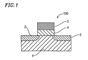
- Figure 1 is a cross-sectional view of a semiconductor memory device (also referred to as an "MFSFET device") 100 in a first example according to the present invention.
- MFSFET device semiconductor memory device
- the MFSFET device 100 includes a p-type Si substrate 1 having a source region 2 and a drain region 3 both of which are n + -type impurity regions and are at prescribed locations of a surface area of the p-type Si substrate 1 , a nitride ferroelectric layer 4 formed of Sr 2 NbN 3 provided on a prescribed area of the Si substrate 1 between the source region 2 and the drain region 3 , and a gate electrode 5 provided on the nitride ferroelectric layer 4 .
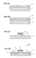
- Figure 2A through 2D are cross-sectional views illustrating the exemplary method for producing the MFSFET device 100
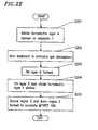
- Figure 2E is a flowchart illustrating the exemplary method.
- the p-type Si substrate 1 is first treated with a BHF (buffered fluoric acid) solution to remove a natural oxide layer (not shown) on a surface of the p-type Si substrate 1 .
- BHF buffered fluoric acid
- the resultant p-type Si substrate 1 is promptly introduced into a solution vaporization type plasma MOCVD (metal-organic chemical vapor deposition) apparatus 150 ( Figure 3 ) to form the nitride ferroelectric layer 4 formed of Sr 2 NbN 3 on the p-type Si substrate 1 to a thickness of, for example, about 200 nm (step S201 of Figure 2E ).
- MOCVD metal-organic chemical vapor deposition
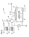
- FIG 3 is a schematic view of the solution vaporization type plasma MOCVD apparatus 150 .
- the solution vaporization type plasma MOCVD apparatus 150 includes a vacuum chamber 31 , which accommodates a heater 32 . As shown in Figure 3 , the p-type Si substrate 1 is placed on the heater 32 .
- the chamber 31 has an outlet 33 communicated with a pump (not shown) for vacuum-exhausting an internal gas.
- Reference numeral 34 represents a 13.56 MHz RF power supply for generating plasma.
- a liquid material 36 can be obtained by dissolving a solid material of Nb(O-iC 3 H 7 ) 4 (thd) in a THF (tetrahydrofuran) solvent.
- the liquid materials 35 and 36 are quantified by a liquid mass-flow controller 37 so that the molar ratio of Sr:Nb is 2:1, and transported to a vaporizer 38 .
- the liquid materials 35 and 36 are vaporized by the vaporizer 38 into a gas state and then introduced into a mixer 39 together with an N 2 gas acting as a carrier gas.
- the mixer 39 is located on the chamber 31 .
- the mixer 39 contains an NH 3 (ammonia) gas 41 introduced thereinto separately.
- the mixed gas of the gas-state materials 35 and 36 , the N 2 gas and the NH 3 gas 41 is directed to the p-type Si substrate 1 through a shower head 40 to generate plasma.
- the Sr and Nb are nitrided by ammonia plasma, and thus Sr 2 NbN 3 is formed on the p-type Si substrate 1 .
- the Sr 2 NbN 3 layer is formed under the conditions that the temperature of the p-type Si substrate 1 is about 550°C to about 650°C, the pressure is about 5 mm Torr to about 10 mm Torr and the RF power is about 100 W to about 150 W .
- the surface of the p-type Si substrate 1 is not oxidized, thus preventing formation of an SiO 2 film having a low dielectric constant at an interface between the p-type Si substrate 1 and the Sr 2 NbN 3 layer. Since Sr 2 NbN 3 does not include an element which is highly volatile and likely to react with Si, such as Pb or Bi, formation of an interface layer by diffusion of the elements of Sr 2 NbN 3 in the p-type Si substrate 1 is prevented.
- the Sr 2 NbN 3 layer is heat-treated in an electric oven at about 450°C for about 30 minutes in an ammonia gas atmosphere to improve the characteristics thereof (step S202 of Figure 2E ).
- the heat treatment can be performed using ammonia plasma or N 2 gas plasma, resulting in similar effects.
- the heat treatment process is performed in order to perfectly nitride the layer to improve the quality of the layer, but the advantages of the present invention are obtained even when the heat treatment is omitted.
- a TiN film 6 to be formed into the gate electrode 5 is formed by reactive sputtering using an Ar/N 2 mixed gas (step S203 of Figure 2E ).
- the TiN film 6 and the nitride ferroelectric layer 4 formed of Sr 2 NbN 3 are treated by etching to remove prescribed areas thereof, using a resist layer (step S204 of Figure 2E ).
- the etching is performed with, for example, an Ar/Cl 2 mixed gas.
- the nitride ferroelectric layer 4 formed of Sr 2 NbN 3 has a specific dielectric constant of about 13 and a spontaneous polarization value of as small as 1.0 ⁇ C/cm 2 , but the MFSFET device 100 is sufficiently operable at such a small residual polarization value.
- Figure 4 is a graph illustrating a C-V characteristic of the MFSFET device 100 .
- the C-V characteristic is measured under the conditions of ⁇ 5.0 V, 1 MHz and the gate area of 100 ⁇ m 2 .
- a memory window of about 1.6 V is obtained.
- the characteristic does not change even after the MFSFET device 100 is heat-treated with a hydrogen gas at about 450°C for about 30 minutes. This indicates that the MFSFET device 100 is stable against hydrogen gas sintering, etching using hydrogen, or metal or insulating film formation which are included in a usual Si-MOSFET process.
- the MFSFET device 100 includes the nitride ferroelectric layer 4 formed of Sr 2 NbN 3 .
- the MFSFET device according to the present invention can include a nitride ferroelectric layer formed of a material represented by formula (A x B 1-x ) z (C y D 1-y )N 3 (where x is in the range of 0 ⁇ x ⁇ 1, y is in the range of 0 ⁇ y ⁇ 1, A and B are each one element selected from the group consisting of Mg, Sr, Ba and Ca, and C and D are each one element selected from the group consisting of V, Nb, Ta and Mn).
- Such a material examples include Ba 2 TaN 3 , Ba 2 TiN 3 , and Sr 2 TaN 3 .
- Such a material is obtained by using Ba(thd) 2 , Mg(thd) 2 , Ca(thd) 2 or the like as the solid material in the liquid material 35 in place of Sr(thd) 2 , and using Ta(O-iC 3 H 7 ) 4 (thd), Mn(O-iC 3 H 7 ) 4 (thd) or the like as the solid material in the liquid material 36 in place of Nb(O-iC 3 H 7 ) 4 (thd).
- the resultant nitride ferroelectric layers have similar effects.
- FIG. 5 is a cross-sectional view of an MFSFET device 100A in a modification of the first example according to the present invention.
- the MFSFET device 100A includes a buffer layer 7 formed of a super-thin SiN film or SiO 2 film in addition to the structure shown in Figure 1 between the p-type Si substrate 1 and the nitride ferroelectric layer 4 formed of Sr 2 NbN 3 , for stabilizing the surface of the p-type Si substrate 1 .
- the buffer layer 7 can be formed by, for example, thermal oxidation or CVD.
- the nitride ferroelectric layer 4 formed of Sr 2 NbN 3 has a relatively low specific dielectric constant (about 13), an increase in the operating voltage is still suppressed even when the buffer layer 7 having a low specific dielectric constant (SiN: about 7; SiO 2 : about 4) is provided. thus, the MFSFET device 100A has improved stability.
- the molar ratio of Sr:Nb is set to 2:1 in the solution vaporization type plasma MOCVD apparatus 150 shown in Figure 3 .
- the molar ratio of Sr:Nb is set to 1:2, an SrNb 2 N 4 layer is obtained.
- the SrNb 2 N 4 layer has similar characteristics to those of the Sr 2 NbN 3 layer, but has a slightly lower specific dielectric constant (i.e., about 12) and a smaller spontaneous polarization value (i.e., 0.8 ⁇ C/cm 2 ).
- An MFSFET device including the SrNb 2 N 4 layer obtains a memory window of about 1.4 V under the same conditions as those for the measurement shown in Figure 4 .
- the MFSFET device can include a nitride ferroelectric layer formed of a material represented by formula (A x B 1-x )(C y D 1-y ) 2 N 4 (where x is in the range of 0 ⁇ x ⁇ 1, y is in the range of 0 ⁇ y ⁇ 1, A and B are each one element selected from the group consisting of Mg, Sr, Ba and Ca, and C and D are each one element selected from the group consisting of V, Nb, Ta and Mn). Examples of such a material include BaTa 2 N 4 , SrTa 2 N 4 , and BaNb 2 N 4 . Such materials are obtained by using different solid materials. The resultant nitride ferroelectric layers have similar effects.
- a x B 1-x )(C y D 1-y ) 2 N 4 (where x is in the range of 0 ⁇ x ⁇ 1, y is in the range of 0 ⁇ y ⁇ 1, A and B are each one element selected from the group consisting of Mg, Sr,
- the nitride ferroelectric film can be formed of the following exemplary materials, and the resultant ferroelectric layers have similar effects:
- the nitride ferroelectric layer 4 is formed by solution vaporization type plasma MOCVD.
- the nitride ferroelectric layer 4 can be formed by, for example, vacuum vapor deposition, MBE (molecular beam epitaxy), laser ablation, or reactive sputtering.
- the MFSFET device is described.
- the present invention is also applicable to an MFMIS (metal-ferroelectric-metal-insulator-semiconductor) FET devices including a floating gate electrode and an insulating layer below the ferroelectric layer.
- MFMIS metal-ferroelectric-metal-insulator-semiconductor
- Figure 6 is a cross-sectional view of an MFSFET device 200 in a second example according to the present invention. Identical elements as those described with reference to Figure 1 bear identical reference numerals and will not described in detail.
- the MFSFET device 200 includes a p-type Si substrate 1 having a source region 2 and a drain region 3 both of which are n + -type impurity regions and are at prescribed locations of a surface area of the p-type Si substrate 1 , a buffer layer 8 formed of a super-thin SiN film provided on a prescribed area of the Si substrate 1 between the source region 2 and the drain region 3 , a fluoride ferroelectric layer 9 formed of BaMgF 4 Provided on the buffer layer 8 , and a gate electrode 5 provided on the fluoride ferroelectric layer 9 .
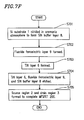
- Figure 7A through 7E are cross-sectional views illustrating the exemplary method for producing the MFSFET device 200
- Figure 7F is a flowchart illustrating the exemplary method.
- the p-type Si substrate 1 is treated with a BHF solution to remove a natural oxide layer (not shown) on a surface of the p-type Si substrate 1 .
- the resultant p-type Si substrate 1 is introduced into an RTA (rapid thermal anneal) apparatus (not shown) to perform direct nitriding (RTN: rapid thermal nitridation) of the p-type Si substrate 1 using an ammonia gas.
- RTA rapid thermal anneal
- RTA rapid thermal nitriding
- the buffer layer 8 formed of an SiN film having a thickness of, for example, about 10 nm is formed (step S701 of Figure 7F ).
- the nitride layer i.e., the buffer layer 8
- the thickness of the buffer layer 8 is preferably between about 5 nm to about 15 nm in consideration of the trade-off of the increase in the operating voltage of the MFSFET device 200 and the withstand voltage of the buffer layer 8 .
- the fluoride ferroelectric layer 9 formed of BaMgF 4 having a thickness of, for example, about 200 nm is formed by EB vacuum vapor deposition (step S702 of Figure 7F ).
- the fluoride ferroelectric layer 9 is formed under the conditions that the temperature of the p-type Si substrate 1 is about 600°C and BaF 2 and MgF 2 are used as vapor deposition sources.
- the vapor deposition rates of BaF 2 and MgF 2 are set so that the molar ratio of BaF 2 :MgF 2 is 1:1.
- a TiN film 6 to be formed into the gate electrode 5 is formed by reactive sputtering using an Ar/N 2 mixed gas (step S703 of Figure 7F ).
- the TiN film 6 and the fluoride ferroelectric layer 9 formed of BaMgF 4 are treated by etching to remove prescribed areas thereof, using a resist layer.
- the etching is performed with, for example, an Ar/Cl 2 mixed gas.
- the TiN film 6 becomes the gate electrode 5 as a result of etching.
- the buffer layer 8 formed of SiN is also etched using a resist layer and a CF 4 gas or the like (step S704 of Figure 7F ).
- the fluoride ferroelectric layer 9 formed of BaMgF 4 has a specific dielectric constant of about 10 and a spontaneous polarization value of 2.0 ⁇ C/cm 2 .
- the spontaneous polarization value is larger than that of the nitride ferroelectric layer 4 described in the first example.
- SiN used for forming the buffer layer 8 has a higher barrier characteristic than SiO 2 against the diffusion of fluorine which is contained in the BaMgF 4 used for forming the fluoride ferroelectric layer 9 in a large amount. Accordingly, SiN prevents the following phenomena deteriorating the MFSFET device 200 and thus improves the reliability of the MFSFET device 200 .
- SiN prevents the interface level from increasing by the diffusion of fluorine during heat treatment processes of, for example, formation of the BaMgF 4 layer, and ion implantation and annealing for activation of the p-type Si substrate 1.
- SiN prevents the thickness of the SiO 2 layer from increasing by the diffusion of oxygen which is released from the Si-O bond.
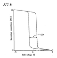
- Figure 8 is a graph illustrating a C-V characteristic of the MFSFET device 200 .
- the C-V characteristic is measured under the conditions of ⁇ 5.0 V, 1 MHz and the gate area of 100 ⁇ m 2 .
- a memory window of about 2.0 V is obtained.
- the operating voltage is suppressed from increasing even when the buffer layer 8 formed of SiN having a low specific dielectric constant (e.g., about 7) is included since the specific dielectric constant of the fluoride ferroelectric layer 9 formed of BaMgF 4 is relatively low (e.g., about 10).
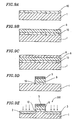
- Figure 9A through 9E are cross-sectional views illustrating an exemplary method for producing the MFSFET device 300
- Figure 9F is a flowchart illustrating the exemplary method. Identical elements as those described with reference to Figure 1 bear identical reference numerals and will not described in detail.
- the MFSFET device 300 includes a buffer layer 10 formed of an SiO 2 film having a nitrided surface in place of the buffer layer 8 formed of SiN.
- the p-type Si substrate 1 is treated with a BHF solution to remove a natural oxide layer (not shown) on a surface of the p-type Si substrate 1 .
- the resultant p-type Si substrate 1 is introduced into an RTA apparatus (not shown) to perform direct oxidation (RTO: rapid thermal oxidation) of the p-type Si substrate 1 using an oxygen gas.
- RTA direct oxidation
- an SiO 2 film having a thickness of, for example, about 10 nm is formed (step S901 of Figure 9F ).
- a surface of the SiO 2 film is nitrided using an N 2 gas or an ammonia gas, thereby forming the buffer layer 10 (step S902 of Figure 9F ).
- the SiO 2 film can be formed by thermal oxidation.
- the surface of the SiO 2 film can alternatively be nitrided by heat treatment using ammonia gas plasma or N 2 gas plasma, resulting in similar effects.
- a fluoride ferroelectric layer 9 formed of BaMgF 4 having a thickness of, for example, about 200 nm is formed by EB vacuum vapor deposition as shown in Figure 9B (step S903 of Figure 9F ).
- a TiN film 6 to be formed into the gate electrode 5 is formed by reactive sputtering using an Ar/N 2 mixed gas (step S904 of Figure 9F ).
- the TiN film 6 and the fluoride ferroelectric layer 9 formed of BaMgF 4 are treated by etching to remove prescribed areas thereof, using a resist layer. The etching is performed with, for example, an Ar/Cl 2 mixed gas.
- the TiN film 6 becomes the gate electrode 5 as a result of etching.
- the buffer layer 10 formed of SiO 2 is also etched using a resist layer and a CF 4 gas or the like (step S905 of Figure 9F ).
- As (arsenic) as an n-type impurity is implanted, and then the resultant body is annealed. As a result, the source region 2 and the drain region 3 are formed.
- the MFSFET device 300 is completed (step S906 of Figure 9F ).
- the SiO 2 film having a nitrided surface has a higher barrier characteristic than SiO 2 which is not nitrided against the diffusion of fluorine which is contained in the BaMgF 4 used for forming the fluoride ferroelectric layer 9 in a large amount. Accordingly, the buffer layer 10 improves the reliability of the MFSFET device 300 like the buffer layer 8 in the second example.
- FIG. 10A through 10F are cross-sectional views illustrating an exemplary method for producing the MFSFET device 400
- Figure 10G is a flowchart illustrating the exemplary method. Identical elements as those described with reference to Figure 1 bear identical reference numerals and will not described in detail.
- the MFSFET device 400 includes a p-type Si substrate 1 having a source region 2 and a drain region 3 both of which are n + -type impurity regions and are at prescribed locations of a surface area of the p-type Si substrate 1 , a buffer layer 8 formed of a super-thin SiN film provided on a prescribed area of the Si substrate 1 between the source region 2 and the drain region 3 , a ferroelectric layer 11 formed of BaMgF 4-x N 1/3x provided on the buffer layer 8 , and a gate electrode 5 provided on the ferroelectric layer 11 .
- the exemplary method for producing the MFSFET device 400 will be described.
- the p-type Si substrate 1 is treated with a BHF solution to remove a natural oxide layer (not shown) on a surface of the p-type Si substrate 1 .
- the resultant p-type Si substrate 1 is introduced into an RTA apparatus (not shown) to perform direct nitriding (RTN) of the p-type Si substrate 1 using an ammonia gas.
- RTA apparatus not shown
- RTN direct nitriding
- the buffer layer 8 formed of an SiN film having a thickness of, for example, about 10 nm is formed (step S1001 of Figure 10G ).
- the nitride layer i.e., the buffer layer 8
- the buffer layer can be formed by CVD.
- a fluoride ferroelectric layer 9 formed of BaMgF 4 having a thickness of, for example, about 200 nm is formed by EB vacuum vapor deposition (step S1002 of Figure 10G ).
- the fluoride ferroelectric layer 9 is formed under the conditions that the temperature of the p-type Si substrate 1 is about 600°C and BaF 2 and MgF 2 are used as vapor deposition sources.
- the vapor deposition rates of BaF 2 and MgF 2 are set so that the molar ratio of BaF 2 :MgF 2 is 1:1.
- the fluoride ferroelectric layer 9 is heat-treated in an electric oven at about 450°C for about 30 minutes in an ammonia gas atmosphere, thereby partially nitriding BaMgF 4 .
- the fluoride ferroelectric layer 9 becomes the ferroelectric layer 11 formed of BaMgF 4-x N 1/3x (0 ⁇ x ⁇ 4) partially including nitrogen ( N ), as shown in Figure 10C (step S1003 of Figure 10G ).
- the nitriding can alternatively be performed by heat treatment using ammonia gas plasma or N 2 gas plasma, resulting in similar effects.
- a TiN film 6 to be formed into the gate electrode 5 is formed by reactive sputtering using an Ar/N 2 mixed gas (step S1004 of Figure 10G ).
- the TiN film 6 and the ferroelectric layer 11 formed of BaMgF 4-x N 1/3x (0 ⁇ x ⁇ 4) are treated by etching to remove prescribed areas thereof, using a resist layer.
- the etching is performed with, for example, an Ar/Cl 2 mixed gas.
- the TiN film 6 becomes the gate electrode 5 as a result of etching.
- the buffer layer 8 formed of SiN is also etched using a resist layer and a CF 4 gas or the like (step S1005 of Figure 10G ).
- the ferroelectric layer 11 formed of BaMgF 4-x N 1/3x (0 ⁇ x ⁇ 4) has a specific dielectric constant of about 11, which is larger than that of the BaMgF 4 layer 9 .
- the spontaneous polarization value of the ferroelectric layer 11 is 1.5 ⁇ C/cm 2 , which is smaller than that of the BaMgF 4 layer 9 , the MFSFET device 400 is sufficiently operable.
- the ferroelectric layer 11 obtained by the nitriding suppresses the chemical reactivity of water and other substances, thus improving the stability of the MFSFET device 400 .
- the MFSFET device is described.
- the present invention is also applicable to an MFMIS FET devices including a floating gate electrode and an insulating layer below the ferroelectric layer.
- a BaMgF 4 is used as the fluoride ferroelectric material.
- BaCoF 4 , BaNiF 4 , and BaZnF 4 are usable, resulting in similar effects.
- Other usable fluoride ferroelectric materials include, for example, materials represented by formula (A x B 1-x )(C y D 1-y )F 5 (where x is in the range of 0 ⁇ x ⁇ 1, y is in the range of 0 ⁇ y ⁇ 1, A and B are each one element selected from the group consisting of Mg, Sr, Ba and Ca, and C and D are each one element selected from the group consisting of Al, Y, La, Sc, Co, Gd, Ce, Nd, Er, V, Ti, Ta, Nb and Mn), such as, for example, SrAlF 5 and SrTaF 5 ; materials represented by formula (A x B 1-x )(C y D 1-y )F 6 (where x is in the range of 0 ⁇ x ⁇ 1, y is in the range of 0 ⁇ y ⁇ 1, A and B are each one element selected from the group consisting of Mg, Sr, Ba and Ca, and C and D are each one element selected from the group consisting of Ti, Ta
- the fluoride ferroelectric layer is formed by EB vacuum vapor deposition.
- MOCVD, MBE, laser ablation, sputtering and the like are usable, resulting in similar effects.
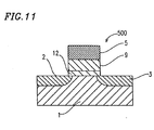
- FIG 11 is a cross-sectional view of a MFSFET device 500 in a fifth example according to the present invention. Identical elements as those described with reference to Figure 1 bear identical reference numerals and will not described in detail.
- the MFSFET device 500 includes a p-type Si substrate 1 having a source region 2 and a drain region 3 both of which are n + -type impurity regions and are at prescribed locations of a surface area of the p-type Si substrate 1 , a buffer layer 12 formed of MgSiO 3 provided on a prescribed area of the Si substrate 1 between the source region 2 and the drain region 3 , a fluoride ferroelectric layer 9 formed of BaMgF 4 provided on the buffer layer 12 , and a gate electrode 5 provided on the ferroelectric layer 9 .
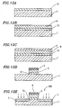
- Figure 12A through 12E are cross-sectional views illustrating an exemplary method for producing the MFSFET device 500
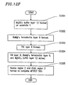
- Figure 12F is a flowchart illustrating the exemplary method.
- the p-type Si substrate 1 is treated with a BHF solution to remove a natural oxide layer (not shown) on a surface of the p-type Si substrate 1 .
- the buffer layer 12 formed of MgSiO 3 having a thickness of, for example, about 10 nm is formed on the p-type Si substrate 1 (step S1201 of Figure 12F ) by EB vacuum vapor deposition.
- the buffer layer 12 is formed under the conditions that the temperature of the p-type Si substrate 1 is about 600°C and MgO and SiO 2 are used as vapor deposition sources.
- the vapor deposition rates of MgO and SiO 2 are set so that the molar ratio of MgO:SiO 2 is 1:1.
- the buffer layer 12 is heat-treated in an electric oven at about 450°C for about 30 minutes in an oxygen gas or in an ozone-containing oxygen gas, thereby improving the interface characteristic of the buffer layer 12 .
- the fluoride ferroelectric layer 9 formed of BaMgF 4 having a thickness of, for example, about 200 nm is formed by EB vacuum vapor deposition (step S1202 of Figure 12F ).
- the fluoride ferroelectric layer 9 is formed under the conditions that the temperature of the p-type Si substrate 1 is about 600°C and BaF 2 and MgF 2 are used as vapor deposition sources.
- the vapor deposition rates of BaF 2 and MgF 2 are set so that the molar ratio of BaF 2 :MgF 2 is 1:1.
- a TiN film 6 to be formed into the gate electrode 5 is formed by reactive sputtering using an Ar/N 2 mixed gas (step S1203 of Figure 12F ).
- the TiN film 6 and the ferroelectric layer 9 formed of BaMgF 4 are treated by etching to remove prescribed areas thereof, using a resist layer.
- the etching is performed with, for example, an Ar/Cl 2 mixed gas.
- the TiN film 6 becomes the gate electrode 5 as a result of etching.
- the buffer layer 12 formed of MgSiO 3 is also etched using a resist layer and an Ar/Cl 2 /CF 4 mixed gas or the like (step S1204 of Figure 12F).
- MgSiO 3 used for the buffer layer 12 contains SiO 2 and Mg, which is an element of BaMgF 4 used for forming the fluoride ferroelectric layer 9 on the buffer layer 12 and thus has a satisfactory characteristic at the interface with the p-type Si substrate 1 .
- MgSiO 3 further has a very low reactivity with BaMgF 4 and improves the crystallinity of BaMgF 4 .
- the spontaneous polarization value of the fluoride ferroelectric layer 9 formed of BaMgF 4 is 2.6 ⁇ C/cm 2 , which is larger than that of the formed of fluoride ferroelectric layer 9 in the second example, which is also formed of BaMgF 4 .
- the buffer layer is formed of MgSiO 3 .
- the buffer layer can be formed of Mg 2 SiO 4 , SrSiO 3 , Sr 2 SiO 4 , (Mg x Sr 1-x )SiO 3 or (Mg x Sr 1-x ) 2 SiO 4 (0 ⁇ x ⁇ 1), resulting in similar effects.
- Mg 2 SiO 4 can be obtained by providing MgO and SiO 2 with the molar ratio of MgO:SiO 2 being 2:1.
- SrSiO 3 and Sr 2 SiO 4 can be obtained by using SrO and SiO 2 as the vapor deposition sources.
- (Mg x Sr 1-x )SiO 3 and (Mg x Sr 1-x ) 2 SiO 4 (0 ⁇ x ⁇ 1) can be obtained by using MgO, SrO and SiO 2 as the vapor deposition sources.
- the ferroelectric layer 9 and the buffer layer 12 both contain Sr and Mg; i.e., it is preferable that the ferroelectric layer 9 is formed of (Ba x Sr 1-x )MgF 4 or Ba(Mg x Sr 1-x )F 4 (0 ⁇ x ⁇ 1) and the buffer layer 12 is formed of (Mg x Sr 1-x )SiO 3 or (Mg x Sr 1-x ) 2 SiO 4 (0 ⁇ x ⁇ 1).
- FIG. 13A through 13F are cross-sectional views illustrating an exemplary method for producing the MFSFET device 600
- Figure 13G is a flowchart illustrating the exemplary method. Identical elements as those described with reference to Figure 1 bear identical reference numerals and will not described in detail.
- the MFSFET device 600 includes a p-type Si substrate 1 having a source region 2 and a drain region 3 both of which are n + -type impurity regions and are at prescribed locations of a surface area of the p-type Si substrate 1 , a buffer layer 8 formed of SiN provided on a prescribed area of the Si substrate 1 between the source region 2 and the drain region 3 , an SrTiO 3 layer 13 provided on the buffer layer 8 , a fluoride ferroelectric layer 9 formed of BaMgF 4 Provided on the SrTiO 3 layer 13 , and a gate electrode 5 provided on the ferroelectric layer 9 .
- the exemplary method for producing the MFSFET device 600 will be described.
- the p-type Si substrate 1 is treated with a BHF solution to remove a natural oxide layer (not shown) on a surface of the p-type Si substrate 1 .
- the resultant p-type Si substrate 1 is introduced into an RTA apparatus (not shown) to perform direct nitriding (RTN) of the p-type Si substrate 1 using an ammonia gas.
- RTA apparatus not shown
- RTN direct nitriding
- the buffer layer 8 formed of an SiN film having a thickness of, for example, about 5 nm is formed (step S1301 of Figure 13G ).
- the nitride layer i.e., the buffer layer 8
- the buffer layer 8 can be formed by CVD.
- the SrTiO 3 layer 13 having a thickness of, for example, about 30 nm is formed on the buffer layer 8 by reactive RF sputtering (step S1302 of Figure 13G ).
- the SrTiO 3 layer 13 is formed under the conditions that that the temperature of the p-type Si substrate 1 is about 350°C, the RF power is about 300 W, an SrTiO 3 target is used, and an Ar/O 2 mixed gas is used.
- the fluoride ferroelectric layer 9 formed of BaMgF 4 having a thickness of, for example, about 300 nm is formed by EB vacuum vapor deposition (step S1303 of Figure 13G ).
- the fluoride ferroelectric layer 9 is formed under the conditions that the temperature of the p-type Si substrate 1 is about 600°C and BaF 2 and MgF 2 are used as vapor deposition sources.
- the vapor deposition rates of BaF 2 and MgF 2 are set so that the molar ratio of BaF 2 :MgF 2 is 1:1.
- a TiN film 6 to be formed into the gate electrode 5 is formed by reactive sputtering using an Ar/N 2 mixed gas (step S1304 of Figure 13G ).
- the TiN film 6 , the ferroelectric layer 9 formed of BaMgF 4 and the SrTiO 3 layer 13 are treated by etching to remove prescribed areas thereof, using a resist layer.
- the etching is performed with, for example, an Ar/Cl 2 mixed gas (step S1305 of Figure 13G ).
- the MFSFET device 600 including the buffer layer 8 formed of SiN solves the following problem occurring in the Si/SiO 2 /SrTiO 3 structure.
- the SrTiO 3 target usually contains a high concentration of fluorine.
- the fluorine is diffused into the SiO 2 layer while the SrTiO 3 layer is formed by sputtering or during heat treatment processes, thereby cutting the Si-O bond.
- the Si-F bond is formed, thus increasing the interface level.
- Oxygen released from the Si-O bond is diffused into the Si/SiO 2 interface to form a new SiO 2 film. Accordingly, the thickness of the SiO 2 film is increased. This increases the operating voltage.
- SiN for the buffer layer 8 , the diffusion of fluorine is prevented, and thus the deterioration of the device characteristics is prevented.
- the buffer layer 8 is formed of SiN.
- the buffer layer 8 can be formed of an SiO 2 film having a surface nitrided by heat treatment, resulting in a similar effect of preventing the diffusion of fluorine.
- the heat treatment is performed in an RTA apparatus using, for example, ammonia gas, N 2 O gas or nitrogen radical ion-containing gas.
- the fluoride ferroelectric layer 9 is formed of BaMgF 4 .
- the ferroelectric layer can be formed of other fluoride ferroelectric materials or oxide ferroelectric materials such as, for example, PZT, SrBi 2 Ta 2 O 9 , and Bi 4 Ti 3 O 12 .
- the MFSFET device is described.
- the present invention is also applicable to an MFMIS FET devices including a floating gate electrode and an insulating layer below the ferroelectric layer.
- FIG. 14A through 14G are cross-sectional views illustrating an exemplary method for producing the MFSFET device 700
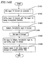
- Figure 14H is a flowchart illustrating the exemplary method. Identical elements as those described with reference to Figure 1 bear identical reference numerals and will not described in detail.
- the MFSFET device 700 includes a p-type Si substrate 1 having a source region 2 and a drain region 3 both of which are n + -type impurity regions and are at prescribed locations of a surface area of the p-type Si substrate 1 , an SrTiO 3 layer 13 provided on a prescribed area of the Si substrate 1 between the source region 2 and the drain region 3 , a fluoride ferroelectric layer 9 formed of BaMgF 4 provided on the SrTiO 3 layer 13 , and a gate electrode 5 provided on the ferroelectric layer 9 .
- the exemplary method for producing the MFSFET device 700 will be described.
- the p-type Si substrate 1 is treated with a BHF solution to remove a natural oxide layer (not shown) on a surface of the p-type Si substrate 1 .
- the resultant p-type Si substrate 1 is promptly introduced into an EB vacuum vapor deposition apparatus (not shown) to form a super thin TiSr layer 14 having a thickness of, for example, about 4 nm (step S1401 of Figure 14H ).
- the TiSr layer 14 is formed at room temperature, using Sr and Ti as vapor deposition sources. The vapor deposition rates of Sr and Ti are set so that the molar ratio of Sr:Tr is 1:1.
- the SrTiO 3 layer 13 having a thickness of, for example, about 30 nm is formed on the TiSr layer 14 by reactive RF sputtering using an SrtiO 3 target (step S1402 of Figure 14H ).
- the SrTiO 3 layer 13 is formed by a two-step method; i.e., an Ar gas is used to form the first 10 nm, and then an Ar/O 2 mixed gas is used to form the remaining 20 nm.
- the temperature of the p-type Si substrate 1 is preferably about 200°C to about 300°C, more preferably about 200°C to about 250°C, so that Ti and Sr deposited on the p-type Si substrate 1 do not react with Si.
- the RF power is about 100 W to about 250 W.
- the TiSr layer 14 is oxidized and incorporated into the SrTiO 3 layer 13 as shown in Figure 14C . It is preferable that the incorporation of the TiSr layer 14 into the SrTiO 3 layer 13 is substantially perfected, after the SrTiO 3 layer 13 is formed, by heat-treating the resultant body in an electric oven at about 200°C to about 250°C for about 30 minutes in an oxygen gas or an ozone-containing oxygen gas. This process is preferable to maintain the interface between the resultant SrTiO 3 layer 13 (after the TiSr layer 14 is incorporated) and the p-type Si substrate 1 stable in the heat treatment performed for forming the ferroelectric layer 9 .
- the fluoride ferroelectric layer 9 formed of BaMgF 4 having a thickness of, for example, about 300 nm is formed by EB vacuum vapor deposition (step S1403 of Figure 14H ) on the SrTiO 3 layer 13 .
- the fluoride ferroelectric layer 9 is formed under the conditions that the temperature of the p-type Si substrate 1 is about 600°C and BaF 2 and MgF 2 are used as vapor deposition sources.
- the vapor deposition rates of BaF 2 and MgF 2 are set so that the molar ratio of BaF 2 :MgF 2 is 1:1.
- a TiN film 6 to be formed into the gate electrode 5 is formed by reactive sputtering using an Ar/N 2 mixed gas (step S1404 of Figure 14H ).
- the TiN film 6 , the ferroelectric layer 9 formed of BaMgF 4 and the SrTiO 3 layer 13 are treated by etching to remove prescribed areas thereof, using a resist layer.
- the etching is performed with, for example, an Ar/Cl 2 mixed gas (step S1405 of Figure 14H ).
- the dielectric constant of the diode, including the p-type Si substrate 1 and the SrTiO 3 layer 13 , obtained based on the capacitance value of the diode is about 150 .
- the value of 150 is larger than the dielectric constant obtained when the SrTiO 3 13 is formed directly on the p-type Si substrate 1 without using the TiSr layer 14 (about 35). This indicates that the an SiO 2 film having a low specific dielectric constant is suppressed from being formed on the Si/SrTiO 3 interface.
- the SrTiO 3 layer 13 is formed by RF sputtering.
- the SrTiO 3 layer 13 can be formed by laser ablation which can form the layer at a temperature of about 300°C or less or vacuum vapor deposition, resulting in similar effects.
- the ferroelectric layer 9 is formed of BaMgF 4 .
- the ferroelectric layer can be formed of other fluoride ferroelectric materials or oxide ferroelectric materials such as, for example, PZT, SrBi 2 Ta 2 O 9 , and Bi 4 Ti 3 O 12 .
- the MFSFET device is described.
- the present invention is also applicable to an MFMIS FET devices including a floating gate electrode and an insulating layer below the ferroelectric layer.
- the gate electrode 5 is formed of TiN.
- the gate electrode can be formed of Pt or other appropriate materials.
- the MFSFET device includes the p-type Si substrate 1 .
- An n-type Si substrate can also be used.
- a stable and reliable semiconductor memory device which has satisfactory characteristics at the interface between the semiconductor substrate and the gate insulating layer formed of a nitride or fluoride ferroelectric material and can be produced using a general Si-MOSFET process; and a method for producing the same are provided.
Landscapes
- Semiconductor Memories (AREA)
- Non-Volatile Memory (AREA)
- Inorganic Compounds Of Heavy Metals (AREA)
- Physical Deposition Of Substances That Are Components Of Semiconductor Devices (AREA)
- Physical Vapour Deposition (AREA)
- Formation Of Insulating Films (AREA)
- Compounds Of Alkaline-Earth Elements, Aluminum Or Rare-Earth Metals (AREA)
Applications Claiming Priority (2)
| Application Number | Priority Date | Filing Date | Title |
|---|---|---|---|
| JP35750498 | 1998-12-16 | ||
| JP10357504A JP2000183295A (ja) | 1998-12-16 | 1998-12-16 | 半導体記憶装置及びその製造方法 |
Publications (2)
| Publication Number | Publication Date |
|---|---|
| EP1011149A2 true EP1011149A2 (de) | 2000-06-21 |
| EP1011149A3 EP1011149A3 (de) | 2000-09-27 |
Family
ID=18454465
Family Applications (1)
| Application Number | Title | Priority Date | Filing Date |
|---|---|---|---|
| EP99124901A Withdrawn EP1011149A3 (de) | 1998-12-16 | 1999-12-14 | Halbleiter-Speicheranordnung und Verfahren zur Herstellung |
Country Status (3)
| Country | Link |
|---|---|
| US (1) | US6380573B1 (de) |
| EP (1) | EP1011149A3 (de) |
| JP (1) | JP2000183295A (de) |
Cited By (2)
| Publication number | Priority date | Publication date | Assignee | Title |
|---|---|---|---|---|
| US6518634B1 (en) * | 2000-09-01 | 2003-02-11 | Motorola, Inc. | Strontium nitride or strontium oxynitride gate dielectric |
| WO2007010029A1 (fr) * | 2005-07-22 | 2007-01-25 | Commissariat A L'energie Atomique | Dispositif microelectronique dote de transistors surmontes d'une couche piezoelectrique |
Families Citing this family (6)
| Publication number | Priority date | Publication date | Assignee | Title |
|---|---|---|---|---|
| JP2001144087A (ja) | 1999-11-12 | 2001-05-25 | Natl Research Inst For Metals Ministry Of Education Culture Sports Science & Technology | 5族元素による酸化物/半導体界面の安定化方法と安定化半導体 |
| US6905920B2 (en) * | 2000-09-04 | 2005-06-14 | Seiko Epson Corporation | Method for fabrication of field-effect transistor to reduce defects at MOS interfaces formed at low temperature |
| JP4408787B2 (ja) * | 2004-10-19 | 2010-02-03 | 株式会社神戸製鋼所 | 絶縁膜及びその製造方法、並びに絶縁膜を備えた電子デバイス |
| US20060289948A1 (en) * | 2005-06-22 | 2006-12-28 | International Business Machines Corporation | Method to control flatband/threshold voltage in high-k metal gated stacks and structures thereof |
| KR20140146998A (ko) * | 2013-06-17 | 2014-12-29 | 전영권 | 태양전지 및 그 제조방법 |
| WO2021132602A1 (ja) * | 2019-12-27 | 2021-07-01 | 国立研究開発法人産業技術総合研究所 | 強誘電性薄膜、それを用いた電子素子および強誘電性薄膜の製造方法 |
Family Cites Families (8)
| Publication number | Priority date | Publication date | Assignee | Title |
|---|---|---|---|---|
| US4888246A (en) * | 1985-05-23 | 1989-12-19 | Matsushita Electric Industrial Co., Ltd. | Dielectric thin film, and method for making the thin film |
| JP3374216B2 (ja) * | 1991-10-26 | 2003-02-04 | ローム株式会社 | 強誘電体層を有する半導体素子 |
| EP0540993A1 (de) | 1991-11-06 | 1993-05-12 | Ramtron International Corporation | Struktur und Herstellung eines MOS-Feldeffekttransistors mit hoher Transkonduktanz unter Verwendung eines Gatedielektrikums, das aus einer übereinanderliegenden Pufferschicht/Ferroelektrikum/Pufferschicht besteht |
| US5442585A (en) * | 1992-09-11 | 1995-08-15 | Kabushiki Kaisha Toshiba | Device having dielectric thin film |
| US5439840A (en) * | 1993-08-02 | 1995-08-08 | Motorola, Inc. | Method of forming a nonvolatile random access memory capacitor cell having a metal-oxide dielectric |
| US5330931A (en) * | 1993-09-22 | 1994-07-19 | Northern Telecom Limited | Method of making a capacitor for an integrated circuit |
| JP3229911B2 (ja) * | 1994-08-12 | 2001-11-19 | シャープ株式会社 | 強誘電体記憶素子 |
| JPH08330531A (ja) | 1995-05-31 | 1996-12-13 | Sharp Corp | 強誘電体記憶素子 |
-
1998
- 1998-12-16 JP JP10357504A patent/JP2000183295A/ja active Pending
-
1999
- 1999-12-14 US US09/460,062 patent/US6380573B1/en not_active Expired - Lifetime
- 1999-12-14 EP EP99124901A patent/EP1011149A3/de not_active Withdrawn
Cited By (4)
| Publication number | Priority date | Publication date | Assignee | Title |
|---|---|---|---|---|
| US6518634B1 (en) * | 2000-09-01 | 2003-02-11 | Motorola, Inc. | Strontium nitride or strontium oxynitride gate dielectric |
| WO2007010029A1 (fr) * | 2005-07-22 | 2007-01-25 | Commissariat A L'energie Atomique | Dispositif microelectronique dote de transistors surmontes d'une couche piezoelectrique |
| FR2888990A1 (fr) * | 2005-07-22 | 2007-01-26 | Commissariat Energie Atomique | Dispositif microelectronique dote de transistors surmontes d'une couche piezoelectrique |
| US7968945B2 (en) | 2005-07-22 | 2011-06-28 | Commissariat A L'energie Atomique | Microelectronic device provided with transistors coated with a piezoelectric layer |
Also Published As
| Publication number | Publication date |
|---|---|
| US6380573B1 (en) | 2002-04-30 |
| EP1011149A3 (de) | 2000-09-27 |
| JP2000183295A (ja) | 2000-06-30 |
Similar Documents
| Publication | Publication Date | Title |
|---|---|---|
| US7135736B2 (en) | Semiconductor device | |
| US5619051A (en) | Semiconductor nonvolatile memory cell | |
| US6989573B2 (en) | Lanthanide oxide/zirconium oxide atomic layer deposited nanolaminate gate dielectrics | |
| US7157780B2 (en) | Semiconductor device and method for producing the same | |
| US7049192B2 (en) | Lanthanide oxide / hafnium oxide dielectrics | |
| US7396719B2 (en) | Method of forming high dielectric film using atomic layer deposition and method of manufacturing capacitor having the high dielectric film | |
| US8722484B2 (en) | High-K dielectric stack and method of fabricating same | |
| JP5650185B2 (ja) | 誘電体材料を含む個別要素又は半導体デバイスを含む集積回路デバイス | |
| EP1265279A1 (de) | Flash-speicherbaustein und verfahren zu seiner herstellung und verfahren zur ausbildung eines dielektrischen films | |
| US20060261397A1 (en) | Lanthanide oxide/hafnium oxide dielectric layers | |
| KR19990068059A (ko) | 금속 산화물 반도체 실리콘 소자 제조 방법 | |
| KR20170121082A (ko) | 반도체 강유전체 기억소자의 제조방법 및 반도체 강유전체 기억 트랜지스터 | |
| US7495264B2 (en) | Semiconductor device with high dielectric constant insulating film and manufacturing method for the same | |
| US7419918B2 (en) | Methods of forming a thin-film structure, methods of manufacturing non-volatile semiconductor devices using the same, and resulting non-volatile semiconductor devices | |
| EP1011149A2 (de) | Halbleiter-Speicheranordnung und Verfahren zur Herstellung | |
| US6503763B2 (en) | Method of making MFMOS capacitors with high dielectric constant materials | |
| US7527982B1 (en) | Manufacturing method of a semiconductor device including a crystalline insulation film made of perovskite type oxide | |
| KR0151241B1 (ko) | 강유전체막을 구비한 반도체장치 | |
| US8691647B1 (en) | Memory devices containing a high-K dielectric layer | |
| JP2003188356A (ja) | 金属、絶縁膜、強誘電体膜積層構造とその製造方法 | |
| JP3813206B2 (ja) | 強誘電体記憶素子の製造方法 | |
| Eom et al. | Changes in structures and electrical conduction mechanisms of chemical vapor deposited Ta2O5 thin films by annealing under O3 atmosphere with ultraviolet light radiation | |
| Ohtsubo et al. | Thin SiON Film Grown at Low Temperature (400$^ circhboxC $) by Microwave-Excited High-Density $ hboxKr/hboxO_2/hboxN_2 $ Plasma | |
| JPH1126704A (ja) | 強誘電体記憶素子 | |
| Kim | Performance and reliability of insulator for nanometer metal-insulator-semiconductor field effects transistors |
Legal Events
| Date | Code | Title | Description |
|---|---|---|---|
| PUAI | Public reference made under article 153(3) epc to a published international application that has entered the european phase |
Free format text: ORIGINAL CODE: 0009012 |
|
| AK | Designated contracting states |
Kind code of ref document: A2 Designated state(s): DE FR GB IT NL |
|
| AX | Request for extension of the european patent |
Free format text: AL;LT;LV;MK;RO;SI |
|
| PUAL | Search report despatched |
Free format text: ORIGINAL CODE: 0009013 |
|
| AK | Designated contracting states |
Kind code of ref document: A3 Designated state(s): AT BE CH CY DE DK ES FI FR GB GR IE IT LI LU MC NL PT SE |
|
| AX | Request for extension of the european patent |
Free format text: AL;LT;LV;MK;RO;SI |
|
| 17P | Request for examination filed |
Effective date: 20001004 |
|
| AKX | Designation fees paid |
Free format text: DE FR GB IT NL |
|
| RAP1 | Party data changed (applicant data changed or rights of an application transferred) |
Owner name: MATSUSHITA ELECTRIC INDUSTRIAL CO., LTD. |
|
| STAA | Information on the status of an ep patent application or granted ep patent |
Free format text: STATUS: THE APPLICATION IS DEEMED TO BE WITHDRAWN |
|
| 18D | Application deemed to be withdrawn |
Effective date: 20060719 |