EP1014428A2 - Condensateur pour circuit intégré - Google Patents
Condensateur pour circuit intégré Download PDFInfo
- Publication number
- EP1014428A2 EP1014428A2 EP99309388A EP99309388A EP1014428A2 EP 1014428 A2 EP1014428 A2 EP 1014428A2 EP 99309388 A EP99309388 A EP 99309388A EP 99309388 A EP99309388 A EP 99309388A EP 1014428 A2 EP1014428 A2 EP 1014428A2
- Authority
- EP
- European Patent Office
- Prior art keywords
- electrode
- layer
- capacitor
- integrated circuit
- area
- Prior art date
- Legal status (The legal status is an assumption and is not a legal conclusion. Google has not performed a legal analysis and makes no representation as to the accuracy of the status listed.)
- Withdrawn
Links
Images

Classifications
-
- H—ELECTRICITY
- H10—SEMICONDUCTOR DEVICES; ELECTRIC SOLID-STATE DEVICES NOT OTHERWISE PROVIDED FOR
- H10D—INORGANIC ELECTRIC SEMICONDUCTOR DEVICES
- H10D1/00—Resistors, capacitors or inductors
- H10D1/60—Capacitors
- H10D1/68—Capacitors having no potential barriers
-
- H—ELECTRICITY
- H10—SEMICONDUCTOR DEVICES; ELECTRIC SOLID-STATE DEVICES NOT OTHERWISE PROVIDED FOR
- H10D—INORGANIC ELECTRIC SEMICONDUCTOR DEVICES
- H10D84/00—Integrated devices formed in or on semiconductor substrates that comprise only semiconducting layers, e.g. on Si wafers or on GaAs-on-Si wafers
- H10D84/80—Integrated devices formed in or on semiconductor substrates that comprise only semiconducting layers, e.g. on Si wafers or on GaAs-on-Si wafers characterised by the integration of at least one component covered by groups H10D12/00 or H10D30/00, e.g. integration of IGFETs
- H10D84/811—Combinations of field-effect devices and one or more diodes, capacitors or resistors
- H10D84/817—Combinations of field-effect devices and resistors only
Definitions
- This invention relates to capacitors on integrated circuits (ICs).
- Integrated circuits often have IC capacitors using MOS transistor channel capacitance. These MOS structures provide limited capacitance for two reasons. First, capacitance per unit area is small. Second, limited die area is available. Capacitance size remains limited in part because both chip failure rates and production costs increase as chip area increases.
- the present invention therefore seeks to provide for an integrated circuit capacitor exhibiting an advantage over known such capacitors.
- an integrated circuit including a substrate having a principal surface, one or more device areas defined on said substrate principal surface, an interconnect area laterally adjacent to said one or more device areas, and having one or more interconnects that electrically connect to said one or more device areas and overlie said interconnect area, and a capacitor, the capacitor comprising a first electrode overlying said substrate principal surface and vertically coextensive at least in part with the said interconnect area, a dielectric layer overlying said first electrode, and a second electrode overlying the said dielectric layer.
- a method of forming a capacitor on an integrated circuit having a substrate with a principal surface and with one or more device areas defined laterally on the said principal surface, an interconnect area being laterally adjacent to the said one or more device areas, the method comprising the steps of forming a first electrode overlying the said principal surface and vertically coextensive at least in part with said interconnect area, forming a dielectric layer overlying the said first electrode, and forming a second electrode overlying the said dielectric layer.
- Integrated circuit chips having large numbers of logic circuits typically employ logic cell configurations that are placed in rows and interconnected using techniques involving computer programs. Such chips generally require a large chip surface area for the interconnect wiring. Thus a large chip surface area lies otherwise unused under a chip's interconnect areas.
- This invention uses that area, vertically coextensive (e.g., under at least in part) with a chip's interconnect area, to form therein large capacitors.
- the chip surface area under the so-called "random" interconnect wiring on other portions of the chip is also available.
- a first polysilicon electrode layer is deposited to form a first capacitor electrode.
- a dielectric layer is then deposited overlying the first electrode.
- a second polysilicon electrode layer is deposited overlying the dielectric layer, followed by an overlying insulating layer.
- conventional device interconnects are formed overlying the insulating layer.
- the polysilicon, dielectric, and insulating layers are those also used to define other conventional on-chip structures (e.g. floating gate and/or standard transistors) so that no additional processing steps are necessary to define the capacitors.
- the capacitor layers and corresponding transistor gate structure layers are laterally coextensive, meaning that while they are not necessarily exactly physically aligned laterally, they are formed by the same process steps.
- chip surface area used by these capacitors is thus “free” since it is already allocated to the overlying interconnects, and so is available at no additional cost in terms of chip surface area.
- the chip area employed for the wiring thereby provides double duty by allowing "interpoly" capacitors to be buried beneath the multilayer metal interconnect wiring.
- Application-specific non-volatile memories are one such application area since they usually contain large sections of digital logic employing extensive interconnect.
- VDD (power) and VSS (ground) wiring typically is interspersed in such interconnect, such distributed interpoly filter capacitors readily can be coupled to the VDD bus. In this manner, distributed filter capacitors with total size of e.g. many hundreds of picofarads can be realized with negligible increase in chip area and with no process change.
- capacitors formed underlying interconnect areas are electrically connected so as to increase total capacitance. Some embodiments also electrically connect one or more of the capacitors between the chip power supply terminals as filter capacitors. In still other embodiments the on-chip capacitance is large enough to store and filter a weak charge replenished by an external RF field, to power the IC.
- Integrated circuits (ICs) having extensive interconnect wiring require that a considerable chip surface area be devoted to that wiring.
- ICs that require large capacitors also require a considerable chip surface area be used for the capacitors.
- This invention is directed to using the same vertically coextensive chip area for both the on-chip capacitors and interconnect wiring.
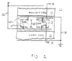
- Fig. 1 is a plan view of a part of a surface of an integrated circuit showing, in accordance with an embodiment of the invention, a capacitor formed underlying integrated circuit device wiring.
- conventional device logic cell area 12 is shown positioned on an IC surface 10.
- An interconnect area 14 (hatched) is adjacent device cell area 12 (which conventionally includes a large number of transistors connected to form logic gates).
- Cell area 12 is e.g. a "standard cell" or other logic cell of the type well known in the IC field.
- interconnect wiring occupies interconnect area 14 so as to conventionally electrically interconnect the device cell area 12 to other cells and/or to other integrated circuit devices (not shown).
- An optional conventional power bus area (VDD) 16 is shown (schematically) adjacent the device cell area 12.
- An optional conventional ground bus (VSS) 18 is also shown schematically. Power bus 16 and ground bus 18 conventionally provide respectively a power source and ground reference for circuit devices attached thereto.
- a conventional memory e.g. EEPROM or EPROM cell area 15 positioned laterally to interconnect area 14. It is to be understood that the particular layout of FIG. 1 is only illustrative.
- Two capacitor areas 20a and 20b are shown within interconnect area 14.
- the dashed lines represent that capacitor areas 20a, 20b are located underneath the interconnect wiring (not shown) with respect to the IC substrate in interconnect area 14.
- connections 22a and 22b between each capacitor area and power bus 16, and connections 24a and 24b between each capacitor area and ground bus 18.
- Connections 22a, 22b and 24a, 24b are to, respectively, the two electrodes of the capacitors in areas 20a, 20b.
- Area 26 between the two capacitor areas 20a and 20b represents an example of an area in which multi-level interconnect wiring (not shown) density precludes forming an underlying (buried) capacitor.
- the area available to form such capacitors underlying interconnect wiring varies with the nature and extent of the wiring. Other embodiments may therefore allow more or less capacitor area than that shown in this depiction.
- the capacitor is not limited to being formed between device cells such as cell areas 12 and 15.
- the interconnect area under which the capacitors are located is at other regions of the chip, for instance under so-called "random" interconnect areas.
- the power bus area 16 and ground bus area 18 are some common interdevice connection on the integrated circuit other than a power or ground source or reference, or are omitted entirely.
- FIG. 2 shows a cross-section corresponding to portions of a capacitor and active devices intersected by cut line A-A in FIG. 1. Structures in FIG. 2 having the same reference numbers as in FIG. 1 refer to the same structures.
- One illustrative conventional floating gate transistor 34 is shown formed on IC substrate 30 (having surface 10) in cell area 15. The doped portions of transistor 34 (source/drain regions) in substrate 30 are 47, 49, respectively.
- the conventional source/drain and gate contacts are 58a, 58b, 58c.
- a first (lower) planar capacitor electrode 38 is shown in interconnect area 14, overlaid by a dielectric layer 40.
- a second planar capacitor electrode 42 is shown overlying first electrode 38.
- An insulating layer 44 e.g. BPSG (borophosphosilicate glass) overlies second electrode 42, and a conductive interconnect layer 46 overlies insulating layer 44.
- FIG. 2 shows how the capacitor layers are formed by the same process steps as the corresponding (laterally coextensive) floating gate transistor 34 gate structure layers.
- floating gate dual gate
- EPROM non-volatile memory
- Other standard (single gate layer) logic transistors are formed in the same process steps but omit one gate electrode layer and the inter-gate dielectric layer.
- One such standard transistor 43 is depicted in FIG. 2 in logic cell area 12.
- the composition of conventional gate oxide layer 45, capacitor electrodes 38 and 42, dielectric 40, insulating layer 44, and conductive interconnect 46 may vary.
- the embodiment shown has materials and structures compatible with those used to form IC MOS transistors, as discussed below. Hence these capacitors can be formed in the same conventional process steps as the gate structures of the transistors with which they are laterally coextensive, as in FIG. 2. Those skilled in the art will understand, however, that the capacitors may use many different compositions having desired electrical properties.
- FIG. 2 thus illustrates in cross section both the buried capacitor and exemplary active circuit devices formed by the same conventional process steps.
- the sequence of steps is apparent to one of ordinary skill in the art.
- the embodiment shown uses conventional doped polysilicon transistor gate electrode and dielectric layers to define the capacitor.
- the first capacitor electrode 38 is a polysilicon (polycrystalline silicon) layer formed in the same step(s) as is the floating gate electrode 50 which is a conventional polysilicon layer ("poly-1") in transistor 34.
- a single deposited polysilicon layer (“poly-2”) defines both second capacitor electrode 42 and conventional gate electrode 54.
- the same insulating layer defines dielectric layer 40 between electrodes 38 and 42, and corresponding inter-gate insulating layer 52 located between the two transistor gate electrodes 50 and 54.
- layer 40 and 52 is conventional silicon dioxide (SiO 2 ).
- An alternative material for layer 40 and 52 is the well known "ONO" (silicon dioxide-silicon nitride-silicon dioxide) stack.
- An additional conventional SiO 2 or BPSG layer may then form layers 44 and 56.
- transistor 34 includes doped (source/drain) regions 51, 53, gate oxide layer 45, and gate electrode 70.
- Contacts 62a, 62b, 62c are conventional.
- a conductive layer such as aluminum is deposited and patterned to form both transistor contacts 58a, 58b, 58c and 60a, 60b, 60c and required wiring in interconnect area 32 as represented by conductive interconnect 46.
- conductive interconnect 46 may be present separated by intervening insulative layers.
- all process steps are conventional IC (e.g. CMOS) process steps, yet no extra process steps are required to form the capacitor. It is to be understood that the masks used in these fabrication steps to define the transistor structures are configured so as also to define the corresponding capacitor structures.
Landscapes
- Semiconductor Integrated Circuits (AREA)
- Design And Manufacture Of Integrated Circuits (AREA)
Applications Claiming Priority (2)
| Application Number | Priority Date | Filing Date | Title |
|---|---|---|---|
| US21199598A | 1998-12-14 | 1998-12-14 | |
| US211995 | 1998-12-14 |
Publications (2)
| Publication Number | Publication Date |
|---|---|
| EP1014428A2 true EP1014428A2 (fr) | 2000-06-28 |
| EP1014428A3 EP1014428A3 (fr) | 2001-12-12 |
Family
ID=22789112
Family Applications (1)
| Application Number | Title | Priority Date | Filing Date |
|---|---|---|---|
| EP99309388A Withdrawn EP1014428A3 (fr) | 1998-12-14 | 1999-11-24 | Condensateur pour circuit intégré |
Country Status (1)
| Country | Link |
|---|---|
| EP (1) | EP1014428A3 (fr) |
Family Cites Families (2)
| Publication number | Priority date | Publication date | Assignee | Title |
|---|---|---|---|---|
| US5814850A (en) * | 1995-08-22 | 1998-09-29 | Nippon Steel Corporation | Semiconductor device including a capacitor responsible for a power supply voltage to semiconductor device and capable of blocking an increased voltage |
| US5908311A (en) * | 1996-07-25 | 1999-06-01 | National Semiconductor Corporation | Method for forming a mixed-signal CMOS circuit that includes non-volatile memory cells |
-
1999
- 1999-11-24 EP EP99309388A patent/EP1014428A3/fr not_active Withdrawn
Also Published As
| Publication number | Publication date |
|---|---|
| EP1014428A3 (fr) | 2001-12-12 |
Similar Documents
| Publication | Publication Date | Title |
|---|---|---|
| KR100787664B1 (ko) | 반도체 장치 | |
| KR100544943B1 (ko) | 반도체 집적회로장치 및 그 제조방법 | |
| US6124163A (en) | Integrated chip multiplayer decoupling capacitors | |
| US20040140527A1 (en) | Semiconductor device having poly-poly capacitor | |
| JPH021928A (ja) | 半導体集積回路 | |
| KR100843272B1 (ko) | 반도체 집적회로장치 | |
| US8050066B2 (en) | MISFET with capacitors | |
| US6476459B2 (en) | Semiconductor integrated circuit device with capacitor formed under bonding pad | |
| JPH09116027A (ja) | 半導体装置及びその製造方法 | |
| US6384454B2 (en) | Process for manufacturing integrated circuit SRAM | |
| US6781869B2 (en) | Semiconductor memory | |
| US7030030B2 (en) | Method of manufacturing a semiconductor integrated circuit device having a plurality of wiring layers and mask-pattern generation method | |
| US7462523B2 (en) | Semiconductor memory device and method for manufacturing the same | |
| JPH07235616A (ja) | 半導体装置および半導体装置の製造方法 | |
| US6583492B2 (en) | Capacitor element having a contact hole structure in an electrode structure | |
| US6627970B2 (en) | Integrated semiconductor circuit, in particular a semiconductor memory circuit, having at least one integrated electrical antifuse structure, and a method of producing the structure | |
| EP1014428A2 (fr) | Condensateur pour circuit intégré | |
| US6437394B1 (en) | Non-volatile semiconductor memory device with reduced line resistance and method of manufacturing | |
| JP2001177056A (ja) | 半導体集積回路装置 | |
| KR100649067B1 (ko) | Mis 커패시터 및 mis 커패시터 제조 방법 | |
| US20100258850A1 (en) | Semiconductor integrated device | |
| US6815748B2 (en) | Semiconductor integrated circuit device with connections formed using a conductor embedded in a contact hole | |
| JP3254549B2 (ja) | 半導体装置及びその製造方法 |
Legal Events
| Date | Code | Title | Description |
|---|---|---|---|
| PUAI | Public reference made under article 153(3) epc to a published international application that has entered the european phase |
Free format text: ORIGINAL CODE: 0009012 |
|
| AK | Designated contracting states |
Kind code of ref document: A2 Designated state(s): AT BE CH CY DE DK ES FI FR GB GR IE IT LI LU MC NL PT SE |
|
| AX | Request for extension of the european patent |
Free format text: AL;LT;LV;MK;RO;SI |
|
| PUAL | Search report despatched |
Free format text: ORIGINAL CODE: 0009013 |
|
| AK | Designated contracting states |
Kind code of ref document: A3 Designated state(s): AT BE CH CY DE DK ES FI FR GB GR IE IT LI LU MC NL PT SE |
|
| AX | Request for extension of the european patent |
Free format text: AL;LT;LV;MK;RO;SI |
|
| AKX | Designation fees paid | ||
| REG | Reference to a national code |
Ref country code: DE Ref legal event code: 8566 |
|
| STAA | Information on the status of an ep patent application or granted ep patent |
Free format text: STATUS: THE APPLICATION IS DEEMED TO BE WITHDRAWN |
|
| 18D | Application deemed to be withdrawn |
Effective date: 20020613 |