EP1014448A2 - Nichtflüchtiges Halbleiterspeicherbauelement und dessen Herstellungsverfahren - Google Patents
Nichtflüchtiges Halbleiterspeicherbauelement und dessen Herstellungsverfahren Download PDFInfo
- Publication number
- EP1014448A2 EP1014448A2 EP99125534A EP99125534A EP1014448A2 EP 1014448 A2 EP1014448 A2 EP 1014448A2 EP 99125534 A EP99125534 A EP 99125534A EP 99125534 A EP99125534 A EP 99125534A EP 1014448 A2 EP1014448 A2 EP 1014448A2
- Authority
- EP
- European Patent Office
- Prior art keywords
- insulating film
- drain
- memory cell
- source
- gate
- Prior art date
- Legal status (The legal status is an assumption and is not a legal conclusion. Google has not performed a legal analysis and makes no representation as to the accuracy of the status listed.)
- Withdrawn
Links
Images


Classifications
-
- H—ELECTRICITY
- H10—SEMICONDUCTOR DEVICES; ELECTRIC SOLID-STATE DEVICES NOT OTHERWISE PROVIDED FOR
- H10B—ELECTRONIC MEMORY DEVICES
- H10B69/00—Erasable-and-programmable ROM [EPROM] devices not provided for in groups H10B41/00 - H10B63/00, e.g. ultraviolet erasable-and-programmable ROM [UVEPROM] devices
-
- H—ELECTRICITY
- H10—SEMICONDUCTOR DEVICES; ELECTRIC SOLID-STATE DEVICES NOT OTHERWISE PROVIDED FOR
- H10B—ELECTRONIC MEMORY DEVICES
- H10B41/00—Electrically erasable-and-programmable ROM [EEPROM] devices comprising floating gates
- H10B41/30—Electrically erasable-and-programmable ROM [EEPROM] devices comprising floating gates characterised by the memory core region
Definitions
- This invention relates to a semiconductor device and a method of manufacturing the same, and more particularly to the suppression of overetching occurred in element isolating regions in making contact holes.
- STI Shallow Trench Insulation
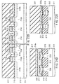
- FIG. 1 is a sectional view of a semiconductor device in which such penetration has occurred.
- a trench 3 is formed in a semiconductor substrate 2.
- an element isolation insulating film 4 is embedded.
- the trench 3 and element isolation insulating film 4 constitute an STI.
- the STI delimits an element region in which an element is to be formed.
- a transistor has been formed.
- the transistor is composed of a gate electrode structure including a gate insulating film 5, a floating gate 6, a gate-to-gate insulating film 7, and a control gate 8, and a source/drain region (diffused layer) 9 formed in the element region excluding the portion under the gate electrode structure.
- an interlayer insulating film 22 On the substrate having the element region in which the STI and a memory cell have been formed, an interlayer insulating film 22 has been formed. In the interlayer insulating film 22, a contact hole 26 leading to the source/drain region 9 has been formed.
- a resist pattern 24 of photoresist with openings according to the opening pattern of the contact hole 26 is formed on the interlayer insulating film 22. Thereafter, with the resist pattern 24 as a mask, the interlayer insulating film 22 is etched using RIE (reactive ion etching) techniques. In this way, the contact hole 26 is made in the interlayer insulating film 22.
- RIE reactive ion etching
- the contact hole 26 comes off the source/drain region 9 and overlaps with the STI, however, the element isolation insulating film 4 is etched and the contact hole 26 penetrates through the side face or underside of the trench 3 to the substrate 2.
- a buffer insulating film 10 made of buffer material e.g., silicon oxide
- a barrier insulating film 12 made of, for example, silicon nitride is formed all over the surface above the substrate 2 as shown in FIG. 2A.
- Silicon nitride has an etching selectivity to silicon oxide.
- an interlayer insulating film 22 made of silicon oxide is formed on the interlayer insulating film 22, a resist pattern 24 is formed. Thereafter, with the resist pattern 24 as a mask, the interlayer insulating film 22 is etched using RIE techniques, thereby making the contact hole 26 reaching the barrier insulating film 12.
- the barrier insulating film 12 and the buffer insulating film 10 under the barrier insulating film 12 are etched by RIE using the resist pattern 24 as a mask, which thereby makes the contact hole 26 that reaches the source/drain region 9.
- the barrier insulating film 12 As described above, forming the barrier insulating film 12 all over the surface above the substrate 2 prevents the penetration.
- the barrier insulating film 12 also helps prevent contamination from the outside.
- FIG. 4 shows a current-voltage characteristic diagram of the conventional transistor, particularly the relationship between the drain current I D and the voltage V G of the control gate 8.
- curve G1 is a current-voltage characteristic curve of the transistor in the initial state (before the repetition of writing and erasing) and curve G2 is a current-voltage characteristic curve of the transistor after the writing and erasing have been done repeatedly.
- an object of the present invention to provide a semiconductor device capable of preventing a decrease in the reliability as much as possible and a method of manufacturing the semiconductor device.
- a semiconductor device comprising: a semiconductor substrate having an element isolating region and an element formation region; a transistor having a first and a second diffused layer formed in the element formation region and a gate electrode structure formed on the element formation region between the first and second diffused layers; and a barrier insulating film formed above the semiconductor substrate excluding the vicinity of the gate electrode structure.
- the barrier insulating film since the barrier insulating film has been formed above the substrate excluding the vicinity of the gate electrode structure of the transistor, the barrier insulating film is prevented from being charged. Consequently, the diffused layers in the transistor never turn to depletion layers, which prevents the on current in the transistor from decreasing.
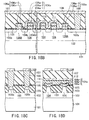
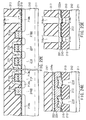
- FIG. 5 is a sectional view of a semiconductor device according to a first embodiment of the present invention.
- an element isolating shallow trench 3 is formed in a p-type silicon substrate 2, an element isolating shallow trench 3 is formed.
- an element isolation insulating film 4 is embedded.
- the shallow trench 3 and element isolation insulating film 4 constitute an STI, which delimits an element region in which an element is to be formed, at the surface of the substrate 2.
- a transistor has been formed.
- the transistor is composed of a gate electrode structure including a gate insulating film 5, a floating gate 6, a gate-to-gate insulating film 7, and a control gate 8, and a source/drain region, such as an n-type diffused layer 9, formed in the element region excluding the portion under the gate electrode structure.
- an insulating film 10 made of buffer material e.g., silicon oxide
- a barrier insulating film 12 made of silicon nitride has been formed on the portion of the insulating film 10 excluding the vicinity of the gate electrode structure.
- the barrier insulating film 12 remains on the element isolation insulating film 4 adjacent to a contact formation region (or the diffused layer 9 in the first embodiment).
- the barrier insulating film 12 since the barrier insulating film 12 has not been formed in the vicinity of the gate electrode structure, even if data is written and deleted repeatedly, a part of the diffused layer 9 will not turn to a depletion layer. Thus, it is possible to prevent the drain current (on current) in the transistor from decreasing, which prevents a decrease in the reliability as mush as possible.
- FIG. 6 is a sectional view showing an important manufacturing process of a semiconductor device according to the first embodiment.
- a shallow trench 3 is formed in the region in which an element isolating region is to be formed, in, for example, a p-type silicon substrate 2. Then, the shallow trench 3 is filled with the element isolation insulating film 4 made of silicon oxide. Then, on the entire surface of the substrate 2, a gate insulating film 5, a conductive film 6 to act as a floating gate, an insulating film 7, and a conductive film 8 to act as a control gate are stacked one on top of another in that order. Patterning these films produces a gate electrode structure.
- n-type impurity ions are implanted into the portions corresponding to both sides of the gate electrode structure, thereby forming a diffused layer 9 to act as a source and a drain.
- a buffer insulating film 10 made of silicon oxide has been formed on the entire surface of the substrate 2
- a barrier insulating film 12 made of silicon nitride is formed.
- a resist pattern 14 made of photoresist with an opening near the gate electrode structure is formed on the barrier insulating film 12.
- the barrier insulating film 12 is etched by isotropic dry etching or RIE. In this way, the barrier insulating film 12 is removed from the vicinity of the gate electrode structure. The barrier insulating film is left on the element isolation insulating film 4 adjacent to the contact formation region.
- annealing is done to improve the quality of the buffer insulating film 10. Then, annealing is done to activate the diffused layer 9, thereby producing a semiconductor device shown in FIG. 5.
- an interlayer insulating film (not shown) is formed all over the surface above the substrate 2. Then, a contact hole (not shown) is made in the interlayer insulating film. Following that, the contact hole is filled with conductive material, thereby forming a contact (not shown) made of the conductive material within the contact hole.
- a second embodiment of the present invention relates to a method of manufacturing semiconductor devices.
- FIGS. 7A and 7B are sectional views showing manufacturing processes to help explain a method of manufacturing a semiconductor device according to the second embodiment.
- the component elements up to the barrier insulating film 12 have been formed all over the surface above the substrate 2.
- a silicon oxide film 13 is formed on the barrier insulating film 12. Then, on the silicon oxide film 13, a resist pattern 14 made of photoresist with an opening near the gate electrode structure is formed. Following that, using the resist pattern 14 as a mask, the barrier insulating film 12 is etched by dry etching or wet etching.
- the barrier insulating film 12 is removed from the vicinity of the gate electrode structure using hot phosphoric acid solution, with the silicon oxide film 13 as a mask.
- the barrier insulating film 12 is left on the element isolation insulating film 4 adjacent to the contact formation region.
- an interlayer insulating film (not shown) is formed all over the surface above the substrate 2. Then, a contact hole (not shown) is made in the interlayer insulating film. Following that, the contact hole is filled with conductive material, thereby forming a contact (not shown) made of the conductive material within the contact hole.
- the barrier insulating film 12 has not been formed in the vicinity of the gate electrode structure, even if data is written and deleted repeatedly, part of the diffused layer 9 will not turn to a depletion layer. As a result, the drain current (on current) in the transistor is prevented from reducing, which prevents a decrease in the reliability as much as possible.
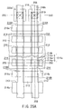
- a third embodiment of the present invention relates to a NAND cell EEPROM.
- FIG. 8 is an equivalent circuit diagram of a NAND cell EEPROM
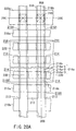
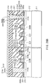
- FIG. 9A is a plan view of a NAND cell EEPROM according to the third embodiment
- FIG. 9B is a sectional view taken along line 9B-9B of FIG. 9A
- FIG. 9C is a sectional view taken along line 9C-9C of FIG. 9A.
- the NAND cell EEPROM has plural NAND cells 40 11 , 40 12 , 40 21 , 40 22 arranged in a matrix on a substrate.
- the plural memory cells MC 1 , ..., MC n in each NAND cell 40 ij are connected in series in such a manner that the adjacent ones of the memory cells share a source/drain region (diffused layer) 9.
- the source line SLj takes the form of diffused layer wires as shown in FIG. 9B (see FIGS. 9A and 9B).
- the gates of the select transistors SDT 11 , SDT 12 are connected to a select line SD 1 and the gates of the select transistors SDT 21 , SDT 22 are connected to a select line SD 2 (see FIG. 8).
- the gates of the select transistors SST 11 , SST 12 are connected to a select line SS 1 and the gates of the select transistors SST 21 , SST 22 are connected to a select line SS 2 (see FIG. 8).
- a barrier insulating film 12 made of silicon nitride has been formed on the element isolating region 4 adjacent to the contact formation region (the diffused layer of the select transistor) in which contacts 42 1 , 42 2 are to be made.
- the barrier insulating film 12 has not been formed on each NAND cell 40 ij , with the gates of the select transistors STD ij , SST ij as a boundary.
- Each NAND cell 40 ij , select transistors STD ij , SST ij , and barrier insulating film 12 are covered with an interlayer insulating film 22.
- an interlayer insulating film 22 On the interlayer insulating film 22, a bit line BL i is formed.
- the bit line BLi is covered with an interlayer film 28.
- the barrier insulating film 12 has been formed on the element isolating region 4 adjacent to the region (the diffused layer of a select transistor) in which contacts 42 1 , 42 2 are to be made. As a result, the contacts 42 1 , 42 2 are prevented from coming into contact with the silicon substrate 2.
- the barrier insulating film 12 has not been formed on each NAND cell 40 ij . Specifically, because the barrier insulating film 12 has not been formed in the vicinity of the gate electrode structure of a memory cell MC k , even if data is written and deleted repeatedly, part of the diffused layer 9 will not turn to a depletion layer. As a result, the drain current (on current) in the memory cell is prevented from reducing, which prevents a decrease in the reliability as much as possible.
- the barrier insulating film 12 has been formed in the vicinity of the gate electrode structure of each of the select transistors SDT ij , SST ij .
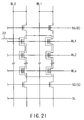
- a fourth embodiment of the present invention relates to an AND cell EEPROM.
- FIG. 10 is an equivalent circuit diagram of an AND cell EEPROM.
- FIG. 11 is a plan view of an AND cell EEPROM according to the fourth embodiment.
- an AND cell EEPROM has plural AND cells 50 arranged in a matrix on a substrate.
- Each AND cell has plural memory cells MC.
- Each memory cell is composed of a transistor having a gate electrode structure (stacked structure) where a gate insulating film, a floating gate, a gate-to-gate insulating film, and a control gate are stacked one on top of another in that order on the substrate.
- One end of each of the plural memory cells in each AND cell 50 is connected to a local source line 56 and the other end of each of them is connected to a local data line 58.
- the select transistor connected to the local data line 58 is connected via a contact hole 52 to the corresponding global data line Di.
- the gate of the select transistor connected to the local source line 56 is connected to a select line ST 1 and the gate of the select transistor connected to the local data line 58 is connected to a select line SD 1 .
- reference symbol 2 indicates a semiconductor substrate and reference symbols 6 1 , ..., 6 n indicate floating gates.
- the barrier insulating film 12 has been formed on the element isolating region 4 adjacent to the region (the diffused layer of a select transistor) in which a contact 52 with the global data line D i is to be formed and on the element isolating region 4 adjacent to the region (the diffused layer of a select transistor) in which a contact 54 with the common source line SL is to be formed. This prevents the contacts 52, 54 from coming into contact with the silicon substrate 2.
- the barrier insulating film 12 has not been formed on each AND cell 50. Specifically, because the barrier insulating film 12 has not been formed in the vicinity of the gate electrode structure of each memory cell MC, even if data is written and deleted repeatedly, part of the diffused layer 9 will not turn to a depletion layer. As a result, the drain current (on current) in the memory cell is prevented from reducing, which prevents a decrease in the reliability as much as possible.
- a fifth embodiment of the present invention relates to a method of manufacturing NAND cell EEPROMs.
- FIGS. 12A to 12G and FIGS. 13A to 13G are sectional views showing manufacturing processes to help explain a method of manufacturing a NAND cell EEPROM according to the fifth embodiment.
- FIGS. 12A to 12G are sectional views corresponding to the sectional view taken along line 9B-9B of FIG. 9A and
- FIGS. 13A to 13G are sectional views corresponding to the sectional view taken along line 9C-9C of FIG. 9A.
- a shallow trench 3 is formed in a region where an element isolating region is to be formed in, for example, a p-type silicon substrate 2. Then, the shallow trench 3 is filled with an element isolation insulating film 4 made of silicon oxide. Following that, a gate insulating film 5, a conductive film 6 to act as a floating gate, an insulating film 7, and a conductive film 8 to act as a control gate are stacked one on top of another in that order on the entire surface of the substrate 2. Patterning these films produces a gate electrode structure.
- silicon oxide is deposited on the p-type silicon substrate by CVD techniques. Then, the insulating film 11 is etched back by RIE techniques, thereby forming a sidewall made of the insulating film 11 on the side of the gate electrode structure. At this time, the insulating film 11 also remains on the gate electrode structure.
- impurity ions are implanted into the element region of the substrate 2, thereby forming a diffused layer 9 for a source and a drain.
- silicon nitride is deposited all over the surface above the substrate 2 using CVD techniques, thereby forming a barrier insulating film 12.
- a resist pattern 14 which is made of photoresist and covers the contact formation region and only the element isolation insulating film 4 adjacent to the region is formed on the barrier insulating film 12. Then, with the resist pattern 14 as a mask, the barrier insulating film 12 is etched using CDE (chemical Dry Etching) techniques.
- CDE chemical Dry Etching
- the diffused layer 9 extends as far as under the sidewall made of the insulating film 11.
- annealing is done to activate the diffused layer 9. At this time, the diffused layer 9 extends as far as under the gate electrode structure.
- an interlayer insulating film 22 is formed all over the surface above the substrate 2. Then, a contact hole 26 is made in the interlayer insulating film 22. Following that, the contact hole is filled with conductive material, thereby forming a contact (not shown) made of the contact material within the contact hole.
- the barrier insulating film 12 is formed only on the contact formation region and the element isolation insulating film 4 adjacent to the region. Specifically, the barrier insulating film 12 has not been formed in the vicinity of the gate electrode structure of each memory cell. Therefore, even if data is written and deleted repeatedly, part of the diffused layer 9 will not turn to a depletion layer. As a result, the drain current (on current) in the transistor is prevented from reducing, which prevents a decrease in the reliability as much as possible.
- the contact 26 will not penetrate to the substrate 2.
- the diffused layer 9 for the source and drain is less liable to extend as far as under the gate electrode structure, even when annealing is done to improve the quality of the sidewall made of the insulating film 11 and another annealing is done to activate the diffused layer. As a result, the short channel effect in the transistor can be suppressed.
- a sixth embodiment of the present invention relates to a method of manufacturing NAND cell EEPROMs.
- FIGS. 14A to 14G and FIGS. 15A to 15G are sectional views showing manufacturing processes to help explain a method of manufacturing a NAND cell EEPROM according to the sixth embodiment.
- FIGS. 14A to 14G are sectional views corresponding to the sectional view taken along line 9B-9B of FIG. 9A and
- FIGS. 15A to 15G are sectional views corresponding to the sectional view taken along line 9C-9C of FIG. 9A.
- a shallow trench 3 is formed in a region where an element isolating region is to be formed in, for example, a p-type silicon substrate 2. Then, the shallow trench 3 is filled with an element isolation insulating film 4 made of silicon oxide. Following that, a gate insulating film 5, a conductive film 6 to act as a floating gate, an insulating film 7, and a conductive film 8 to act as a control gate are stacked one on top of another in that order on the entire surface of the substrate 2. Patterning these films produces a gate electrode structure. Next, using CVD techniques, for example, silicon oxide is deposited only on the element region of the p-type silicon substrate 2, thereby forming an insulating film 11. Then, the insulating film 11 is etched back by RIE techniques, thereby forming a sidewall made of the insulating film 11 on the side of the gate electrode structure. At this time, the insulating film 11 also remains on the gate electrode structure.
- impurity ions are implanted into the element region of the substrate 2, thereby forming a diffused layer 9 for a source and a drain.
- silicon nitride is deposited all over the surface above the substrate using CVD techniques, thereby forming a barrier insulating film 12.
- the barrier insulating film 12 for example, silicon oxide is deposited using CVD techniques, thereby forming an insulating film 13.
- a resist pattern 18 which is made of photoresist and covers only the contact formation region and the element isolation insulating film 4 adjacent to the region is formed on the insulating film 13. Then, with the resist pattern 18 as a mask, the insulating film 13 is etched using wet etching techniques.
- the barrier insulating film 12 is etched with the insulating film 13 as a mask, using wet etching with the selectivity of the insulating film 13 to the barrier insulating film 12.
- annealing is done to activate the diffused layer 9. At this time, the diffused layer 9 extends as far as under the gate electrode structure.
- the manufacturing method of the sixth embodiment produces a similar effect to that of the manufacturing method of the fifth embodiment.
- a seventh embodiment of the present invention relates to a NAND cell EEPROM with a booster plate.
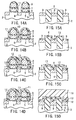
- FIGS. 16A to 16D schematically show the configuration of a memory cell array in a conventional NAND EEPROM.
- FIG. 16A is a plan view showing the internal structure
- FIG. 16B is a sectional view taken along line 16B-16B of FIG. 16A
- FIG. 16C is a sectional view taken along line 16C-16C of FIG. 16A
- FIG. 16D is a sectional view taken along line 16D-16D of FIG. 16A.
- a well region 102 is provided at the main surface of a semiconductor substrate 101.
- STI-structure element isolating regions 103 are formed in such a manner that part of the element isolating regions 103 are selectively projected above the main surface of the semiconductor substrate 101.
- MOS transistors memory cells 104 of a stacked gate structure are arranged in a matrix.
- Each of the memory cells 104 is composed of a gate electrode section 104a selectively provided on a thin oxide film (tunnel oxide film) 105 at the surface of the well region 102 and a diffused layer region 104b that is to act as a drain or a source and provided at the surface of the well region 102 corresponding to the space between the gate electrode sections 104a.
- Each diffused layer region 104b is shared by other memory cells 104 adjacent to each other in the direction of column line, for example, bit line (BL).
- Plural memory cells are connected in series, thereby forming a single NAND cell (memory cell unit).
- Each of the gate electrode sections 104a is composed of a structure where a floating gate 104a-1 acting as a charge storage layer, a gate-to-gate insulating film 104a-2, and a control gate 104a-3 stacked in that order on the channel region between the diffused layer regions 104b.
- the control gate 104a-3 is shared by, for example, other gate electrode section 104a in the direction of row line and functions as a word line (WL).
- Select gate (SG) transistors (a drain-side select gate 106A and a source-side select gate 106B) are provided at, for example, both ends of the NAND cell in the direction of bit line.
- the drain-side select gate 106A is composed of a gate electrode 106a provided on the tunnel oxide film 105 and a diffused layer region 106b adjacent to the gate electrode 106a, provided at the surface of the well region 102, and acting as a drain.
- a diffused layer region acting as a source is shared by the memory cells 104 at the ends adjacent to the drain-side select gate 106A.
- the source-side select gate 106B is composed of a gate electrode 106a provided on the tunnel oxide film 105 and a diffused layer region 106b adjacent to the gate electrode 106a, provided at the surface of the well region 102 so as to be shared by other source-side select gates 106B adjacent to each other in the direction of row line, and acting as a source line (SL).
- a diffused layer region acting as a drain is shared by the memory cells 104 at the ends adjacent to the source-side select gate 106B.
- each gate electrode 106a has a structure where a second gate 106a-3 made of the same material as that of the control gate 104a-3 is stacked on a first gate 106a-1 made of the same material as that of the floating gate 104a-1.
- Each gate electrode 106a is shared by, for example, other select gates 106A and 106B in the direction of row line.
- an interlayer insulating film 107 is provided on the main surface of the semiconductor substrate 101 in such a manner that the memory cells 104 and select gates 106A and 106B are covered with the interlayer insulating film 107.
- bit lines 108 are provided in the direction of the column of the memory cells 104. Each bit line 108 is connected to the diffused layer region 106b of the drain-side select gate 106A by a bit-line contact 109 provided so as to penetrate through the interlayer insulating film 107 and tunnel oxide film 105.
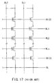
- FIG. 17 is an equivalent circuit diagram of a memory cell array of the above-described structure.
- Data is written into, erased from, and read from the memory cell array by making use of an exchange of electrons between the floating gate 104a-1 and well region 102 under the potential relationship shown in Program Erase Read BL1 (selected) 0 floating 1V BL2 (unselected) Vcc floating 0 SG (D) Vcc floating Vread WL2 (selected) Vppw 0 0 WL1, 3 ... n (unselected) Vpass floating Vread SG (S) 0 floating Vread SL 0 floating 0 Well 0 Vppe 0
- Vppw e.g. 20V
- 0V 0V
- passing current into the tunnel oxide film causes electrons to be injected from the well region into the floating gate by a tunnel phenomenon.
- the threshold voltage of the transistor in the memory cell goes positive, thereby writing the data.
- the data is written simultaneously into all the transistors (memory cells) connected to the selected control gate.
- 0V is applied to the bit line to which the selected cell (the memory cell into which the data is to be written) is connected and Vcc (e.g., 3V) is applied to the bit line to which the unselected cells (the memory cells into which the data is not written) are connected.
- Vcc e.g., 3V
- Vcc is applied to the select gate on the drain side and a potential of Vpass (e.g., 10V) is applied to the control gates of the unselected cells so that 0V is transferred to the selected cell.
- Vpass e.g. 10V
- Vppw (e.g., 20V) is applied to the control gates. Then, in the selected cell, Vppw is applied to the control gate and 0V is applied to the well region, thereby selectively writing the data.
- drain-side select gates of the unselected cells are cut off, because Vcc is applied to the bit line.
- the source-side select gates are also cut off, because 0V is applied to the source lines and to the gates. As a result, all the memory cells connected to the bit line go into the floating state.
- Vppe e.g. 20V
- erasing is generally done in such a manner that all of the selected block is erased from.
- Reading is done by making use of the positive and negative threshold voltages of the transistor in the memory cell. For example, 1V is applied to the selected bit line and 0V is applied to the selected control gate, and the data is judged, depending on whether current flows in the transistor or not. At this time, a read potential of Vread (e.g., 5V) is applied so that all of the control gates and select gates of the unselected cells may turn on.
- Vread e.g., 5V
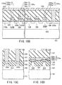
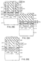
- FIGS. 18A to 18D schematically show the configuration of a conventional memory cell array with a booster plate in a NAND EEPROM.
- FIG. 18A is a plan view showing the internal structure
- FIG. 18B is a sectional view taken along line 18B-18B of FIG. 18A
- FIG. 18C is a sectional view taken along line 18C-18C of FIG. 18A
- FIG. 18D is a sectional view taken along line 18A-18A of FIG. 18A.
- a booster plate 112 made of conductive material is provided so as to cover the gate electrode section 104a of the memory cell 104 via a plate insulating film 111.
- the high voltage Vppw is also applied to the booster plate 112, thereby increasing the substantial capacitive coupling ratio, which not only enables the channel potential at the unselected cells in a write operation to rise sufficiently, but also makes the high voltage Vppw (about 14V) applied to the control gate lower than when the booster plate 112 is not used.
- the interlayer insulating film 107 and the plate insulating film 111 and tunnel oxide film 105 under the interlayer insulating film 107 are removed consecutively by reactive ion etching or the like, thereby making the contact hole 109a leading to the diffused layer region 106b of the drain-side select gate 106A, as shown in FIGS. 19A and 19B.
- the reactive ion etching is controlled in such a manner that the etching is stopped when the diffused layer region 106b is exposed.
- Etching to make the contact hole 109a is generally done somewhat excessively. The reason for this is to absorb variations in the processes, including the film thickness of the interlayer insulating film 107 and the etching speed. Even in the worst case, etching has to be effected until the surface of the element region has certainly been exposed.
- the element isolating region 103 is etched at the same time.
- the etching speed and the thickness of the interlayer insulating film 107 vary in the same wafer or from one wafer to another in terms of processes, it is actually difficult to stop etching suitably at the time when the element region has been exposed and there is a strong possibility that the element isolating region 103 will also be etched. If the contact hole 109a has reached the bottom surface of the element isolating region 103, the effective distance between adjacent bit line contacts 109 becomes shorter, permitting punch-through to occur between bit lines, which contributes to faulty operations.
- LOC selective oxidation
- the diameter of the contact hole 109a were made smaller to prevent the element isolating region 103 from being etched, it would be difficult to effect patterning in the photolithographic process or the aspect ratio of the contact hole 109a would increase, making the etching and the embedding of conductive material difficult. Conversely, if the width of the element region were increased, the area of the memory cell array would increase. This is undesirable.
- the object of the seventh embodiment is to provide a nonvolatile semiconductor memory device capable of preventing a faulty operation resulting from the accuracy of work in making a contact hole and improving the characteristic and reliability of the device and a method of manufacturing the nonvolatile semiconductor memory device.
- FIGS. 20A to 20D schematically show the configuration of a nonvolatile semiconductor memory according to the seventh embodiment in, for example, a memory cell array of a NAND EEPROM.
- FIG. 20A is a plan view showing the internal structure
- FIG. 20B is a sectional view taken along line 20B-20B of FIG. 20A
- FIG. 20C is a sectional view taken along line 20C-20C of FIG. 20A
- FIG. 20D is a sectional view taken along line 20D-20D of FIG. 20A.
- a well region 212 is provided at the main surface of a semiconductor substrate 211.
- STI-structure element isolating regions (element isolation insulating films) 213 are formed in such a manner that part of the element isolating regions 103 are selectively projected above the main surface of the semiconductor substrate 211.
- MOS transistors (memory cells 214) of a stacked gate structure are arranged in a matrix.
- Each of the memory cells 214 is composed of a gate electrode section 214a selectively provided on a thin tunnel oxide film (gate insulating film) 215 at the surface of the well region 212 and a diffused layer region 214b that acts as a drain or a source and is provided at the surface of the well region 212 corresponding to the space between the gate electrode sections 214a.
- a thin tunnel oxide film gate insulating film
- the tunnel oxide film 215 is composed of about 10-nm-thick silicon oxide film, silicon nitride film, or silicon oxynitride film, or a stacked film of those films.
- Each of the diffused layer regions 214b is formed by ion-implanting or thermally diffusing impurities of the opposite conductivity to that of the well region 212.
- Each diffused layer region 214b is shared by other memory cells 214 adjacent to each other in the direction of column line, for example, bit line (BL).
- Each of the gate electrode sections 214a is composed of a structure where a floating gate 214a-1 acting as a charge storage layer, a gate-to-gate insulating film 214a-2, and a control gate 214a-3 stacked in that order on the channel region between the diffused layer regions 214b.
- the floating gate 214a-1 which is made of, for example, polycrystalline silicon or amorphous silicon, is electrically isolated from the surrounding conductive layer by the tunnel oxide film 215 and gate-to-gate insulating film 214a-2.
- the gate-to-gate insulating film 214a-2 is composed of a silicon oxide film, a silicon nitride film, or a silicon oxynitride film, or a stacked film of those films.
- the control gate 214a-3 which is provided so as to cross the element region, is shared by, for example, other gate electrode sections 214a in the direction of row line and functions as a word line (WL).
- plural (for example, 16) memory cells 14 are connected in series in the direction of bit line, thereby forming a NAND cell serving as a memory cell unit.
- select gate (SG) transistors a drain-side select gate (SG(D)) 216A and a source-side select gate (SG(SS)) 216B are provided.
- Each drain-side select gate 216A is composed of a gate electrode 216a provided on the tunnel oxide film 215 and a diffused layer region 216b adjacent to the gate electrode 216a, provided at the surface of the well region 212, and acting as a drain.
- a diffused layer region acting as a source is shared by the memory cells 214 at the ends adjacent to the drain-side select gate 216A.
- Each source-side select gate 216B is composed of a gate electrode 216a provided on the tunnel oxide film 215 and a diffused layer region 216b adjacent to the gate electrode 216a, provided at the surface of the well region 212 so as to be shared by other source-side select gates 216B adjacent to each other in the direction of row line, and acting as a source line (SL).
- a diffused layer region acting as a drain is shared by the memory cells 214 at the ends adjacent to the source-side select gate 216B.
- each gate electrode 216a has a structure where a second gate 216a-3 made of the same material as that of the control gate 214a-3 is stacked on a first gate 216a-1 made of the same material as that of the floating gate 214a-1.
- Each gate electrode 216a which is provided so as to cross the element region, is shared by, for example, other select gates 216A and 216B in the direction of row line.
- a booster plate 222 is provided on the main surface of the semiconductor substrate 211 in such a manner that at least part of the gate electrode section 214a of each memory cell 204 is covered with the booster plate 222 via the plate insulating film 221.
- the plate insulating film 221, which is provided so as to cover at least the main surface of the semiconductor substrate 211, is composed of, for example, a silicon oxide film, a silicon nitride film, or a silicon oxynitride film, or a stacked film of those films.
- the booster plate 222 is composed of a polycrystalline silicon film (or a conductive layer of tungsten polycide or the like) whose resistance has been made lower by doping a lot of impurities. In addition to covering all of the memory cell 214 excluding the select gates 216A, 216B, the booster plate 222 may be provided so as to cover only part of the memory cell 214.
- An etching stop layer (cover layer) 222a is provided integrally on the top surface of each diffused layer region 216b of the drain-side select gate 216A via the tunnel oxide film 215 and plate insulating film 221.
- the etching stop layer 222a is formed out of the polycrystalline silicon film whose resistance has been made lower by doping a lot of impurities and which constitutes the booster plate 222.
- an interlayer insulating film 217 is provided on the main surface of the semiconductor substrate 211 in such a manner that the memory cell 214 and select gates 216A, 216B are covered with the interlayer insulating film 217.
- bit lines 218 are arranged in the direction of column of the memory cells 214. Each bit line 218 is connected to the diffused layer region 216b of the drain-side select gate 216A by a bit line contact (contact section) 219.
- Each bit line contact 219 is formed by filling a contact hole 219a with conductive filler (or conductive material) 219b.
- the contact hole 219a is made so as to penetrate through, for example, the interlayer insulating film 217, etching stop layer 222a, plate insulating film 221, and tunnel oxide film 215.
- Each bit line contact 219 is electrically insulated in such a manner that a sidewall insulating film 219c is formed on the inner wall face of the contact hole 219a in contact with the etching stop layer 222a to prevent the bit line contacts 219 from being short-circuited to each other via the etching stop layer 22a.
- the sidewall insulating film 219c is formed out of, for example, a silicon oxide film or a silicon nitride film. Polycrystalline silicon, amorphous silicon, or tungsten is used for the filler 219b.
- the memory cell array operates similarly to a conventional memory cell array with a booster plate.
- FIG. 21 is an equivalent circuit diagram of a memory cell array of the above-described structure.
- Data is written into, erased from, and read from the memory cell array by making use of an exchange of electrons between the floating gate 214a-1 and well region 212 under the potential relationship shown in Program Erase Read BL1 (selected) 0 floating 1V BL2 (unselected) Vcc floating 0 SG (D) Vcc floating Vcc Booster Plate Vppw 0 Vcc WL2 (selected) Vppw 0 0 WL1, 3 ... n (unselected) Vcc floating Vcc SG (S) 0 floating Vcc SL 0 floating 0 Well 0 Vppe 0
- Vppw e.g., 214V
- booster plate 222 0V is applied to the diffused layer region (drain/source) 214b and well region 212.
- the booster plate 222 provided on the sidewall of the floating gate 214a-1 increases the substantial coupling ratio, which enables the voltage Vppw applied to the control gate 214a-3 to be lower than when the booster plate is not used.
- Vppe voltage Vppe applied to the control gate 214a-3 can be made lower than when the booster plate is not used.
- Vcc e.g., 3V
- FIGS. 22A to 22G correspond to the cross section taken along line 20B-20B of FIG. 20A.
- FIGS. 23A to 23G correspond to the cross section taken along line 20C-20C of FIG. 20A.
- FIGS. 24A to 24G correspond to the cross section taken along line 20D-20D of FIG. 20A.
- the gate electrode section 214a of the memory cell 214 and the gate electrodes 216a of the drain-side select gate 216A and source-side select gate 216B are formed similarly to the existing NAND EEPROM.
- an oxidation process may be carried out to form a gate sidewall oxide film of about 100 angstroms in thickness.
- impurities are introduced into the main surface of the semiconductor substrate 211 by ion implantation, thereby forming diffused layer regions 214b, 216b.
- a silicon oxide film of about 500 angstroms in thickness is deposited all over the surface above the semiconductor substrate 311 by, for example, CVD (Chemical Vapor Deposition) techniques, thereby forming a plate insulating film 21.
- a polycrystalline silicon film 222' to form a booster plate 222 is deposited on the plate insulating film 221 by CVD techniques.
- the polycrystalline silicon film 222' is patterned by a photolithographic method, thereby etching away part of the silicon film 222'.
- the booster plate 222 is formed so as to cover the gate electrode sections 214a of at least part of the memory cells 214 and an etching stop layer 222a is formed on the top surface of each diffused layer region 216b of the drain-side select gate 216A.
- an interlayer insulating film 217 of about 10000 angstroms in thickness is deposited all over the surface above the semiconductor substrate 211.
- a contact hole (first opening) 219a-1 reaching the etching stop layer 222a is made by a photolithographic method to form a bit line contact 219 in the interlayer insulating film 217.
- the interlayer insulating film 217 is etched, it is relatively easy to give selectivity to the polycrystalline silicon film 222', which stops the etching surely at the time when the etching stop layer is exposed. As a result, it is possible to prevent the element isolating region 213 and the like from being etched more than is necessary.
- the etching stop layer 22a exposed at the bottom of the contact hole 219a-1 is etched away, thereby making a contact hole (second opening) reaching the underlying plate insulating film 221.
- the etching stop layer 22a is etched, it is relatively easy to give selectivity to the plate insulating film 221, which stops the etching surely at the time when the etching stop layer is exposed, even if etching is done somewhat excessively.
- the plate insulating film 221 and tunnel oxide film 215 are etched away, thereby making a contact hole (third opening).
- a sidewall insulating film 219c is formed in the contact hole 219a.
- the sidewall insulating film 219c is formed in such a manner that a silicon oxide film is deposited all over the surface and then anisotropic etching is effected to leave the silicon oxide film only on the inner wall face of the contact hole 219a.
- the filler 219b is embedded in the contact hole 219a and the bit line 218 is patterned, thereby completing a NAND EEPROM memory cell array of the structure shown in FIGS. 20A to 20D.
- the etching of the interlayer insulating film in making the contact hole to form a bit line contact can be stopped temporarily at the time when the etching stop layer is exposed.
- a conductive layer which is used as a booster plate, is formed so as to cover the gate electrode section of the memory cell.
- the conductive layer is also formed on the bottom of the bit line contact. This enables the conductive layer to be used as an etching stopper in making a contact hole. As a result, not only are the characteristics of the device improved, but also the contact hole is prevented from being etched excessively. Because the element isolating region is prevented from being etched more than is necessary, not only are the characteristics of the device improved, but also faulty operations stemming from the processes in making a contact hole, such as the occurrence of punch-through between bit lines, can be eliminated.
- the etching stop layer is formed simultaneously with the booster plate, there is no fear that the manufacturing processes become complex.
- the etching stop layer 222a has been formed in a stripe in such a manner that it is provided integrally on the top surface of each diffused layer region 216b of the drain-side select gate 216A so as to be shared by the regions 216b.
- the present invention is not limited to this.
- the etching stop layer 222a may be provided independently on the top surface of each diffused layer region 216b of the drain-side select gate 216A.
- the etching of the interlayer insulating film in making a contact hole to form a contact section can be stopped temporarily at the time when the cover layer is exposed. This prevents the element isolation insulating film from being etched than is necessary.
- An eighth embodiment of the present invention relates to a NAND cell EEPROM with a booster plate.
- FIGS. 25A to 25D schematically show the configuration of a nonvolatile semiconductor memory according to the eighth embodiment in, for example, a memory cell array of a NAND EEPROM.
- FIG. 25A is a plan view showing the internal structure
- FIG. 25B is a sectional view taken along line 25B-25B of FIG. 25A
- FIG. 25C is a sectional view taken along line 25C-25C of FIG. 25A
- FIG. 25D is a sectional view taken along line 25D-25D of FIG. 25A.
- etching stop layers 222a' are provided independently to adjacent bit line contacts 219 in such a manner that the layers 222a' are separated from each other. In this case, because there is no need to electrically insulate the bit line contacts 219 from each other to prevent them from short-circuiting with each other via the etching stop layers 222a', the formation of the sidewall insulating film 219c can be omitted.
- the eighth embodiment not only produces almost the same effect as that of the seventh embodiment, but also enables remarkable simplification in terms of structure and manufacturing process.
- the etching stop layer does not necessarily need to be formed at the same time when the booster plate 222 is formed. For instance, it may be formed at the same time when the source wires connected to the diffused layer regions (source lines) 216b of the source-side select gate 216B are formed.
- a ninth embodiment of the present invention relates to a NAND cell EEPROM with source wires connected to diffused layer regions 216b.
- FIGS. 26A to 26E schematically show the configuration of a nonvolatile semiconductor memory according to the ninth embodiment in, for example, a memory cell array of a NAND EEPROM.
- FIG. 26A is a plan view showing the internal structure
- FIG. 26B is a sectional view taken along line 26B-26B of FIG. 26A
- FIG. 26C is a sectional view taken along line 26C-26C of FIG. 26A
- FIG. 26D is a sectional view taken along line 26D-26D of FIG. 26A
- FIG. 26E is a sectional view taken along line 26E-26E of FIG. 26A.
- a conductive layer 222b to act as source wires is provided on the main surface of the semiconductor substrate 211 via the tunnel oxide film 215 and an insulating film 221' in such a manner that the conductive layer 222b covers common source regions (or each diffused layer region 216b of the source-side select gate 216B).
- the conductive layer 222b is locally connected to the diffused layer region 216b via a source contact 219'. In this case, the conductive layer 222b is electrically short-circuited to the source contact 219', thereby functioning as a source wire.
- the insulating film 221' which is provided so as to cover at least the main surface of the semiconductor substrate 211, is made of a silicon oxide film, a silicon nitride film, or a silicon oxynitride film, or a stacked film of those films.
- the conductive layer 222b is composed of a polycrystalline silicon film (or tungsten polycide or the like) whose resistance has been made lower by doping a lot of impurities.
- the source contact 219' is formed by filling a contact hole 219a' with conductive filler (or conductive material) 219b'.
- the contact hole 219a' is made so as to penetrate, for example, the interlayer insulating film 217, conductive layer 222b, insulating film 221', and tunnel oxide film 215.
- an etching stop layer (cover layer) 222a is provided integrally on the top surface of each diffused layer region 216b of the drain-side select gate 216A via the tunnel oxide film 215 and insulating film 221'.
- the etching stop layer 222a is formed out of the polycrystalline silicon film whose resistance has been made lower by doping a lot of impurities and which constitutes the conductive layer 222b.
- the bit line contact 219 penetrates through the interlayer insulating film 217, etching stop layer 222a, insulating film 221', and tunnel oxide film 215 and is connected to each diffused layer region 126b of the drain-side select gate 216A.
- Each bit line contact 219 is connected to the bit line 218 via a separate contact via 224 provided in the interlayer insulating film 223.
- the interlayer insulating film 223 is formed to an almost uniform thickness on the entire surface of the interlayer insulating film 217, including, for example, the source contact 219' and the top surface of the bit line contact 219.
- the contact via 224 is formed by filling a via hole 224a with conductive filler (or conductive material) 224b.
- the via hole 224a is made so as to penetrate through the interlayer insulating film 223.
- bit line contacts 219 are electrically insulated from each other in such a manner that a sidewall insulating film 219c is formed on the inner wall face of the contact hole 219a in contact with the etching stop layer 222a to prevent the bit line contacts 219 from being short-circuited to each other via the etching stop layer 222a.
- FIGS. 27A to 27D a method of manufacturing a memory cell array constructed as described above will be explained.
- FIGS. 27A to 27D correspond to the cross section taken along line 26B-26B of FIG. 26A.
- FIGS. 28A to 28D correspond to the cross section taken along line 26C-26C of FIG. 26A.
- FIGS. 29A to 29D correspond to the cross section taken along line 26D-26D of FIG. 26A.
- the polycrystalline silicon film 222' is patterned by a photolithographic method, thereby etching away part of the silicon film 222'.
- a conductive layer 222b to act as source wires is formed so as to cover each diffused layer region 216b of the source-side select gate 216B.
- an etching stop layer 222a is formed on the top surface of each diffused layer region 216b of the drain-side select gate 216A.
- an interlayer insulating film 217 is deposited to a thickness of about 10000 angstroms all over the surface.
- a contact hole (first opening) 219a-1 reaching the etching stop layer 222a is made by a photolithographic method to form a bit line contact 219 in the interlayer insulating film 217.
- a contact hole (first opening) 219a-1' reaching the conductive layer 222b is made to form a bit line contact 219'.
- the etching stop layer 222a exposed at the bottom of the contact hole 219a-1 and the conductive layer 222b exposed at the bottom of the contact hole 219a-1' are etched away and a contact hole (second opening) reaching the underlying insulating film 221' is made.
- the insulating film 221' and tunnel oxide film 15 are etched away and a contact hole (third opening) is made.
- contact holes 219a, 219a' reaching the diffused layer 216b are finally made as shown in FIGS. 27C, 28C, and 29C.
- the element isolating region 213, which should not have been etched, has been etched.
- the insulating film 221' and tunnel oxide film 215 are thin. Therefore, the absolute amount of excess etching is smaller than the amount of excess etching when the interlayer insulating film 217 is etched. As a result, the amount by which the element isolating region 213 is etched can be reduced.
- a sidewall insulating film 219c is formed only in the contact hole 219a.
- the sidewall insulating film 219c is formed in such a manner that a silicon oxide film is deposited all over the surface and then anisotropic etching is effected to leave the silicon oxide film only on the inner wall face of the contact holes 219a, 219a'. Then, only the silicon oxide film remaining on the inner wall face of the contact hole 219a' is selectively removed.
- an interlayer insulating film 223 is deposited all over the surface. Then, a via hole 224a reaching the bit line contact 219 is made in the interlayer insulating film 223.
- the conductive layer 222b has been provided on the diffused layer region 216b of the source-side select gate 216B and is used as a source wire.
- another conductive layer (etching stop layer 222a) has been formed at the bottom of the bit line contact 219. This enables the conductive layers to act as etching stoppers in making the contact hole 219a.
- the contact hole 219a is prevented from being etched excessively. This not only prevents the element isolating region 213 and others from being etched more than is necessary, but also decreases the resistance of the source line (source-side select gate 216B). Consequently, the reliability of the memory cell 214 is improved (because faulty operations are prevented) and the area of the memory cell array is decreased as a result of a reduction in the number of common source lines connected to the individual source lines. Therefore, an improvement in the characteristics of the device and an improvement in the controllability in manufacturing processes can be realized at the same time.
- the etching stop layer 222a may be provided independently on the top surface of each diffused layer region 216b of the drain-side select gate 216A.
- a tenth embodiment of the present invention relates to a NAND cell EEPROM with source wires connected to diffused layer regions 216b.
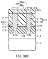
- FIGS. 30A to 30C schematically show the configuration of a nonvolatile semiconductor memory according to the tenth embodiment in, for example, a memory cell array of a NAND EEPROM.
- FIG. 30A is a plan view showing the internal structure
- FIG. 30B is a sectional view taken along line 30B-30B of FIG. 30A
- FIG. 30C is a sectional view taken along line 30C-30C of FIG. 30A.
- etching stop layers 222a' are provided independently to adjacent bit line contacts 219 in such a manner that they are separated from each other. In this case, because there is no need to electrically insulate the bit line contacts 219 from each other to prevent them from short-circuiting with each other via the etching stop layers 222a', the formation of the sidewall insulating film 219c can be omitted.
- the tenth embodiment enables remarkable simplification in terms of structure and manufacturing process.
- the diffused layer region 216b of the source-side select gate 216b does not necessarily need to be formed as a common source region shared by the adjacent source-side select gates 216B in the direction of row line.
- the diffused layer regions 216b may be provided separately by causing the element isolating region 213 to extend between the diffused layer regions 216b of the adjacent source-side select gates 216B.
- an etching stop layer may be formed on the diffused layer region of the drain-side select gate at the same time when a booster plate and source wires are formed.
- nonvolatile semiconductor memory device capable of preventing faulty operations owing to the accuracy of work in making a contact hole and improving the characteristics and the reliability of the device.
Landscapes
- Semiconductor Memories (AREA)
- Non-Volatile Memory (AREA)
Applications Claiming Priority (4)
| Application Number | Priority Date | Filing Date | Title |
|---|---|---|---|
| JP10370757A JP2000196046A (ja) | 1998-12-25 | 1998-12-25 | 不揮発性半導体記憶装置およびその製造方法 |
| JP37075798 | 1998-12-25 | ||
| JP30372699 | 1999-10-26 | ||
| JP30372699A JP2001127273A (ja) | 1999-10-26 | 1999-10-26 | 半導体装置およびその製造方法 |
Publications (2)
| Publication Number | Publication Date |
|---|---|
| EP1014448A2 true EP1014448A2 (de) | 2000-06-28 |
| EP1014448A3 EP1014448A3 (de) | 2000-10-11 |
Family
ID=26563605
Family Applications (1)
| Application Number | Title | Priority Date | Filing Date |
|---|---|---|---|
| EP99125534A Withdrawn EP1014448A3 (de) | 1998-12-25 | 1999-12-22 | Nichtflüchtiges Halbleiterspeicherbauelement und dessen Herstellungsverfahren |
Country Status (3)
| Country | Link |
|---|---|
| EP (1) | EP1014448A3 (de) |
| KR (2) | KR100360183B1 (de) |
| TW (1) | TW517375B (de) |
Cited By (2)
| Publication number | Priority date | Publication date | Assignee | Title |
|---|---|---|---|---|
| WO2005124864A1 (en) * | 2004-06-15 | 2005-12-29 | Koninklijke Philips Electronics N.V. | 2-transistor memory cell with modified access gate |
| US7723776B2 (en) | 2005-10-04 | 2010-05-25 | Samsung Electronics Co., Ltd. | Flash memory devices having shared sub active regions |
Families Citing this family (2)
| Publication number | Priority date | Publication date | Assignee | Title |
|---|---|---|---|---|
| JP5792918B2 (ja) * | 2000-08-14 | 2015-10-14 | サンディスク・スリー・ディ・リミテッド・ライアビリティ・カンパニーSandisk 3D Llc | 高集積メモリデバイス |
| KR101040495B1 (ko) * | 2009-06-04 | 2011-06-09 | 이양규 | 에지밴딩기의 상하 스크래핑장치 |
Family Cites Families (4)
| Publication number | Priority date | Publication date | Assignee | Title |
|---|---|---|---|---|
| US4982250A (en) * | 1989-01-04 | 1991-01-01 | Motorola, Inc. | Mosture barrier for floating gate transistors |
| JPH07123146B2 (ja) * | 1990-07-05 | 1995-12-25 | 株式会社東芝 | 不揮発性半導体記憶装置の製造方法 |
| JPH0595044A (ja) * | 1991-10-01 | 1993-04-16 | Hitachi Ltd | 半導体装置およびその製造方法 |
| JP3483090B2 (ja) * | 1996-06-19 | 2004-01-06 | ソニー株式会社 | 半導体装置の製造方法 |
-
1999
- 1999-12-22 EP EP99125534A patent/EP1014448A3/de not_active Withdrawn
- 1999-12-24 TW TW088122934A patent/TW517375B/zh active
- 1999-12-27 KR KR1019990062553A patent/KR100360183B1/ko not_active Expired - Fee Related
-
2002
- 2002-03-26 KR KR1020020016488A patent/KR100352756B1/ko not_active Expired - Fee Related
Cited By (4)
| Publication number | Priority date | Publication date | Assignee | Title |
|---|---|---|---|---|
| WO2005124864A1 (en) * | 2004-06-15 | 2005-12-29 | Koninklijke Philips Electronics N.V. | 2-transistor memory cell with modified access gate |
| US7723776B2 (en) | 2005-10-04 | 2010-05-25 | Samsung Electronics Co., Ltd. | Flash memory devices having shared sub active regions |
| US8021978B2 (en) | 2005-10-04 | 2011-09-20 | Samsung Electronics Co., Ltd. | Methods of fabricating flash memory devices having shared sub active regions |
| US8329574B2 (en) | 2005-10-04 | 2012-12-11 | Samsung Electronics Co., Ltd. | Methods of fabricating flash memory devices having shared sub active regions |
Also Published As
| Publication number | Publication date |
|---|---|
| KR100352756B1 (ko) | 2002-09-16 |
| TW517375B (en) | 2003-01-11 |
| KR20000048420A (ko) | 2000-07-25 |
| KR100360183B1 (ko) | 2002-11-08 |
| KR20020029035A (ko) | 2002-04-17 |
| EP1014448A3 (de) | 2000-10-11 |
Similar Documents
| Publication | Publication Date | Title |
|---|---|---|
| JP3966707B2 (ja) | 半導体装置及びその製造方法 | |
| US7696559B2 (en) | Semiconductor memory device including pillar-shaped semiconductor layers and a method of fabricating the same | |
| JP4102112B2 (ja) | 半導体装置及びその製造方法 | |
| US6531732B2 (en) | Nonvolatile semiconductor memory device, process of manufacturing the same and method of operating the same | |
| US6512262B2 (en) | Non-volatile semiconductor memory device and method of manufacturing the same | |
| JP4282248B2 (ja) | 半導体記憶装置 | |
| JP4330670B2 (ja) | 不揮発性半導体記憶装置 | |
| US20100044773A1 (en) | Semiconductor memory device | |
| US8604517B2 (en) | Non-volatile semiconductor memory device for suppressing deterioration in junction breakdown voltage and surface breakdown voltage of transistor | |
| KR101398666B1 (ko) | 플래시 메모리 장치 및 이의 구동 방법 | |
| US7636256B2 (en) | Semiconductor memory device | |
| US20080006885A1 (en) | Semiconductor integrated circuit device and method of manufacturing | |
| US20090091040A1 (en) | Semiconductor device and semiconductor storage device | |
| CN100517723C (zh) | 非易失性半导体存储器件 | |
| JPH11195718A (ja) | 不揮発性半導体記憶装置と、その製造方法及びその駆動方法 | |
| JP2007142468A (ja) | 半導体装置 | |
| JP4970402B2 (ja) | 半導体記憶装置 | |
| EP1014448A2 (de) | Nichtflüchtiges Halbleiterspeicherbauelement und dessen Herstellungsverfahren | |
| US20100001401A1 (en) | Semiconductor device including interconnect layer made of copper | |
| JP7520928B2 (ja) | フラッシュメモリ | |
| JP2006310564A (ja) | 不揮発性半導体記憶装置およびその製造方法 | |
| JPH118367A (ja) | 不揮発性半導体記憶装置及びその製造方法 | |
| CN118510280A (zh) | 具有高集成化的快闪存储器 |
Legal Events
| Date | Code | Title | Description |
|---|---|---|---|
| PUAI | Public reference made under article 153(3) epc to a published international application that has entered the european phase |
Free format text: ORIGINAL CODE: 0009012 |
|
| 17P | Request for examination filed |
Effective date: 19991222 |
|
| AK | Designated contracting states |
Kind code of ref document: A2 Designated state(s): DE FR GB |
|
| AX | Request for extension of the european patent |
Free format text: AL;LT;LV;MK;RO;SI |
|
| PUAL | Search report despatched |
Free format text: ORIGINAL CODE: 0009013 |
|
| AK | Designated contracting states |
Kind code of ref document: A3 Designated state(s): AT BE CH CY DE DK ES FI FR GB GR IE IT LI LU MC NL PT SE |
|
| AX | Request for extension of the european patent |
Free format text: AL;LT;LV;MK;RO;SI |
|
| AKX | Designation fees paid |
Free format text: DE FR GB |
|
| STAA | Information on the status of an ep patent application or granted ep patent |
Free format text: STATUS: THE APPLICATION HAS BEEN WITHDRAWN |
|
| 18W | Application withdrawn |
Effective date: 20030218 |