EP1014458A2 - Procédés de fabrication d'une matrice d'affichage électroluminescente organique en couleur - Google Patents
Procédés de fabrication d'une matrice d'affichage électroluminescente organique en couleur Download PDFInfo
- Publication number
- EP1014458A2 EP1014458A2 EP99204212A EP99204212A EP1014458A2 EP 1014458 A2 EP1014458 A2 EP 1014458A2 EP 99204212 A EP99204212 A EP 99204212A EP 99204212 A EP99204212 A EP 99204212A EP 1014458 A2 EP1014458 A2 EP 1014458A2
- Authority
- EP
- European Patent Office
- Prior art keywords
- light
- dopant
- emitting
- layer
- emitting layer
- Prior art date
- Legal status (The legal status is an assumption and is not a legal conclusion. Google has not performed a legal analysis and makes no representation as to the accuracy of the status listed.)
- Withdrawn
Links
Images


Classifications
-
- H—ELECTRICITY
- H10—SEMICONDUCTOR DEVICES; ELECTRIC SOLID-STATE DEVICES NOT OTHERWISE PROVIDED FOR
- H10K—ORGANIC ELECTRIC SOLID-STATE DEVICES
- H10K59/00—Integrated devices, or assemblies of multiple devices, comprising at least one organic light-emitting element covered by group H10K50/00
- H10K59/30—Devices specially adapted for multicolour light emission
- H10K59/35—Devices specially adapted for multicolour light emission comprising red-green-blue [RGB] subpixels
-
- H—ELECTRICITY
- H05—ELECTRIC TECHNIQUES NOT OTHERWISE PROVIDED FOR
- H05B—ELECTRIC HEATING; ELECTRIC LIGHT SOURCES NOT OTHERWISE PROVIDED FOR; CIRCUIT ARRANGEMENTS FOR ELECTRIC LIGHT SOURCES, IN GENERAL
- H05B33/00—Electroluminescent light sources
-
- H—ELECTRICITY
- H10—SEMICONDUCTOR DEVICES; ELECTRIC SOLID-STATE DEVICES NOT OTHERWISE PROVIDED FOR
- H10K—ORGANIC ELECTRIC SOLID-STATE DEVICES
- H10K50/00—Organic light-emitting devices
- H10K50/10—OLEDs or polymer light-emitting diodes [PLED]
- H10K50/11—OLEDs or polymer light-emitting diodes [PLED] characterised by the electroluminescent [EL] layers
- H10K50/125—OLEDs or polymer light-emitting diodes [PLED] characterised by the electroluminescent [EL] layers specially adapted for multicolour light emission, e.g. for emitting white light
-
- H—ELECTRICITY
- H10—SEMICONDUCTOR DEVICES; ELECTRIC SOLID-STATE DEVICES NOT OTHERWISE PROVIDED FOR
- H10K—ORGANIC ELECTRIC SOLID-STATE DEVICES
- H10K71/00—Manufacture or treatment specially adapted for the organic devices covered by this subclass
-
- H—ELECTRICITY
- H10—SEMICONDUCTOR DEVICES; ELECTRIC SOLID-STATE DEVICES NOT OTHERWISE PROVIDED FOR
- H10K—ORGANIC ELECTRIC SOLID-STATE DEVICES
- H10K71/00—Manufacture or treatment specially adapted for the organic devices covered by this subclass
- H10K71/10—Deposition of organic active material
- H10K71/12—Deposition of organic active material using liquid deposition, e.g. spin coating
- H10K71/13—Deposition of organic active material using liquid deposition, e.g. spin coating using printing techniques, e.g. ink-jet printing or screen printing
- H10K71/135—Deposition of organic active material using liquid deposition, e.g. spin coating using printing techniques, e.g. ink-jet printing or screen printing using ink-jet printing
-
- H—ELECTRICITY
- H10—SEMICONDUCTOR DEVICES; ELECTRIC SOLID-STATE DEVICES NOT OTHERWISE PROVIDED FOR
- H10K—ORGANIC ELECTRIC SOLID-STATE DEVICES
- H10K71/00—Manufacture or treatment specially adapted for the organic devices covered by this subclass
- H10K71/10—Deposition of organic active material
- H10K71/18—Deposition of organic active material using non-liquid printing techniques, e.g. thermal transfer printing from a donor sheet
-
- H—ELECTRICITY
- H10—SEMICONDUCTOR DEVICES; ELECTRIC SOLID-STATE DEVICES NOT OTHERWISE PROVIDED FOR
- H10K—ORGANIC ELECTRIC SOLID-STATE DEVICES
- H10K85/00—Organic materials used in the body or electrodes of devices covered by this subclass
- H10K85/10—Organic polymers or oligomers
- H10K85/111—Organic polymers or oligomers comprising aromatic, heteroaromatic, or aryl chains, e.g. polyaniline, polyphenylene or polyphenylene vinylene
-
- H—ELECTRICITY
- H10—SEMICONDUCTOR DEVICES; ELECTRIC SOLID-STATE DEVICES NOT OTHERWISE PROVIDED FOR
- H10K—ORGANIC ELECTRIC SOLID-STATE DEVICES
- H10K85/00—Organic materials used in the body or electrodes of devices covered by this subclass
- H10K85/10—Organic polymers or oligomers
- H10K85/111—Organic polymers or oligomers comprising aromatic, heteroaromatic, or aryl chains, e.g. polyaniline, polyphenylene or polyphenylene vinylene
- H10K85/113—Heteroaromatic compounds comprising sulfur or selene, e.g. polythiophene
-
- H—ELECTRICITY
- H10—SEMICONDUCTOR DEVICES; ELECTRIC SOLID-STATE DEVICES NOT OTHERWISE PROVIDED FOR
- H10K—ORGANIC ELECTRIC SOLID-STATE DEVICES
- H10K85/00—Organic materials used in the body or electrodes of devices covered by this subclass
- H10K85/10—Organic polymers or oligomers
- H10K85/111—Organic polymers or oligomers comprising aromatic, heteroaromatic, or aryl chains, e.g. polyaniline, polyphenylene or polyphenylene vinylene
- H10K85/114—Poly-phenylenevinylene; Derivatives thereof
-
- H—ELECTRICITY
- H10—SEMICONDUCTOR DEVICES; ELECTRIC SOLID-STATE DEVICES NOT OTHERWISE PROVIDED FOR
- H10K—ORGANIC ELECTRIC SOLID-STATE DEVICES
- H10K85/00—Organic materials used in the body or electrodes of devices covered by this subclass
- H10K85/30—Coordination compounds
Definitions
- the present invention relates to method of making full-color organic light-emitting displays. Specifically, the invention is directed to methods of forming in a light-emitting host layer a pattern of dopants with each dopant selected and patterned to provide colored light emission from corresponding subpixels of an array of pixels of an organic light-emitting display.
- Organic light-emitting devices also referred to as organic electroluminescent (EL) devices or as organic internal junction light-emitting devices, contain spaced electrodes separated by an organic light-emitting structure (also referred to as an organic EL medium) which emits electromagnetic radiation, typically light, in response to the application of an electrical potential difference across the electrodes.
- At least one of the electrodes is light transmissive, and the organic light-emitting structure can have from 2-4 overlying organic thin film layers which provide for hole injection and transport from an anode, and for electron injection and transport from a cathode, respectively, with light emission resulting from electron-hole recombination at an internal junction formed at an interface between the hole-transporting and the electron-transporting thin films.
- the term "thin film” refers to layer thicknesses of less than 5 micrometer with layer thickness of less than about 2 micrometer being typical.
- Examples of organic light-emitting devices containing organic light-emitting structures and cathode constructions formed by thin film deposition techniques are provided in US-A-4,356,429; US-A-4,539,507 and US-A-4,720,432; and US-A-4,769,292.
- the spectral distribution of emitted light is related to the electroluminescent properties of the organic thin films used in the device construction. For example, if an organic light-emitting structure includes a light-emitting layer which contains a light-emitting host material, the emitted light will be reflective of, or be dominated by, the host light emission from the host material.
- an organic light-emitting device included a luminescent zone (or light-emitting layer) of less than 1 micrometer in thickness and comprised of an organic host material capable of sustaining hole-electron recombination, and a fluorescent material capable of emitting light in response to energy released by hole-electron recombination.
- a fluorescent material into a layer of a light-emitting host material will modify the host light emission, and can improve the operational stability of an organic light-emitting device.
- fluorescent materials dispersed uniformly at relatively low concentration in light-emitting organic host materials are called "dopants.”
- Such organic light-emitting devices which emit light in response to an applied voltage, and cease to emit light when the applied voltage is removed, are constructed with an anode and a cathode which are each unitary elements whose light emission can be turned on or turned off, but which lack an image display capability when used alone.
- the device When an organic EL device is to receive an image display capability, the device is constructed with a plurality of light-emitting pixels which are generally arranged as an array in intersecting columns and rows. This is achieved by patterning the anode and cathode of the former unitary elements into a plurality of individually electrically addressable anode and cathode electrodes which are orthogonally oriented with respect to each other, with the organic EL medium disposed between the plurality of anodes and the plurality of intersecting cathodes.
- Such an organic EL display also referred to variously as an image display or an image display panel, has an organic EL medium which uniformly (that is, unpatterned) extends laterally between the respective sets of anode and cathode electrodes, and is capable of monochrome image display, that is a display providing emission of light having a single hue.
- Full-color organic light-emitting displays meeting the aforementioned requirements can be grouped into two basic designs and corresponding methods of making the displays:
- a feature of a display device fabricated in accordance with the first design group of devices is that each subpixel is formed of one and the same blue light-emitting organic EL medium.
- a principal disadvantage is that the color conversion medium of this device is spaced in a vertical direction from the EL medium of each of the corresponding subpixels, and a potential reduction of luminous efficiency due to a conversion efficiency which is less than 100 percent for converting the blue light into green and red light, respectively.
- a feature of an image display device constructed in accordance with the second group of devices is a potentially enhanced luminous efficiency (since no conversion is required).
- the current method of fabrication will be briefly reviewed as follows.
- the organic thin films of the light-emitting display are formed by vapor phase deposition (evaporation or sublimation) in successive deposition steps within a vacuum system which employs a deposition rate control.
- a fluorescent dopant is to be uniformly incorporated within an organic light-emitting layer of a light-emitting host material
- the light-emitting host material and the fluorescent dopant material are co-deposited from two independently controlled deposition sources.
- the light-emitting host material and a fluorescent dopant material selected to provide red light emission from a designated subpixel are co-deposited from two independently controlled deposition sources.
- a subpixel designated for green light emission has its doped light-emitting layer formed by co-deposition of a host material and a fluorescent dopant material capable of providing green light emission. The same deposition process is followed for the subpixel designated to emit blue light or spectrally modified blue light.
- This object is achieved in a method of making a full-color organic light-emitting display having an array of light-emitting pixels arranged in intersecting columns and rows with each column having a set of three subpixel columns designated for emitting one of red, green, and blue light respectively, the method comprising the steps of:
- each of these layers can be formed separately to a desired thickness, thereby obviating the problems of deposition rate control associated with the prior art method of forming a doped light-emitting layer.
- the deposition processes are greatly simplified and require equipment of reduced complexity.
- the light-emitting layer of the organic light-emitting host material can be formed by conventional vapor deposition (evaporation, sublimation) and, alternatively, by solution coating of a polymeric organic light-emitting host material, thereby providing a wider choice of light-emitting materials and deposition methods.
- Ink-jet printing of patterns of dopants can be readily performed by utilizing commercially available ink-jet printing apparatus. Ink-jet printing of dopants permits deposition of dopant patterns having relatively high spatial resolution.
- Forming dopants over an organic layer of an organic EL medium by ink-jet printing of dopants is compatible with the materials comprising the EL medium.
- Ink-jet printable compositions can be readily formulated to contain more than one fluorescent dopant selected to specifically tailor the hue of light emitted from color subpixels of a hill-color organic light-emitting display.
- Diffusing the dopants as a pattern from the patterned dopant layers into an organic light-emitting layer in a one-step process provides simplicity, process control, and enhanced throughput of display panels in a manufacturing environment.
- EL is in some instances employed for the term “electroluminescent”.
- pixel is employed in its art recognized usage to designate an area of an image display array that can be stimulated to emit light independently of other areas.
- full-color is employed to describe an organic light-emitting display capable of emitting light in the red, green, and blue regions of the visible spectrum in different areas (subpixels) of a single pixel.
- red, green, or blue are used herein in conjunction with the term “dopant”, such terms are used as abbreviated designations of respective dopants which are capable of providing red light, green light or blue light emission from a light-emitting layer having a host material which, in an undoped form, is selected to emit light in a blue region of the visible spectrum.
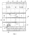
- a frill-color organic light-emitting display 100 is formed on a light transmissive and electrically insulative substrate 102.
- the portion of the display 100 is shown to have an array of light-emitting pixels P arranged at intersections between columns C1-C6 and rows R1-R3.
- Each pixel P is partitioned into sets of three subpixels R p , G p , and B p , designated to emit red, green, and blue light, respectively, from an organic electroluminescent medium EL.
- the sets of subpixels are arranged along corresponding subpixels columns designated at a, b, and c.
- Each subpixel column is electrically addressed to emit light by applying an electrical drive voltage between corresponding light transmissive subpixel column electrodes designated at 104 and row electrodes designated at 106, from a clocked drive voltage source (not shown) so as to commence the display of one frame of information at the intersection between a subpixel column position "a" of the column C1 and the row R1.
- the organic EL medium in this subpixel position R p would emit red light.
- a center line 107 is indicated between two adjacent laterally spaced subpixel column electrodes 104 (repeating sets of subpixel columns a, b, and c) and a center line 108 is indicated between adjacent laterally spaced row electrodes 106 of rows R1, R2, and R3.
- FIG. 2 the display 100 is shown in an enlarged cross sectional view taken along the lines 2-2 of FIG. 1.
- a set of three color subpixels R p , G p , and B p form the column C2 intersecting the row R3.
- a set (a, b, c) of light transmissive subpixel column electrodes 104 which are laterally spaced, as indicated by center line 107.
- an organic EL medium comprised of, in sequence, an organic hole-transporting layer 110, an organic light-emitting layer 120 which is also capable of transporting electrons, and an organic electron-transporting layer 130.
- a row electrode 106 corresponds to the row R3.
- the light-emitting layer 120 is formed of an organic light-emitting host material selected to emit light in a blue region of the visible spectrum (also referred to in abbreviated form as a blue spectral region), as will be described in more detail with reference to FIG. 4.
- the light-emitting layer 120 shows schematically three doped regions which are laterally aligned with respect to each of the corresponding subpixel columns a, b, and c, of the subpixel column electrodes 104.
- a red light-emitting dopant 125 is shown uniformly dispersed in the light-emitting layer 120 to provide the red subpixel R p .
- a green light-emitting dopant 127 is dispersed uniformly in the light-emitting layer 120 and in a pattern which is spatially centered over the subpixel electrode b to provide the green subpixel G p .
- a blue light-emitting dopant 129 is uniformly dispersed in the light-emitting layer 120 so as to modify or fine tune the hue of the blue light emitted from an undoped light-emitting organic light-emitting host material.
- a pixel P is defined as extending between center lines 108 of the laterally spaced row electrodes 106 at row R2.
- a monochrome host light-emitting display 100MH is shown in a cross sectional view similar to that depicted in FIG.3.
- the organic light-emitting layer 120 is formed of an undoped organic light-emitting host material.
- a junction 112 is formed at an interface between the hole-transporting layer 110 and the light-emitting layer 120 which is also capable of transporting electrons.
- the subpixel electrode 104 and the row electrode 106 of the row R2 are connected to an external power source 140 (drive voltage supply) by leads 144 and 146, respectively.
- the source 140 can be a continuous direct current or alternating current voltage source or an intermittent current voltage source.
- any convenient conventional power source including any desired switching circuitry, can be employed which is capable of sequentially addressing the subpixels of the display by biasing the subpixel column electrodes 104 (a, b, c, and so forth) positively with respect to the row electrodes 106 of rows R1, R2, R3, and so forth
- the internal junction 112 can be viewed as a diode which is forward biased when the subpixel column electrode is at a more positive potential than the row electrode 106 of the row R2, depicted here for illustrative purposes only. Under these conditions, injection of holes (positive charge carriers) occurs from the electrode 104 into the hole-transporting layer 110, while electrons (negative charge carriers) are injected from the electrode 106 into the organic electron-transporting layer 130. The injected holes and electrons each migrate toward the oppositely charged electrode, and hole-electron recombination occurs at or near the junction 112. When a migrating electron drops form its conduction band potential to a valance band in filling a hole, energy is released as light.
- the emitted light 165MH is reflective of the monochrome host material and is shown with straight arrows originating at or near the junction 112 and being transmitted through the light transmissive hole-transporting layer 110, the light transmissive subpixel electrode 104, and the light transmissive substrate 102 for viewing by an observer.
- the panel 100 is shown to have a dopant 125 uniformly dispersed within the light-emitting layer 120, the dopant selected to produce red light emission from the light -emitting layer, shown as emitted light 165 and indicated by wavy arrows.
- the light transmissive substrate 102 is electrically insulative and can be selected from glass, quartz, and plastic materials.
- the subpixel column electrodes 104 (a, b, c, and so forth) are formed of a subpixel material selected to provide hole injection from the electrodes 104 into the hole-transporting layer 110. Suitable materials include indium oxide, tin oxide, and indium tin oxide (ITO).
- the hole-transporting layer 110 is preferably formed over the sets of subpixel column electrodes and over the substrate by vapor depositing an organic hole-transporting material. In US-A-4,539,507, the hole-transporting material is preferably selected from the group consisting of aromatic tertiary amines.
- the organic light-emitting layer 120 can be formed by vapor depositing an organic light-emitting host material to a desired thickness.
- Particularly preferred host materials for forming the blue light-emitting layer 120 are metal chelated oxinoid compounds, as disclosed in US-A-4,769,292 cited above.
- Particularly preferred metal chelated oxinoid compounds are mixed ligand aluminum chelates as the type disclosed in US-A-5,150,006.
- the blue light-emitting layer 120 can be formed by solution coating of a polymeric organic blue light-emitting host material.
- polymeric blue light-emitting host materials suitable for solution coating include polyparaphenylene vinylenes (PPV), PPV copolymers, polyanilines, poly-3-alkylthiopenes, poly-3-octylthiopenes, and polyparaphenylenes.
- the electron-transporting layer 130 is preferably formed by vapor depositing an organic electron-transporting material which is also preferably a metal chelated oxinoid compound.
- the row electrodes 106 can be vapor deposited, and of a material selected to provide electron injection from each row electrode into the electron-transporting layer 130.
- particularly preferred row electrode materials are composite materials comprised of a low work function metal (a work function smaller than 4.0eV) and a second metal which preferably has a work function greater than 4.0eV, which includes metals more resistant to oxidation and which are therefore more commonly fabricated as metallic layers.
- the lateral spacing between the row electrodes 106 corresponding to the rows R1, R2, and R3 can be provided by depositing these electrodes from the vapor phase through apertures in a shadow mask positioned in close proximity to the electron-transporting layer 130, and having apertures corresponding to the row electrodes to be formed and oriented with respect to orientation marks (not shown) disposed around a peripheral region on the substrate 102.
- the lateral spacing between adjacent row electrodes can be provided by forming integral shadow masks on the substrate 102 and configured in a manner similar to the integral shadow mask walls described in US-A-5,294,869 and US-A-5,294,870.
- FIGS. 6A, 6B, and 6C the steps of the inventive method of forming a dopant layer by ink-jet printing over a light-emitting layer and diffusing the dopant from the dopant layer into the light-emitting layer are illustrated for a" red" dopant.
- an organic hole-transporting layer 110 has been formed over the subpixel column electrodes, and an undoped light-emitting host layer 120 has been formed over the hole-transporting layer.
- An ink-jet print head 800 of a commercially available ink-jet printer (not shown) provides a "red" dopant ink-jet 815 which is being scanned in a direction (normal to the plane of the drawing) along the subpixel column a and in alignment therewith to provide a growing dopant layer 122a (shown in dashed outline) of a "red" dopant over the light-emitting layer 120.
- FIG. 6B shows the completed dopant layer 122 containing the "red" dopant 125 shown in dotted outline, and formed in alignment with respect to the subpixel column a of the subpixel column electrodes 104.
- a dopant diffusing step is schematically indicated by dashed arrows 910 which represent a vapor of a fluid or of a fluid mixture selected to provide molecular diffusion paths in the light-emitting layer 120 so as to permit uniform diffusion of the dopant 125 from the dopant layer 122 into the light-emitting layer.
- the dopant 125 will diffuse laterally by a small distance (not shown) so that the lateral boundaries of the doped portion of the light-emitting layer 120 coincide with the center lines 107 of the lateral spacing between adjacent subpixel columns.
- the dopant 125 forms a red light-emitting subpixel column R p .
- FIGS. 7A-7D illustrate an alternative method of forming a dopant layer 122 over the light-emitting layer 120 (FIG. 7D).
- a dopant donor assembly 600 comprises a donor support 610 on which is printed by ink-jet printing a growing dopant donor layer 622a of a "red" dopant from an ink-jet 815.
- the completed dopant donor layer 622 is shown on the donor support 610 in FIG. 7B, and is comprised of the "red" dopant 625.
- the dopant donor assembly 600 is shown inverted and disposed in close proximity and substantially parallel to the surface of the light-emitting layer 120, and oriented or aligned with respect to orientation marks or alignment marks (not shown) disposed along a peripheral region of the substrate 102.
- heat radiation 680 is used to heat the donor support 610 so that the dopant donor layer 622 of FIG. 7C vaporizes or sublimes, thereby transferring the donor layer from the donor support 610 to the light-emitting layer 120 to form the dopant layer 122 thereon of the "red" dopant 125, and in alignment with the subpixel column a.
- the dopant diffusing step previously described with reference to FIG. 6C can now be used to diffuse the dopant 125 from the dopant layer 122 into the light-emitting layer 120 to form the red light-emitting subpixel column R p .
- FIGS. 8A-8E a sequence of process steps are shown in accordance with one aspect of the method of the present invention, in which a dopant layer 122 of a "red” dopant, a dopant layer 124 of "green” dopant, and a dopant layer 126 of "blue” dopant are formed sequentially by sequential ink-jet printing of these dopant layers over a light-emitting layer 120 (FIG.8D).
- an ink-jet print head 800 (shown in solid outline) first provides a "red” dopant ink-jet 815 to form a growing dopant layer 122a (shown in dashed outline) of a "red" dopant over the light-emitting layer and in alignment with respect to the subpixel column "a" shown at the left side of the drawing.
- the ink-jet print head 800 is then laterally translated as indicated by the dashed arrow 802 to a position (shown in dashed outline) for ink-jet printing a growing dopant layer 122a of the "red" dopant over the light-emitting layer 120, and in alignment with a subpixel column "a" of an adjacent set of subpixel columns, as shown at the far right location of the drawing.
- an ink-jet print head 800 provides a "green” dopant ink-jet 817 to form a growing dopant layer 124a of a "green” dopant and aligned with respect to subpixel columns b.
- an ink-jet print head 800 uses a "blue" dopant ink-jet 819 to form a growing dopant layer 126a of a "blue” dopant over the light-emitting layer 120, and in alignment with respective subpixel columns c.
- the dopant layers 122, 124, and 126 of FIG. 8D each contain at least one dopant.
- the dopant layer 122 of "red” dopant contains at least one "red” dopant 125
- the dopant layer 124 of"green” dopant contains at least one "green” dopant
- the dopant layer 126 of "blue” dopant contains at least one "blue” dopant 129.
- FIG. 8E indicates the dopant diffusing step in which the dopants 125, 127, and 129 are diffused together from the corresponding dopant layers 122, 124, and 126 as a pattern into the light-emitting layer 120 to be uniformly dispersed therein and to thereby provide the red light-emitting, green light-emitting, and blue light-emitting subcolumns R p , G p , and B p .
- Each of the ink-jets 815, 817, and 819 comprises an ink-jet printable composition which includes at least one printing fluid and at least one dopant.
- a printing fluid or a mixture of printing fluids is selected such that the fluid or fluids will not penetrate the light-emitting layer 120, and vapor or vapors of such printing fluid will not provide molecular diffusion paths for the dopant in the light-emitting layer.
- Aqueous printing fluids are preferred printing fluids because they are non-penetrating, and vapors of aqueous printing fluids do not provide molecular diffusion paths in a light-emitting layer.
- the dopant diffusing step is carried out by exposing the dopant layers and the light-emitting layer 120 to fluid vapor 910 in a vapor treatment system subsequent to ink-jet printing of the dopant layers.
- the dopant or dopants of each ink-jet printable composition are fluorescent dyes whose propensity for emitting light in response to hole-electron recombination has been well established in organic light-emitting devices of the prior art in which both a blue light-emitting host material and a fluorescent dopant were co-deposited from the vapor phase.
- fluorescent dyes suitable for formulating each of the ink-jet printable compositions are fluorescent dyes selected from dye classes consisting of coumarin, dicyanomethylenepyrans and thiopyrans, polymethine, oxabenzanthracene, xanthene, pyrylium and thiapyrylium, carbostyril, and perylene fluorescent dyes.
- the hue of light emission associated with each of the fluorescent dopants dispersed in the light-emitting layer 120 may be adjusted or fine tuned to meet or to exceed certain color standards for red, green, and blue light emitted from subpixels of the light-emitting display.
- color standards are frequently expressed in a so-called CIE color diagram as color coordinates.
- Each one of the ink-jet printable compositions is filled into a separate ink-jet printing cartridge (not shown) which is inserted into the ink-jet print head 800 in a well known manner.
- the ink-jet printing cartridge is removed form the ink-jet print head and an ink-jet printing cartridge containing the second dopant or dopants is inserted into the print head, and so forth.
- FIGS. 9A, 9B, and 9C a sequence of only three process steps is shown in a method of making a frill-color organic light-emitting display.
- This method differs from the aforementioned methods of first forming dopant layers over the light-emitting layer 120 by ink-jet printing of dopants and subsequently diffusing the dopants into the light-emitting layer, in that modified ink-jet printable compositions are formulated to include at least one printing fluid providing printing fluid vapors capable of forming molecular diffusion paths in the light-emitting layer 120 for diffusing the respective dopant into the light-emitting layer during the ink-jet printing step.
- a "red” dopant ink-jet 825 contains at least one printing fluid whose printing fluid vapor promotes diffusion of the "red” dopant 125 into the light-emitting layer.
- the "green" dopant ink-jet 827 and the “blue” dopant ink-jet 829 each derive from modified ink-jet printable compositions which include at least one printing fluid providing the printing fluid vapors to promote diffusion of the respective dopants into the light-emitting layer during the ink-jet printing step.
- Examples of printing fluids which, used alone or in a mixture of printing fluids, can provide vapors capable of forming molecular diffusion paths during the ink-jet printing step are alcohols such as butanol, ethanol, isopropanol, and methanol; ketones such as acetone, butanone, and methyl ethyl ketone; and chlorinated fluids such as dichloromethane.
- alcohols such as butanol, ethanol, isopropanol, and methanol
- ketones such as acetone, butanone, and methyl ethyl ketone
- chlorinated fluids such as dichloromethane.
- FIGS. 10A-10F a sequence of steps comprising a method of making a full-color organic light-emitting display in accordance with another aspect of the invention is shown.
- This method differs from the aforementioned methods in that dopant layers 122, 124, and 126 (see FIG.10D) are sequentially ink-jet printed over a hole-transporting layer 110 in a manner similar to the sequence of steps described with reference to FIGS. 8A-8D. Accordingly, no further description of the ink-jet printing of the layers will be required.
- an undoped light-emitting layer 120 is shown formed over the dopant layers 122, 124, and 126 and over the hole-transporting layer 110 within the lateral spacings between the respective dopant layers.
- fluid vapor 910 creates molecular diffusion paths in the light-emitting layer 120 and promotes diffusion of the respective dopants 125, 127, and 129 (see FIG. 10D) from the dopant layers into the overlying light-emitting layer, thereby forming the subpixel columns R p , G p , and B p .
- the doped light-emitting layer 120 could be lifted off the hole-transporting layer 110 when the dopant layers 122, 124, and 126 substantially vanish as their respective dopants diffuse upwardly into the light-emitting layer 120, it will be appreciated that the dopant layers are formed to a thickness in a range of 0.1 to 1nm (1-10 Angstrom), that is, to a thickness of molecular dimensions.
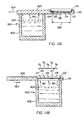
- a vapor treatment system 900 is schematically indicated comprising a container 902 which contains a vaporizable fluid to a level 904, the fluid producing a fluid vapor 910, shown by dashed arrows, in a volume extending between a sealed sliding cover 920 and the fluid level 904.
- the sliding cover has a recessed aperture 922 into which can be positioned a panel in preparation for diffusion of a dopant from a dopant layer or of dopants from a plurality of dopant layers into a light-emitting layer.
- a panel having a light-emitting layer 120 and overlying dopant layers 122, 124, and 126.
- the sliding cover has been translated by a sliding motion as indicated at 924, so as to expose the dopant layers and the light-emitting layer to the fluid vapor 910 for a defined period of time, and to thereby diffuse the dopants from the dopant layers into the light-emitting layer 120.
- a vapor treatment system can be readily constructed to control vapor formation within the container 902 by heating and/or cooling means (not shown) surrounding the interior or exterior of the container.
- fluids and fluid mixtures can be selected to provide fluid vapors useful for diffusing a dopant from a dopant layer or dopants from a plurality of dopant layers into a light-emitting layer at or near room temperature.
- fluids and fluid mixtures can be selected from among alcohols such as isopropanol; ketones, such as acetone and 2-butanone; and chlorinated fluids, such as dichloromethane.
- Example 1 The sample of Example 1 was further subjected to a dopant diffusion step in a vapor treatment system shown in FIGS. 11A and 11B, in acetone vapor for 7 seconds. Observation of photoluminescence as described in Example 1 provided the following results:
- forming the electron-transporting layer includes vapor depositing an organic electron-transporting material selected from the group consisting of metal chelated oxinoid compounds.
- the method of making a full-color organic light-emitting display wherein forming the second set of addressing electrode layer includes vapor depositing electrodes and of a material selected to provide electron injection from the electrodes of the second set into the electron-transporting layer.
- a method of making a full-color organic light-emitting display having an array of light-emitting pixels arranged in intersecting columns and rows with each column having a set of three subpixel columns designated for emitting one of red, green, and blue light respectively, the method comprising the steps of:
- the method of making a full-color organic light-emitting display wherein forming the hole-transporting layer includes vapor depositing an organic hole-transporting material selected from the group consisting of aromatic tertiary amines.
- the method of making a full-color organic light-emitting display wherein sequentially forming a dopant layer includes sequentially ink-jet printing the at least one first, second, and third dopants.
- the method of making a full-color organic light-emitting display wherein the dopant layer ink-jet printing step includes the steps of:
- the method of making a full-color organic light-emitting display wherein the step of formulating the ink-jet printable composition includes selecting at least one fluorescent dye as the at least one first, second, or third dopant.
- the method of making a full-color organic light-emitting display wherein the fluorescent dye selecting step includes choosing a fluorescent dye selected from the class consisting of coumarin, dicyanomethylenepyrans and thiopyrans, polymethine, oxzbenzanthracene, xanthene, pyrylium and thiapyrylium, carbostyril, and perylene fluorescent dyes.
- the method of making a full-color organic light-emitting display wherein the step of sequentially forming a dopant layer includes the steps of:
- the method of making a full-color organic light-emitting display wherein the light-emitting layer forming step includes vapor depositing an organic light-emitting host material selected from the group consisting of metal chelated oxinoid compounds.
- the method of making a full-color organic light-emitting display wherein the step of diffusing the first, second, and third dopants together includes exposing the light-emitting layer and the dopant layers to vapor of a fluid or of a fluid mixture selected to provide molecular diffusion paths in the light-emitting layer which permit uniform diffusion of the dopants as patterns into the host material of the light-emitting layer.
- the method of making a full-color organic light-emitting display wherein the electron-transporting layer forming step includes vapor depositing an organic electron-transporting material selected from the group consisting of metal chelated oxinoid compounds.
- the method of making a full-color organic light-emitting display wherein the row electrode-disposing step includes vapor depositing row electrodes and of a material selected to provide electron injection from the row electrodes into the electron-transporting layer.
- a method of making a full-color organic light-emitting display having an array of light-emitting pixels arranged in intersecting columns and rows with each column having a set of three subpixel columns designated for emitting one of red, green, and blue light respectively, the method comprising the steps of
- a method of making a full-color organic light-emitting display having an array of light-emitting pixels arranged in intersecting columns and rows with each column having a set of three subpixel columns designated for emitting one of red, green, and blue light respectively, the method comprising the steps of:
- the method of making a full-color organic light-emitting display wherein forming the hole-transporting layer includes vapor depositing an organic hole-transporting material selected from the group consisting of aromatic tertiary amines.
- the method of making a full-color organic light-emitting display wherein forming the light-emitting layer includes vapor depositing an organic light-emitting host material selected from the group consisting of metal chelated oxinoid compounds.
- the method of making a full-color organic light-emitting display wherein forming the light-emitting layer includes solution coating a polymeric organic light-emitting host material selected from the group consisting of polyparaphenylene vinylene (PPV), PPV copolymers, polyanilines, poly-3-alkylthiopenes, poly-3-octylthiopenes, and polyparaphenylenes.
- a polymeric organic light-emitting host material selected from the group consisting of polyparaphenylene vinylene (PPV), PPV copolymers, polyanilines, poly-3-alkylthiopenes, poly-3-octylthiopenes, and polyparaphenylenes.
- the method of making a full-color organic light-emitting display wherein dopant layer ink-jet printing includes the steps of:
- the method of making a full-color organic light-emitting display wherein the step of formulating the ink-jet printable composition includes selecting at least one fluorescent dye as the at least one first, second, or third dopant.
- the method of making a full-color organic light-emitting display wherein selecting the fluorescent dye includes choosing a fluorescent dye selected from the class consisting of coumarin, dicyanomethylenepyrans and thiopyrans, polymethine, oxabenzanthracene, xanthene, pyrylium and thiapyrylium, carbostyril, and perylene fluorescent dyes.
- the method of making a full-color organic light-emitting display wherein the step of diffusing the first, second, and third dopants together includes exposing the dopant layers and the light-emitting layer to vapor of a fluid or of a fluid mixture selected to provide molecular diffusion paths in the light-emitting layer which permit uniform diffusion of the dopants as patterns into the host material of the light-emitting layer.
- the method of making a full-color organic light-emitting display wherein forming the electron-transporting layer includes vapor depositing an organic electron-transporting material selected from the group consisting of metal chelated oxinoid compounds.
- the method of making a full-color organic light-emitting display wherein the row electrode-disposing step includes vapor depositing row electrodes and of a material selected to provide electron injection from the row electrodes into the electron-transporting layer.
- a method of making a full-color organic light-emitting display having an array of light-emitting pixels arranged in intersecting columns and rows with each column having a set of three subpixel columns designated for emitting one of red, green, and blue light respectively, the method comprising the steps of:
- a method of making a full-color organic light-emitting display having an array of light-emitting pixels arranged in intersecting columns and rows with each column having a set of three subpixel columns designated for emitting one of red, green, and blue light respectively, the method comprising the steps of:
- the method of making a frill-color organic light-emitting display wherein the hole-transporting layer forming step includes vapor depositing an organic hole-transporting material selected from the group consisting of aromatic tertiary amines.
- the method of making a frill-color organic light-emitting display wherein the light-emitting layer forming step includes vapor depositing an organic light-emitting host material selected from the group consisting of metal chelated oxinoid compounds.
- the method of making a full-color organic light-emitting display wherein the light-emitting layer forming step includes solution coating a polymeric organic light-emitting host material selected from the group consisting of polyparaphenylene vinylene (PPV), PPV copolymers, polyanilines, poly-3-alkylthiopenes, poly-3-octylthiopenes, and polyparaphenylenes.
- PPV polyparaphenylene vinylene
- PPV copolymers polyanilines
- poly-3-alkylthiopenes poly-3-octylthiopenes
- polyparaphenylenes polyparaphenylenes
- the method of making a full-color organic light-emitting display wherein the step of sequentially forming a dopant layer includes sequentially ink-jet printing the at least one first, second, and third dopants.
- the method of making a full-color organic light-emitting display wherein the dopant layer ink-jet printing step includes the steps of:
- the method of making a full-color organic light-emitting display wherein the step of formulating the ink-jet printable composition includes selecting at least one fluorescent dye as the at least one first, second, or third dopant.
- the method of making a full-color organic light-emitting display wherein selecting the fluorescent dye includes choosing a fluorescent dye selected from the class consisting of coumarin, dicyanomethylenepyrans and thiopyrans, polymethine, oxabenzanthracene, xanthene, pyrylium and thiapyrylium, carbostyril, and perylene fluorescent dyes.
- the method of making a full-color organic light-emitting display wherein sequentially forming a dopant layer includes the steps of:
- the method of making a full-color organic light-emitting display wherein diffusing the first, second, and third dopants together includes exposing the dopant layers and the light-emitting layer to vapor of a fluid or of a fluid mixture selected to provide molecular diffusion paths in the light-emitting layer which permit uniform diffusion of the dopant as patterns into the light-emitting material of the light-emitting layer.
- the method of making a full-color organic light-emitting display wherein forming the electron-transporting layer includes vapor depositing an organic electron-transporting material selected from the group consisting of metal chelated oxinoid compounds.
- the method of making a full-color organic light-emitting display wherein the row electrode-disposing step includes vapor depositing row electrodes and of a material selected to provide electron injection from the row electrodes into the electron-transporting layer.
Landscapes
- Electroluminescent Light Sources (AREA)
Applications Claiming Priority (2)
| Application Number | Priority Date | Filing Date | Title |
|---|---|---|---|
| US217729 | 1988-07-07 | ||
| US09/217,729 US6066357A (en) | 1998-12-21 | 1998-12-21 | Methods of making a full-color organic light-emitting display |
Publications (2)
| Publication Number | Publication Date |
|---|---|
| EP1014458A2 true EP1014458A2 (fr) | 2000-06-28 |
| EP1014458A3 EP1014458A3 (fr) | 2004-01-28 |
Family
ID=22812264
Family Applications (1)
| Application Number | Title | Priority Date | Filing Date |
|---|---|---|---|
| EP99204212A Withdrawn EP1014458A3 (fr) | 1998-12-21 | 1999-12-09 | Procédés de fabrication d'une matrice d'affichage électroluminescente organique en couleur |
Country Status (4)
| Country | Link |
|---|---|
| US (1) | US6066357A (fr) |
| EP (1) | EP1014458A3 (fr) |
| JP (1) | JP2000188180A (fr) |
| KR (1) | KR20000048257A (fr) |
Cited By (2)
| Publication number | Priority date | Publication date | Assignee | Title |
|---|---|---|---|---|
| WO2005004253A1 (fr) * | 2003-06-24 | 2005-01-13 | Eastman Kodak Company | Affichage electroluminescent organique comprenant un colorant luminescent modifie de maniere a etre luminescent a diverses longueurs d'ondes desirees |
| CN102208432A (zh) * | 2010-03-29 | 2011-10-05 | Tdk株式会社 | 透射式彩色有机el显示装置 |
Families Citing this family (166)
| Publication number | Priority date | Publication date | Assignee | Title |
|---|---|---|---|---|
| US7090890B1 (en) * | 1998-04-13 | 2006-08-15 | The Trustees Of Princeton University | Modification of polymer optoelectronic properties after film formation by impurity addition or removal |
| US6566153B1 (en) * | 1998-10-14 | 2003-05-20 | The Regents Of The University Of California | Process for fabricating organic semiconductor devices using ink-jet printing technology and device and system employing same |
| WO2001026425A1 (fr) * | 1999-10-05 | 2001-04-12 | Matsushita Electric Industrial Co., Ltd. | Dispositif electroluminescent et procede de fabrication correspondant, et afficheur et dispositif d'eclairage comprenant ledit dispositif |
| KR100721656B1 (ko) * | 2005-11-01 | 2007-05-23 | 주식회사 엘지화학 | 유기 전기 소자 |
| US7221088B2 (en) * | 2000-11-29 | 2007-05-22 | The United States Of America As Represented By The Secretary Of The Navy | Universal host for RG or RGB emission in organic light emitting devices |
| CN101397649B (zh) * | 2001-02-01 | 2011-12-28 | 株式会社半导体能源研究所 | 能够将有机化合物沉积在衬底上的装置 |
| US6762124B2 (en) | 2001-02-14 | 2004-07-13 | Avery Dennison Corporation | Method for patterning a multilayered conductor/substrate structure |
| US20020110673A1 (en) | 2001-02-14 | 2002-08-15 | Ramin Heydarpour | Multilayered electrode/substrate structures and display devices incorporating the same |
| JP2003022892A (ja) * | 2001-07-06 | 2003-01-24 | Semiconductor Energy Lab Co Ltd | 発光装置の製造方法 |
| EP1289015B1 (fr) * | 2001-08-28 | 2012-05-23 | Konica Corporation | Dispositif émetteur de lumière en plusieurs couleurs et procédé de production de ce dispositif |
| US7744957B2 (en) * | 2003-10-23 | 2010-06-29 | The Trustees Of Princeton University | Method and apparatus for depositing material |
| US7431968B1 (en) * | 2001-09-04 | 2008-10-07 | The Trustees Of Princeton University | Process and apparatus for organic vapor jet deposition |
| US7404862B2 (en) * | 2001-09-04 | 2008-07-29 | The Trustees Of Princeton University | Device and method for organic vapor jet deposition |
| US8535759B2 (en) * | 2001-09-04 | 2013-09-17 | The Trustees Of Princeton University | Method and apparatus for depositing material using a dynamic pressure |
| GB2379412A (en) * | 2001-09-10 | 2003-03-12 | Seiko Epson Corp | Deposition of soluble materials |
| US6579237B1 (en) | 2001-12-14 | 2003-06-17 | Koninklijke Philips Electronics Nv | Diagnostic ultrasonic imaging system having organic light emitting device display |
| JP4066661B2 (ja) * | 2002-01-23 | 2008-03-26 | セイコーエプソン株式会社 | 有機el装置の製造装置および液滴吐出装置 |
| US6872472B2 (en) | 2002-02-15 | 2005-03-29 | Eastman Kodak Company | Providing an organic electroluminescent device having stacked electroluminescent units |
| JP3925257B2 (ja) * | 2002-03-15 | 2007-06-06 | セイコーエプソン株式会社 | 気密チャンバにおける接続ラインの貫通構造およびこれを備えた吐出装置、並びに液晶表示装置の製造方法、有機el装置の製造方法、電子放出装置の製造方法、pdp装置の製造方法、電気泳動表示装置の製造方法、カラーフィルタの製造方法、有機elの製造方法、スペーサ形成方法、金属配線形成方法、レンズ形成方法、レジスト形成方法および光拡散体形成方法 |
| US6770502B2 (en) * | 2002-04-04 | 2004-08-03 | Eastman Kodak Company | Method of manufacturing a top-emitting OLED display device with desiccant structures |
| US6811815B2 (en) * | 2002-06-14 | 2004-11-02 | Avery Dennison Corporation | Method for roll-to-roll deposition of optically transparent and high conductivity metallic thin films |
| US7176617B2 (en) * | 2002-07-01 | 2007-02-13 | Seiko Epson Corporation | Composition, method of forming film, film formation device, electro-optical device, method of manufacturing the same, organic electroluminescent device, method of manufacturing the same, device and method of manufacturing the same, and electronic apparatus |
| TW200402012A (en) * | 2002-07-23 | 2004-02-01 | Eastman Kodak Co | OLED displays with fiber-optic faceplates |
| US6747618B2 (en) | 2002-08-20 | 2004-06-08 | Eastman Kodak Company | Color organic light emitting diode display with improved lifetime |
| US20040043138A1 (en) * | 2002-08-21 | 2004-03-04 | Ramesh Jagannathan | Solid state lighting using compressed fluid coatings |
| US20040043140A1 (en) * | 2002-08-21 | 2004-03-04 | Ramesh Jagannathan | Solid state lighting using compressed fluid coatings |
| US7098060B2 (en) | 2002-09-06 | 2006-08-29 | E.I. Du Pont De Nemours And Company | Methods for producing full-color organic electroluminescent devices |
| US6911671B2 (en) | 2002-09-23 | 2005-06-28 | Eastman Kodak Company | Device for depositing patterned layers in OLED displays |
| US7067170B2 (en) * | 2002-09-23 | 2006-06-27 | Eastman Kodak Company | Depositing layers in OLED devices using viscous flow |
| US6765349B2 (en) * | 2002-09-30 | 2004-07-20 | Eastman Kodak Company | High work function metal alloy cathode used in organic electroluminescent devices |
| US6831407B2 (en) * | 2002-10-15 | 2004-12-14 | Eastman Kodak Company | Oled device having improved light output |
| US6982179B2 (en) * | 2002-11-15 | 2006-01-03 | University Display Corporation | Structure and method of fabricating organic devices |
| US20040096570A1 (en) * | 2002-11-15 | 2004-05-20 | Michael Weaver | Structure and method of fabricating organic devices |
| KR100650046B1 (ko) * | 2002-11-20 | 2006-11-27 | 엘지전자 주식회사 | 고효율의 유기 전계 발광 소자 |
| US7230594B2 (en) | 2002-12-16 | 2007-06-12 | Eastman Kodak Company | Color OLED display with improved power efficiency |
| US20040196318A1 (en) * | 2003-04-01 | 2004-10-07 | Su Massharudin Bin | Method of depositing phosphor on light emitting diode |
| US7514149B2 (en) * | 2003-04-04 | 2009-04-07 | Corning Incorporated | High-strength laminated sheet for optical applications |
| US6841270B2 (en) | 2003-04-17 | 2005-01-11 | Canon Kabushiki Kaisha | Organic light-emitting device having pyrylium salt as charge transport material |
| JP4285741B2 (ja) * | 2003-10-24 | 2009-06-24 | 独立行政法人産業技術総合研究所 | 有機電界発光素子およびその作製方法 |
| US20050100657A1 (en) * | 2003-11-10 | 2005-05-12 | Macpherson Charles D. | Organic material with a region including a guest material and organic electronic devices incorporating the same |
| EP1683214B1 (fr) * | 2003-11-10 | 2007-03-21 | E.I. Dupont De Nemours And Company | Procede de formation de couches organiques presentant une zone qui comprend un materiau invite et dispositifs electroniques organiques comportant ledit materiau |
| US7221332B2 (en) * | 2003-12-19 | 2007-05-22 | Eastman Kodak Company | 3D stereo OLED display |
| US7011529B2 (en) * | 2004-03-01 | 2006-03-14 | Anritsu Company | Hermetic glass bead assembly having high frequency compensation |
| US7067841B2 (en) * | 2004-04-22 | 2006-06-27 | E. I. Du Pont De Nemours And Company | Organic electronic devices |
| US20050253917A1 (en) * | 2004-05-13 | 2005-11-17 | Quanyuan Shang | Method for forming color filters in flat panel displays by inkjetting |
| US20050255253A1 (en) * | 2004-05-13 | 2005-11-17 | White John M | Apparatus and methods for curing ink on a substrate using an electron beam |
| US20060017055A1 (en) * | 2004-07-23 | 2006-01-26 | Eastman Kodak Company | Method for manufacturing a display device with low temperature diamond coatings |
| US20060022174A1 (en) * | 2004-07-27 | 2006-02-02 | General Electric Company | Electroactive chemical composition and method of coating |
| DE102004042356A1 (de) * | 2004-09-01 | 2006-03-02 | Siemens Ag | Anzeigeeinheit und Verfahren zur Herstellung einer Anzeigeeinheit |
| US9040170B2 (en) * | 2004-09-20 | 2015-05-26 | Global Oled Technology Llc | Electroluminescent device with quinazoline complex emitter |
| US20060092218A1 (en) * | 2004-11-04 | 2006-05-04 | Applied Materials, Inc. | Methods and apparatus for inkjet printing |
| US20060093751A1 (en) * | 2004-11-04 | 2006-05-04 | Applied Materials, Inc. | System and methods for inkjet printing for flat panel displays |
| US20060109296A1 (en) * | 2004-11-04 | 2006-05-25 | Bassam Shamoun | Methods and apparatus for inkjet printing color filters for displays |
| US7413272B2 (en) * | 2004-11-04 | 2008-08-19 | Applied Materials, Inc. | Methods and apparatus for precision control of print head assemblies |
| US20070042113A1 (en) * | 2004-11-04 | 2007-02-22 | Applied Materials, Inc. | Methods and apparatus for inkjet printing color filters for displays using pattern data |
| US7556334B2 (en) * | 2004-11-04 | 2009-07-07 | Applied Materials, Inc. | Methods and apparatus for aligning print heads |
| US20060131505A1 (en) * | 2004-12-17 | 2006-06-22 | Eastman Kodak Company | Imaging element |
| US7515149B2 (en) * | 2004-12-17 | 2009-04-07 | Eastman Kodak Company | Display with wirelessly controlled illumination |
| US7538756B2 (en) * | 2004-12-17 | 2009-05-26 | Eastman Kodak Company | Methods for making display |
| US20060136734A1 (en) * | 2004-12-21 | 2006-06-22 | Eastman Kodak Company | Identification display device |
| US20060136997A1 (en) * | 2004-12-21 | 2006-06-22 | Eastman Kodak Company | Authentication system and method |
| US20060131393A1 (en) * | 2004-12-22 | 2006-06-22 | Eastman Kodak Company | Multi-role transaction card |
| US7268006B2 (en) | 2004-12-30 | 2007-09-11 | E.I. Du Pont De Nemours And Company | Electronic device including a guest material within a layer and a process for forming the same |
| US20060159843A1 (en) * | 2005-01-18 | 2006-07-20 | Applied Materials, Inc. | Method of substrate treatment for manufacturing of color filters by inkjet printing systems |
| US7630029B2 (en) * | 2005-02-16 | 2009-12-08 | Industrial Technology Research Institute | Conductive absorption layer for flexible displays |
| US20060185587A1 (en) * | 2005-02-18 | 2006-08-24 | Applied Materials, Inc. | Methods and apparatus for reducing ink conglomerates during inkjet printing for flat panel display manufacturing |
| US8057916B2 (en) * | 2005-04-20 | 2011-11-15 | Global Oled Technology, Llc. | OLED device with improved performance |
| US20060240281A1 (en) * | 2005-04-21 | 2006-10-26 | Eastman Kodak Company | Contaminant-scavenging layer on OLED anodes |
| US20060273713A1 (en) * | 2005-06-02 | 2006-12-07 | Eastman Kodak Company | Process for making an organic light-emitting device |
| US20070001927A1 (en) * | 2005-07-01 | 2007-01-04 | Eastman Kodak Company | Tiled display for electronic signage |
| US7544723B2 (en) * | 2005-07-15 | 2009-06-09 | Applied Materials, Inc. | Blue printing ink for color filter applications |
| US7460267B2 (en) * | 2005-07-15 | 2008-12-02 | Applied Materials, Inc. | Green printing ink for color filter applications |
| US7532181B2 (en) * | 2005-07-20 | 2009-05-12 | Eastman Kodak Company | Visible and invisible image display |
| TWI318685B (en) * | 2005-07-28 | 2009-12-21 | Applied Materials Inc | Methods and apparatus for concurrent inkjet printing and defect inspection |
| US20070096640A1 (en) * | 2005-08-19 | 2007-05-03 | Gang Yu | Methods for producing full color organic electroluminescent devices |
| US20070048545A1 (en) * | 2005-08-31 | 2007-03-01 | Eastman Kodak Company | Electron-transporting layer for white OLED device |
| JP2007110067A (ja) * | 2005-09-14 | 2007-04-26 | Fujifilm Corp | 有機電界発光素子用組成物、有機電界発光素子の製造方法、及び有機電界発光素子 |
| US20070070132A1 (en) * | 2005-09-27 | 2007-03-29 | Fan-Cheung Sze | Inkjet delivery module |
| US20070068560A1 (en) * | 2005-09-29 | 2007-03-29 | Quanyuan Shang | Methods and apparatus for inkjet print head cleaning |
| US7611217B2 (en) * | 2005-09-29 | 2009-11-03 | Applied Materials, Inc. | Methods and systems for inkjet drop positioning |
| US20070070109A1 (en) * | 2005-09-29 | 2007-03-29 | White John M | Methods and systems for calibration of inkjet drop positioning |
| US20080018677A1 (en) * | 2005-09-29 | 2008-01-24 | White John M | Methods and apparatus for inkjet print head cleaning using an inflatable bladder |
| US20070076040A1 (en) * | 2005-09-29 | 2007-04-05 | Applied Materials, Inc. | Methods and apparatus for inkjet nozzle calibration |
| US20070085837A1 (en) * | 2005-10-17 | 2007-04-19 | Eastman Kodak Company | Touch input device with display front |
| US20070085838A1 (en) | 2005-10-17 | 2007-04-19 | Ricks Theodore K | Method for making a display with integrated touchscreen |
| US8956738B2 (en) * | 2005-10-26 | 2015-02-17 | Global Oled Technology Llc | Organic element for low voltage electroluminescent devices |
| US20070122657A1 (en) * | 2005-11-30 | 2007-05-31 | Eastman Kodak Company | Electroluminescent device containing a phenanthroline derivative |
| US9666826B2 (en) * | 2005-11-30 | 2017-05-30 | Global Oled Technology Llc | Electroluminescent device including an anthracene derivative |
| DE102005058557A1 (de) * | 2005-12-08 | 2007-06-14 | Merck Patent Gmbh | Organische Elektrolumineszenzvorrichtung |
| US7601567B2 (en) * | 2005-12-13 | 2009-10-13 | Samsung Mobile Display Co., Ltd. | Method of preparing organic thin film transistor, organic thin film transistor, and organic light-emitting display device including the organic thin film transistor |
| US8680693B2 (en) * | 2006-01-18 | 2014-03-25 | Lg Chem. Ltd. | OLED having stacked organic light-emitting units |
| GB2434915A (en) * | 2006-02-03 | 2007-08-08 | Cdt Oxford Ltd | Phosphoescent OLED for full colour display |
| GB2434916A (en) * | 2006-02-03 | 2007-08-08 | Cdt Oxford Ltd | OLED for full colour display |
| TWI328520B (en) * | 2006-02-07 | 2010-08-11 | Applied Materials Inc | Methods and apparatus for reducing irregularities in color filters |
| US20070207345A1 (en) * | 2006-03-01 | 2007-09-06 | Eastman Kodak Company | Electroluminescent device including gallium complexes |
| US9118020B2 (en) * | 2006-04-27 | 2015-08-25 | Global Oled Technology Llc | Electroluminescent devices including organic eil layer |
| US20070256709A1 (en) * | 2006-04-29 | 2007-11-08 | Quanyuan Shang | Methods and apparatus for operating an inkjet printing system |
| US20070252863A1 (en) * | 2006-04-29 | 2007-11-01 | Lizhong Sun | Methods and apparatus for maintaining inkjet print heads using parking structures with spray mechanisms |
| US20070263026A1 (en) * | 2006-04-29 | 2007-11-15 | Quanyuan Shang | Methods and apparatus for maintaining inkjet print heads using parking structures |
| EP2016633A1 (fr) | 2006-05-08 | 2009-01-21 | Eastman Kodak Company | Couche d'injection d'electrons d'une oled |
| US7992956B2 (en) * | 2006-06-07 | 2011-08-09 | Applied Materials, Inc. | Systems and methods for calibrating inkjet print head nozzles using light transmittance measured through deposited ink |
| US20080024548A1 (en) * | 2006-07-26 | 2008-01-31 | Applied Materials, Inc. | Methods and apparatus for purging a substrate during inkjet printing |
| US20080024532A1 (en) * | 2006-07-26 | 2008-01-31 | Si-Kyoung Kim | Methods and apparatus for inkjet printing system maintenance |
| WO2008013902A2 (fr) * | 2006-07-28 | 2008-01-31 | Applied Materials, Inc. | Procédés et appareils pour une fabrication perfectionnée de filtres de couleur |
| JP4993973B2 (ja) * | 2006-09-08 | 2012-08-08 | 株式会社ジャパンディスプレイイースト | 液晶表示装置 |
| JP2008171800A (ja) | 2006-10-31 | 2008-07-24 | Fei Co | 荷電粒子ビーム処理用保護層 |
| US20080131587A1 (en) * | 2006-11-30 | 2008-06-05 | Boroson Michael L | Depositing organic material onto an oled substrate |
| US20080204501A1 (en) * | 2006-12-01 | 2008-08-28 | Shinichi Kurita | Inkjet print head pressure regulator |
| US8795855B2 (en) | 2007-01-30 | 2014-08-05 | Global Oled Technology Llc | OLEDs having high efficiency and excellent lifetime |
| US7857413B2 (en) | 2007-03-01 | 2010-12-28 | Applied Materials, Inc. | Systems and methods for controlling and testing jetting stability in inkjet print heads |
| US20080284318A1 (en) * | 2007-05-17 | 2008-11-20 | Deaton Joseph C | Hybrid fluorescent/phosphorescent oleds |
| US20080284317A1 (en) * | 2007-05-17 | 2008-11-20 | Liang-Sheng Liao | Hybrid oled having improved efficiency |
| US8034465B2 (en) * | 2007-06-20 | 2011-10-11 | Global Oled Technology Llc | Phosphorescent oled having double exciton-blocking layers |
| KR101672553B1 (ko) * | 2007-06-25 | 2016-11-03 | 큐디 비젼, 인크. | 조성물 및 나노물질의 침착을 포함하는 방법 |
| US20090004485A1 (en) * | 2007-06-27 | 2009-01-01 | Shiying Zheng | 6-member ring structure used in electroluminescent devices |
| US7637587B2 (en) * | 2007-08-29 | 2009-12-29 | Applied Materials, Inc. | System and method for reliability testing and troubleshooting inkjet printers |
| JP5669580B2 (ja) * | 2007-09-20 | 2015-02-12 | ビーエーエスエフ ソシエタス・ヨーロピアBasf Se | エレクトロルミネセンスデバイス |
| US8498464B2 (en) * | 2007-09-27 | 2013-07-30 | Siemens Medical Solutions Usa, Inc. | Intrinsic co-registration for modular multimodality medical imaging systems |
| US20090091242A1 (en) * | 2007-10-05 | 2009-04-09 | Liang-Sheng Liao | Hole-injecting layer in oleds |
| US8129039B2 (en) | 2007-10-26 | 2012-03-06 | Global Oled Technology, Llc | Phosphorescent OLED device with certain fluoranthene host |
| US8431242B2 (en) * | 2007-10-26 | 2013-04-30 | Global Oled Technology, Llc. | OLED device with certain fluoranthene host |
| US8076009B2 (en) * | 2007-10-26 | 2011-12-13 | Global Oled Technology, Llc. | OLED device with fluoranthene electron transport materials |
| US20090110956A1 (en) * | 2007-10-26 | 2009-04-30 | Begley William J | Oled device with electron transport material combination |
| US8420229B2 (en) * | 2007-10-26 | 2013-04-16 | Global OLED Technologies LLC | OLED device with certain fluoranthene light-emitting dopants |
| US20090130296A1 (en) * | 2007-11-15 | 2009-05-21 | Universal Display Corporation | Fabrication of Organic Electronic Devices by Ink-Jet Printing at Low Temperatures |
| US8900722B2 (en) | 2007-11-29 | 2014-12-02 | Global Oled Technology Llc | OLED device employing alkali metal cluster compounds |
| WO2009076248A1 (fr) * | 2007-12-06 | 2009-06-18 | Applied Materials, Inc. | Systèmes et procédés pour améliorer la mesure d'une transmittance de lumière à travers de l'encre déposée sur un substrat |
| KR20100110323A (ko) * | 2007-12-06 | 2010-10-12 | 어플라이드 머티어리얼스, 인코포레이티드 | 라인 스캔 카메라를 사용하여 기판 상의 픽셀 웰들에 증착된 잉크를 측정하기 위한 방법 및 장치 |
| US20090162612A1 (en) * | 2007-12-19 | 2009-06-25 | Hatwar Tukaram K | Oled device having two electron-transport layers |
| US20090191427A1 (en) * | 2008-01-30 | 2009-07-30 | Liang-Sheng Liao | Phosphorescent oled having double hole-blocking layers |
| US7947974B2 (en) * | 2008-03-25 | 2011-05-24 | Global Oled Technology Llc | OLED device with hole-transport and electron-transport materials |
| US20090251504A1 (en) * | 2008-03-31 | 2009-10-08 | Applied Materials, Inc. | Systems and methods for wet in-situ calibration using measurement of light transmittance through ink deposited on a substrate |
| US8324800B2 (en) * | 2008-06-12 | 2012-12-04 | Global Oled Technology Llc | Phosphorescent OLED device with mixed hosts |
| CN101320772B (zh) * | 2008-07-15 | 2010-06-02 | 电子科技大学 | 用于led封装的荧光粉分散体的制备及喷墨打印方法 |
| US8247088B2 (en) * | 2008-08-28 | 2012-08-21 | Global Oled Technology Llc | Emitting complex for electroluminescent devices |
| JP2010061822A (ja) * | 2008-09-01 | 2010-03-18 | Seiko Epson Corp | 有機el装置の製造方法 |
| EP2161272A1 (fr) | 2008-09-05 | 2010-03-10 | Basf Se | Phénanthrolines |
| US7931975B2 (en) * | 2008-11-07 | 2011-04-26 | Global Oled Technology Llc | Electroluminescent device containing a flouranthene compound |
| US8088500B2 (en) * | 2008-11-12 | 2012-01-03 | Global Oled Technology Llc | OLED device with fluoranthene electron injection materials |
| US7968215B2 (en) * | 2008-12-09 | 2011-06-28 | Global Oled Technology Llc | OLED device with cyclobutene electron injection materials |
| US8216697B2 (en) * | 2009-02-13 | 2012-07-10 | Global Oled Technology Llc | OLED with fluoranthene-macrocyclic materials |
| US8147989B2 (en) * | 2009-02-27 | 2012-04-03 | Global Oled Technology Llc | OLED device with stabilized green light-emitting layer |
| US20100244677A1 (en) * | 2009-03-31 | 2010-09-30 | Begley William J | Oled device containing a silyl-fluoranthene derivative |
| US8206842B2 (en) | 2009-04-06 | 2012-06-26 | Global Oled Technology Llc | Organic element for electroluminescent devices |
| CN102482574B (zh) | 2009-06-18 | 2014-09-24 | 巴斯夫欧洲公司 | 用作场致发光器件的空穴传输材料的菲并唑化合物 |
| US20110014739A1 (en) * | 2009-07-16 | 2011-01-20 | Kondakov Denis Y | Making an emissive layer for multicolored oleds |
| US8877356B2 (en) * | 2009-07-22 | 2014-11-04 | Global Oled Technology Llc | OLED device with stabilized yellow light-emitting layer |
| US8801856B2 (en) * | 2009-09-08 | 2014-08-12 | Universal Display Corporation | Method and system for high-throughput deposition of patterned organic thin films |
| US8242489B2 (en) | 2009-12-17 | 2012-08-14 | Global Oled Technology, Llc. | OLED with high efficiency blue light-emitting layer |
| US8288187B2 (en) * | 2010-01-20 | 2012-10-16 | Universal Display Corporation | Electroluminescent devices for lighting applications |
| SG189560A1 (en) | 2011-10-11 | 2013-05-31 | 3M Innovative Properties Co | A display device |
| US9700908B2 (en) | 2012-12-27 | 2017-07-11 | Kateeva, Inc. | Techniques for arrayed printing of a permanent layer with improved speed and accuracy |
| US9352561B2 (en) | 2012-12-27 | 2016-05-31 | Kateeva, Inc. | Techniques for print ink droplet measurement and control to deposit fluids within precise tolerances |
| KR20190123811A (ko) | 2012-12-27 | 2019-11-01 | 카티바, 인크. | 정밀 공차 내로 유체를 증착하기 위한 인쇄 잉크 부피 제어를 위한 기법 |
| US12330178B2 (en) | 2012-12-27 | 2025-06-17 | Kateeva, Inc. | Techniques for arrayed printing of a permanent layer with improved speed and accuracy |
| US11141752B2 (en) | 2012-12-27 | 2021-10-12 | Kateeva, Inc. | Techniques for arrayed printing of a permanent layer with improved speed and accuracy |
| US11673155B2 (en) | 2012-12-27 | 2023-06-13 | Kateeva, Inc. | Techniques for arrayed printing of a permanent layer with improved speed and accuracy |
| US10593886B2 (en) | 2013-08-25 | 2020-03-17 | Molecular Glasses, Inc. | OLED devices with improved lifetime using non-crystallizable molecular glass mixture hosts |
| US10461269B2 (en) * | 2013-12-20 | 2019-10-29 | Molecular Glasses, Inc. | Crosslinkable, /polymerizable and combinations thereof charge-transporting molecular glass mixtures, luminescent molecular glass mixtures, or combinations thereof for organic light emitting diodes and other organic electronics and photonics applications and method of making same |
| US20160052444A1 (en) * | 2014-08-21 | 2016-02-25 | Zackees, Inc. | Wearable Electronic Signaling Devices |
| KR102034420B1 (ko) | 2013-12-12 | 2019-11-08 | 카티바, 인크. | 두께를 제어하기 위해 하프토닝을 이용하는 잉크-기반 층 제조 |
| CN106573467B (zh) * | 2014-06-30 | 2018-05-11 | 科迪华公司 | 用于具有改进的速度和精度的永久层的阵列式打印技术 |
| CN107256879B (zh) * | 2017-06-12 | 2020-03-20 | 上海天马有机发光显示技术有限公司 | 有机发光显示面板及其制作方法、有机发光显示装置 |
| US12349573B2 (en) | 2019-12-06 | 2025-07-01 | Konica Minolta, Inc. | Organic electroluminescent element, method for producing same and display device |
| JP7494760B2 (ja) * | 2021-02-26 | 2024-06-04 | コニカミノルタ株式会社 | 有機半導体デバイス用インクジェット記録媒体、有機半導体デバイス用部材及び有機半導体デバイスの製造方法 |
| JP2024528219A (ja) | 2021-08-02 | 2024-07-26 | メルク パテント ゲーエムベーハー | インクを組み合わせることによる印刷方法 |
Family Cites Families (12)
| Publication number | Priority date | Publication date | Assignee | Title |
|---|---|---|---|---|
| US4356429A (en) * | 1980-07-17 | 1982-10-26 | Eastman Kodak Company | Organic electroluminescent cell |
| US4539507A (en) * | 1983-03-25 | 1985-09-03 | Eastman Kodak Company | Organic electroluminescent devices having improved power conversion efficiencies |
| US4720432A (en) * | 1987-02-11 | 1988-01-19 | Eastman Kodak Company | Electroluminescent device with organic luminescent medium |
| US4769292A (en) * | 1987-03-02 | 1988-09-06 | Eastman Kodak Company | Electroluminescent device with modified thin film luminescent zone |
| US5294870A (en) * | 1991-12-30 | 1994-03-15 | Eastman Kodak Company | Organic electroluminescent multicolor image display device |
| US5294869A (en) * | 1991-12-30 | 1994-03-15 | Eastman Kodak Company | Organic electroluminescent multicolor image display device |
| JP3463362B2 (ja) * | 1993-12-28 | 2003-11-05 | カシオ計算機株式会社 | 電界発光素子の製造方法および電界発光素子 |
| US5688551A (en) * | 1995-11-13 | 1997-11-18 | Eastman Kodak Company | Method of forming an organic electroluminescent display panel |
| JP3899566B2 (ja) * | 1996-11-25 | 2007-03-28 | セイコーエプソン株式会社 | 有機el表示装置の製造方法 |
| US5949188A (en) * | 1996-12-18 | 1999-09-07 | Hage Gmbh & Co. Kg | Electroluminescent display device with continuous base electrode |
| JP3206646B2 (ja) * | 1998-01-22 | 2001-09-10 | 日本電気株式会社 | 多色発光有機elパネルおよびその製造方法 |
| JPH11329743A (ja) * | 1998-05-19 | 1999-11-30 | Stanley Electric Co Ltd | 電界発光素子およびその製造方法 |
-
1998
- 1998-12-21 US US09/217,729 patent/US6066357A/en not_active Expired - Lifetime
-
1999
- 1999-12-09 EP EP99204212A patent/EP1014458A3/fr not_active Withdrawn
- 1999-12-20 JP JP11360956A patent/JP2000188180A/ja active Pending
- 1999-12-20 KR KR1019990059291A patent/KR20000048257A/ko not_active Abandoned
Cited By (3)
| Publication number | Priority date | Publication date | Assignee | Title |
|---|---|---|---|---|
| WO2005004253A1 (fr) * | 2003-06-24 | 2005-01-13 | Eastman Kodak Company | Affichage electroluminescent organique comprenant un colorant luminescent modifie de maniere a etre luminescent a diverses longueurs d'ondes desirees |
| CN102208432A (zh) * | 2010-03-29 | 2011-10-05 | Tdk株式会社 | 透射式彩色有机el显示装置 |
| CN102208432B (zh) * | 2010-03-29 | 2015-01-07 | 双叶电子工业株式会社 | 透射式彩色有机el显示装置 |
Also Published As
| Publication number | Publication date |
|---|---|
| EP1014458A3 (fr) | 2004-01-28 |
| JP2000188180A (ja) | 2000-07-04 |
| KR20000048257A (ko) | 2000-07-25 |
| US6066357A (en) | 2000-05-23 |
Similar Documents
| Publication | Publication Date | Title |
|---|---|---|
| US6066357A (en) | Methods of making a full-color organic light-emitting display | |
| EP0773707B1 (fr) | Procédé pour la fabrication d'un panneau d'affichage électroluminescent en matière organique | |
| EP1400152B1 (fr) | Element electroluminescent organique et dispositif d'affichage | |
| US6366016B1 (en) | Multicolor organic electroluminescent panel and process for production thereof | |
| EP3761370B1 (fr) | Nouvelle architecture d'écran à diodes électroluminescentes organiques | |
| US6245393B1 (en) | Method of making a display | |
| US6165543A (en) | Method of making organic EL device and organic EL transfer base plate | |
| US6633122B2 (en) | Electroluminescence device with multiple laminated bodies having common materials and process for producing the same | |
| KR102877778B1 (ko) | 유기 디바이스, 마스크군, 마스크, 및 유기 디바이스의 제조 방법 | |
| JP4378186B2 (ja) | 有機el素子アレイ | |
| JPH07235378A (ja) | 電界発光素子の製造方法および電界発光素子 | |
| US20070085086A1 (en) | Organic light emitting device | |
| KR100347630B1 (ko) | 유기다색전자발광소자및그제조방법 | |
| US11903300B2 (en) | Pixel configurations for high resolution OVJP printed OLED displays | |
| KR20020065389A (ko) | 유기 전계 발광 소자 및 표시장치 | |
| JPH08315986A (ja) | 有機エレクトロルミネッセンス素子 | |
| JP2009245776A (ja) | 有機エレクトロルミネッセンス素子の製造方法、有機エレクトロルミネッセンス素子および表示装置 | |
| KR20000023041A (ko) | 유기 전계발광 소자 | |
| JP4352379B2 (ja) | 有機エレクトロルミネセンス素子の製造方法及び製造装置 | |
| JP3496537B2 (ja) | 有機電界発光装置 | |
| JP2000182779A (ja) | 有機el素子 | |
| JP3533496B2 (ja) | 電界発光素子の製造方法 | |
| JP2009246402A (ja) | 有機el素子アレイ | |
| KR20240023490A (ko) | 유기 증기 제트 프린팅 시스템 | |
| JP2004185838A (ja) | 有機エレクトロルミネッセンス素子の製造方法 |
Legal Events
| Date | Code | Title | Description |
|---|---|---|---|
| PUAI | Public reference made under article 153(3) epc to a published international application that has entered the european phase |
Free format text: ORIGINAL CODE: 0009012 |
|
| AK | Designated contracting states |
Kind code of ref document: A2 Designated state(s): AT BE CH CY DE DK ES FI FR GB GR IE IT LI LU MC NL PT SE |
|
| AX | Request for extension of the european patent |
Free format text: AL;LT;LV;MK;RO;SI |
|
| PUAL | Search report despatched |
Free format text: ORIGINAL CODE: 0009013 |
|
| AK | Designated contracting states |
Kind code of ref document: A3 Designated state(s): AT BE CH CY DE DK ES FI FR GB GR IE IT LI LU MC NL PT SE |
|
| AX | Request for extension of the european patent |
Extension state: AL LT LV MK RO SI |
|
| 17P | Request for examination filed |
Effective date: 20040630 |
|
| AKX | Designation fees paid |
Designated state(s): DE FR GB |
|
| 17Q | First examination report despatched |
Effective date: 20041022 |
|
| STAA | Information on the status of an ep patent application or granted ep patent |
Free format text: STATUS: THE APPLICATION IS DEEMED TO BE WITHDRAWN |
|
| 18D | Application deemed to be withdrawn |
Effective date: 20050302 |