EP1014505B1 - Buchse für elektrische Komponente - Google Patents
Buchse für elektrische Komponente Download PDFInfo
- Publication number
- EP1014505B1 EP1014505B1 EP99125309A EP99125309A EP1014505B1 EP 1014505 B1 EP1014505 B1 EP 1014505B1 EP 99125309 A EP99125309 A EP 99125309A EP 99125309 A EP99125309 A EP 99125309A EP 1014505 B1 EP1014505 B1 EP 1014505B1
- Authority
- EP
- European Patent Office
- Prior art keywords
- electrical component
- recited
- base
- cassette
- contacts
- Prior art date
- Legal status (The legal status is an assumption and is not a legal conclusion. Google has not performed a legal analysis and makes no representation as to the accuracy of the status listed.)
- Expired - Lifetime
Links
- 239000000758 substrate Substances 0.000 claims abstract description 26
- 230000013011 mating Effects 0.000 claims description 21
- 230000009977 dual effect Effects 0.000 claims description 9
- 230000000712 assembly Effects 0.000 claims description 6
- 238000000429 assembly Methods 0.000 claims description 6
- 229910000679 solder Inorganic materials 0.000 claims description 6
- 230000000295 complement effect Effects 0.000 claims description 4
- 238000000034 method Methods 0.000 abstract description 8
- 238000003780 insertion Methods 0.000 description 10
- 230000037431 insertion Effects 0.000 description 10
- 238000013461 design Methods 0.000 description 3
- 238000012986 modification Methods 0.000 description 3
- 230000004048 modification Effects 0.000 description 3
- 229920000106 Liquid crystal polymer Polymers 0.000 description 2
- 239000004977 Liquid-crystal polymers (LCPs) Substances 0.000 description 2
- 230000004913 activation Effects 0.000 description 2
- 230000007423 decrease Effects 0.000 description 2
- 239000000463 material Substances 0.000 description 2
- 230000008569 process Effects 0.000 description 2
- 230000003213 activating effect Effects 0.000 description 1
- 238000007792 addition Methods 0.000 description 1
- 238000007796 conventional method Methods 0.000 description 1
- 238000011161 development Methods 0.000 description 1
- 230000018109 developmental process Effects 0.000 description 1
- 230000003993 interaction Effects 0.000 description 1
- 230000014759 maintenance of location Effects 0.000 description 1
- 238000000926 separation method Methods 0.000 description 1
- 238000012360 testing method Methods 0.000 description 1
Images


Classifications
-
- H—ELECTRICITY
- H01—ELECTRIC ELEMENTS
- H01R—ELECTRICALLY-CONDUCTIVE CONNECTIONS; STRUCTURAL ASSOCIATIONS OF A PLURALITY OF MUTUALLY-INSULATED ELECTRICAL CONNECTING ELEMENTS; COUPLING DEVICES; CURRENT COLLECTORS
- H01R13/00—Details of coupling devices of the kinds covered by groups H01R12/70 or H01R24/00 - H01R33/00
- H01R13/02—Contact members
- H01R13/04—Pins or blades for co-operation with sockets
-
- H—ELECTRICITY
- H01—ELECTRIC ELEMENTS
- H01R—ELECTRICALLY-CONDUCTIVE CONNECTIONS; STRUCTURAL ASSOCIATIONS OF A PLURALITY OF MUTUALLY-INSULATED ELECTRICAL CONNECTING ELEMENTS; COUPLING DEVICES; CURRENT COLLECTORS
- H01R13/00—Details of coupling devices of the kinds covered by groups H01R12/70 or H01R24/00 - H01R33/00
- H01R13/02—Contact members
- H01R13/10—Sockets for co-operation with pins or blades
- H01R13/11—Resilient sockets
- H01R13/112—Resilient sockets forked sockets having two legs
-
- H—ELECTRICITY
- H01—ELECTRIC ELEMENTS
- H01R—ELECTRICALLY-CONDUCTIVE CONNECTIONS; STRUCTURAL ASSOCIATIONS OF A PLURALITY OF MUTUALLY-INSULATED ELECTRICAL CONNECTING ELEMENTS; COUPLING DEVICES; CURRENT COLLECTORS
- H01R43/00—Apparatus or processes specially adapted for manufacturing, assembling, maintaining, or repairing of line connectors or current collectors or for joining electric conductors
- H01R43/16—Apparatus or processes specially adapted for manufacturing, assembling, maintaining, or repairing of line connectors or current collectors or for joining electric conductors for manufacturing contact members, e.g. by punching and by bending
-
- H—ELECTRICITY
- H05—ELECTRIC TECHNIQUES NOT OTHERWISE PROVIDED FOR
- H05K—PRINTED CIRCUITS; CASINGS OR CONSTRUCTIONAL DETAILS OF ELECTRIC APPARATUS; MANUFACTURE OF ASSEMBLAGES OF ELECTRICAL COMPONENTS
- H05K7/00—Constructional details common to different types of electric apparatus
- H05K7/02—Arrangements of circuit components or wiring on supporting structure
- H05K7/10—Plug-in assemblages of components, e.g. IC sockets
- H05K7/1053—Plug-in assemblages of components, e.g. IC sockets having interior leads
- H05K7/1061—Plug-in assemblages of components, e.g. IC sockets having interior leads co-operating by abutting
-
- H—ELECTRICITY
- H05—ELECTRIC TECHNIQUES NOT OTHERWISE PROVIDED FOR
- H05K—PRINTED CIRCUITS; CASINGS OR CONSTRUCTIONAL DETAILS OF ELECTRIC APPARATUS; MANUFACTURE OF ASSEMBLAGES OF ELECTRICAL COMPONENTS
- H05K7/00—Constructional details common to different types of electric apparatus
- H05K7/02—Arrangements of circuit components or wiring on supporting structure
- H05K7/10—Plug-in assemblages of components, e.g. IC sockets
- H05K7/1053—Plug-in assemblages of components, e.g. IC sockets having interior leads
- H05K7/1076—Plug-in assemblages of components, e.g. IC sockets having interior leads co-operating by sliding
- H05K7/1084—Plug-in assemblages of components, e.g. IC sockets having interior leads co-operating by sliding pin grid array package carriers
-
- H—ELECTRICITY
- H01—ELECTRIC ELEMENTS
- H01R—ELECTRICALLY-CONDUCTIVE CONNECTIONS; STRUCTURAL ASSOCIATIONS OF A PLURALITY OF MUTUALLY-INSULATED ELECTRICAL CONNECTING ELEMENTS; COUPLING DEVICES; CURRENT COLLECTORS
- H01R12/00—Structural associations of a plurality of mutually-insulated electrical connecting elements, specially adapted for printed circuits, e.g. printed circuit boards [PCB], flat or ribbon cables, or like generally planar structures, e.g. terminal strips, terminal blocks; Coupling devices specially adapted for printed circuits, flat or ribbon cables, or like generally planar structures; Terminals specially adapted for contact with, or insertion into, printed circuits, flat or ribbon cables, or like generally planar structures
- H01R12/70—Coupling devices
- H01R12/71—Coupling devices for rigid printing circuits or like structures
- H01R12/72—Coupling devices for rigid printing circuits or like structures coupling with the edge of the rigid printed circuits or like structures
- H01R12/722—Coupling devices for rigid printing circuits or like structures coupling with the edge of the rigid printed circuits or like structures coupling devices mounted on the edge of the printed circuits
- H01R12/727—Coupling devices presenting arrays of contacts
-
- H—ELECTRICITY
- H01—ELECTRIC ELEMENTS
- H01R—ELECTRICALLY-CONDUCTIVE CONNECTIONS; STRUCTURAL ASSOCIATIONS OF A PLURALITY OF MUTUALLY-INSULATED ELECTRICAL CONNECTING ELEMENTS; COUPLING DEVICES; CURRENT COLLECTORS
- H01R13/00—Details of coupling devices of the kinds covered by groups H01R12/70 or H01R24/00 - H01R33/00
- H01R13/02—Contact members
- H01R13/193—Means for increasing contact pressure at the end of engagement of coupling part, e.g. zero insertion force or no friction
Definitions
- the present invention relates to electrical connectors. More specifically, the present invention relates to a socket for an electrical component.
- PGA pin grid array
- ZIF zero insertion force
- One method of engaging the contacts and PGA pins involves moving the PGA pins laterally and into engagement with the contacts.
- An actuating lever and a cam surface drive an interposer assembly laterally to propel the PGA pins.
- the interposer assembly moves the PGA pins towards, and into connection with, the contacts.
- the housing used with such ZIF interconnects encounters loading during, and after, lever actuation.
- the forces required to deflect the contacts in order to receive the PGA pins determines the amount of loading on the lousing.
- the greater number of contacts increases the peak, or maximum force required to mate the contacts and PGA pins. It is estimated that an interconnect with 500 contacts requires approximately twenty (20) pounds of force to mate the contacts and PGA pins successfully.
- a designer may increase the number of holes in the socket and decrease the pitch between the holes to account for increased pin density and the pin count. However, this reduces the strength of the socket.
- a designer may shorten the contact to account for reduced profile size.
- a shorter contact exhibits greater stiffness, thus increasing the required insertion force to mate with the PGA pins.
- US-4 836 798 discloses a zero insertion socket with normally closed contacts which comprises an activating arm which upon activation rotates a cammed cylinder which pushes a plate laterally to open prongs of the contact for component lead insertion. This plate acts therefore as a kind of secondary locking and the activation arm movement is not intended to mate the leads and corresponding contacts directly.
- US-5 147 213 shows a zero insertion pressure test socket which transforms a hinge movement, activated by the rotation of a handle into a translational shift of a plate resulting in the opening or closing of an array of contacts. This resulting movement is not intended to mate contacts.
- a connector for electrically connecting an electrical component having a plurality of conductive elements extending therefrom to a substrate.
- the connector comprises a first base and a second base.
- the first base has at least one aperture therein and a hinge assembly.
- the second base comprises a plurality of contacts that correspond to the conductive elements in the electrical component and a hinge assembly.
- the hinge assemblies of the first and second bases allow rotative movement of the first base relative to the second base.
- a cassette for interacting with a housing to secure an electrical component to a substrate.
- the cassette has a base, a hinge for rotative movement with a complementary hinge of the interacting housing and at least one aperture extending through the base for receiving at least a portion of the electrical component.
- a housing for interacting with a cassette for attaching an electronic component, having a plurality of conductive elements, to a substrate.
- the housing comprises: a base; a hinge for rotative movement with a complementary hinge of the interacting cassette and a plurality of contacts in the base forming an array of columns adapted to receive the conductive elements of the electrical component.
- Figures 1a, 1b, 2a, 2b, 3a, 3b, 4a-c and 5 display a first embodiment of the present invention.
- the present invention is an electrical connector 10 that secures an electrical component 1 to a substrate S (see Figure 5).
- electrical component 1 can be a PGA component such as in IC chip, however other types of electrical components could be used, such as a multi-chip module (MCM).
- MCM multi-chip module
- Component 1 has a plurality of conductive elements, such as pins 3 extending therefrom. Pins 3 are arranged in an array of columns and rows. Although the conductive elements are shown as being round pins, other types of conductive elements, including blades (not shown), could be used.
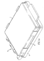
- Connector 10 has two matable pieces, a cassette 11 and a housing 13.
- Figure 1a displays cassette 11 and housing 13 in a mated condition
- Figure 1b displays an unmated condition.
- Cassette 11 and housing 13 will now be individually described.
- Figures 2a and 2b display cassette 11, preferably manufactured from a suitable plastic, such as a liquid crystal polymer (LCP).
- Cassette 11 can have a base 15, described throughout as a plate, that receives component 1.
- LCP liquid crystal polymer
- At least one aperture 17 extends through base 15.
- base 15 has a plurality of apertures 17.
- Apertures 17 are arranged on base plate 15 so as to receive corresponding pins 3 of electrical component 1. Thus, the arrangement of apertures 17 on base 15 is determined by the location of pins 3 on electrical component 1.
- apertures 17 could have beveled lead-ins to assist in the insertion of pins 3.
- pins 3 With electrical component 1 properly positioned on cassette 11, pins 3 extend past the lower surface of base plate 15 as seen in Figure 1b.
- Base plate 15 could include a wall 19 along its outer perimeter. As seen in the embodiment of Figure 2b, wall 19 extends below the lower surface of base plate 15, for example, to protect pins 3 from damage.
- Latches 21 extend from base plate 15, preferably along the sides.
- Latches 21 include a flange portion (see Figure 2a) projecting generally perpendicular from base plate 15.
- the distal ends of the flange portions include a retaining portion 23 extending from the flange portion.
- the area between retaining portion 23 and the upper surface of base plate 15 receives electrical component 1.
- Cassette 11 When properly seated within cassette 11, electrical component 1 can be mated with contacts 100.
- Cassette 11 rotates relative to housing 13 so that only a limited number of pins 3 mate with contacts 100 at one time.
- Cassette 11 rotates relative to housing 13 so that consecutive columns of pins 3 mate with consecutive columns of contacts 100.
- Wall 19 includes a tab 25 on a leading edge of base plate 15 to assist the installer in rotating cassette 11. The mating of pins 3 with contacts 100 will be described in greater detail below.
- Wall 19 also includes a hinge assembly 27 at a trailing edge of base plate 15.
- Hinge assembly 27, in conjunction with the hinge assembly on housing 13, allows rotation of cassette 11 relative to housing 13 and ensures the proper alignment of pins 3 of electrical component 1 with contacts 100 of housing 13 during the mating process.
- Hinge assembly 27 extends generally parallel to the plane of cassette 11. A description of the components of hinge assembly 27 follows.
- Extensions 29 project outwardly from the trailing edge of cassette 11, preferably at opposite sides of the trailing edge.
- Each extension 29 has a curved element 31 flanked by a pair of arms 33.
- Curved elements 31 have a first surface 67 shaped to engage a hinge pin on housing 13 and a second surface 69 opposite first surface 67 shaped to interact with a block 65 on housing 13.
- Each outermost arm 33 includes an outwardly facing, or exterior surface 35 that interacts with corresponding surfaces on the hinge assembly of housing 13 to ensure proper lateral alignment of pins 3 on electrical component 1 and the contacts on housing 13 during mating.
- Extension 39 projects outwardly from the trailing edge of housing 13.
- Extension 39 preferably extends from a central location along the trailing edge of housing 13 between extensions 29, but extends in a direction opposite of extensions 29.
- Central extension 39 has a curved element 71 flanked by a pair of arms 73. Curved elements 71 have a first surface 75 shaped to engage a hinge pin on housing 13 and a second surface 77 opposite first surface 75 and shaped to interact with block 65 on housing 13.
- Figures 3a and 3b display a portion of the lower surface of base plate 15.
- pins 3 of electrical component 1 can freely project from apertures 17 and extend beyond the bottom surface of base plate 15.
- Base plate 15 provides lateral support to the portions of pins 3 residing within base plate 15.
- the distal ends of pins 3 i.e. the portions of pins extending beyond the lower surface of base plate 15
- Figures 3c and 3d demonstrate an alternative arrangement in which base plate 15' laterally supports a greater length of pins 3' than the earlier alternative embodiment. Specifically, Figures 3c and 3d demonstrate an alternative arrangement of the lower surface of base plate 15', which includes bridges 79' positioned between each aperture 17'. Bridge 79' may include arcuate sides 81' and recessed ends 83'.
- Recessed ends 83' correspond to the shape of pins 3'. As seen in Figure 3c, if electrical component 1 uses round pins 3', recessed ends 83' have a rounded, concave shape to receive a portion of pin 3'.
- Bridges 79' are located on base plate 15' so as not to interfere with contacts 100'. As shown in Figure 3c, beams 101' of each contact 100' are arranged in a column, while bridges 79' are arranged in rows. Thus, the presence of bridges 79' do not affect the flexure of beams 101'. Bridges 79' may be molded unitarily with base plate 15'.
- Figures 4a-4c display housing 13, which is preferably manufactured from a suitable plastic.
- Housing 13 includes a base 41 with a plurality of apertures 43 extending therethrough.
- base 41 can have a generally planar configuration, although other orientations are possible.
- Each aperture 43 preferably includes three portions.
- First portion 45 is a relatively wide opening so as to accommodate the flexure of dual beams 101 of contact 100 during mating.
- Second portion 47 accommodates tail portion 103 of contact 100 and, as described below, a portion of a fusible element 105.
- third portion 49 retains intermediate portion 107 of contact 100 within aperture 43.
- beam accommodating portion 45 resides at the mating end of housing 13 and has tapered side walls 51 forming a lead-in. Tapered side walls 51 allow for the easy insertion of contact 100 within aperture 43 and allow the flexure of beams 101 by pins 3 without restriction.
- Tail accommodating portion 47 resides at the mounting end of housing 13. Since housing 13 can surface mount to substrate S, preferably using Ball Grid Array (BGA) technology, tail accommodating portion 47 can have a suitable shape to accommodate the BGA features.
- a fusible element such as a solder ball 105, secures to tail portion 103 of contact 100. At least a portion of solder ball 105 secured to tail portion 103 of contact 100 can seat within tail accommodating portion 47 of aperture 43.
- International Publication number WO 98/15989 International Application number PCT/US97/ 18066, herein incorporated by reference, describes methods of securing a solder ball to a contact and of securing a solder ball to a substrate.
- Intermediate portion 49 extends between beam accommodating portion 45 and tail accommodating portion 47.
- Opposed walls of intermediate portion 49 each include a protuberance 53 extending towards each other.
- protuberance 53 can be a rib extending axially along a length of aperture 43.
- the distance between opposed walls of intermediate portion 49 exceeds the width of contact 100 to allow contact 100 to pass through aperture 43.
- the width of contact 100 exceeds the distance between the opposed protuberances 53.
- contact 100 interference fits between protuberance 53 for retention in aperture 43.
- Base plate 41 can also have a wall 55 along its outer perimeter. Similar to wall 19 of cassette 11, wall 55 extends from plate 41 and protects contacts 100 from damage. When cassette 11 and housing 13 mate, wall 19 of cassette 11 resides between wall 55 and contacts 100. As seen in Figure 4a, the leading edge of wall 15 includes a notch 57 to receive tab 25 from cassette 11 when connector 10 is in a mated condition. This allows complete rotation of cassette 11 relative to housing 13 for mating all pins 3 and contacts 100. To avoid interference with hinge assemblies 27, 59, wall 55 is discontinuous in the trailing edge region of base 41.
- the trailing edge of base plate 41 includes a hinge assembly 59 that interacts with hinge assembly 27 of cassette 11 to allow rotation of cassette 11 relative to housing 13.
- Hinge assembly 59 extends generally parallel to the plane of housing 13 and includes a hinge pin 61 braced by a series of supports 63 along the trailing edge of housing 13.
- a series of cams, or blocks 65 extend from the trailing edge between adjacent supports 63.
- Blocks 65 have curved surfaces 75 that correspond to second surfaces 69, 77 of extensions 33 and central extension 35.
- Curved surfaces 75 of blocks 65 can be circular and preferably have substantially the same radius of curvature as second curved surfaces 69, 77 of extensions 33 and central extension 35. This can ensure proper longitudinal and Z-axis (i.e. normal to the plane of housing 13) alignment of pins 3 of electrical component 1 and contacts 100 in housing 13 for mating.
- Each outermost support 63 includes an inwardly facing, or interior surface 85 that interact with surfaces 35 of hinge assembly 27 to ensure proper alignment of pins 3 of electrical component E and contacts 100 during mating. Specifically, surfaces 35 of cassette 11 abut surfaces 85 of housing 13 for precisely aligning cassette 11 and housing 13 laterally for mating pins 3 and contacts 100.
- cassette 11 and housing 13 are separate, or unmated. In this condition, housing 13 should be secured to substrate S. As discussed above, housing 13 can be surface mounted to substrate S, preferably using BGA technology. However, other methods could be used.
- electrical component 1 secures to cassette 11.
- pins 3 of electrical component 1 enter apertures 17 until latch 21 retains electrical component 1 against cassette 11.
- hinge assemblies 27, 59 To interface cassette 11 and housing 13, hinge assemblies 27, 59 must mesh as shown in Figures 1b and 5. The features of hinge assemblies 27, 59, cassette 11 and housing 13 enhance the ease of blind mating cassette 11 and housing 13.
- extensions 29 and central extension 39 enter the openings formed between hinge pin 61, supports 63 and the trailing edge of housing 13. Insertion occurs in the direction designated by arrow A in Figure 5.
- Arms 33, 73 of hinge assembly 27 enter the areas flanking blocks 65 of hinge assembly 59.
- Outer surfaces 35 of arms 33 abut surfaces 85 of support 63. The interaction of outer surfaces 35 with inner surfaces 85 laterally align pins 3 and contacts 100 along an axis parallel to the trailing edges of cassette 11 and housing 13.
- surfaces 75 of blocks 65 begin to abut second surfaces 69, 77 of extensions 29 and central extension 39 as cassette 11 rotates along the direction of arrow B in Figure 5.
- Surfaces 69, 75, 77 help align cassette 11 and receptacle 13 along an axis parallel to the sides of cassette 11 and housing 13.
- the other adjacent surfaces of arms 33, supports 63 and blocks 65 have a clearance therebetween to reduce the amount of force required to rotate cassette 11.
- Extensions 29 and central extension 39 provide a retaining force on opposite sides of hinge pin 61 as seen in Figure 5 due to the opposite orientation of central element 39 relative to extensions 29.
- the retaining forces, along with the placing of extensions 29 and central extension 39 between hinge pin 61 and housing 13 prevents separation of cassette 11 from housing 13. In other words, cassette 11 can only separate from housing 13 by reversing the mating process (i.e. rotating cassette 11 away from housing 13).
- Rotation of cassette 11 relative to housing 13 begins the mating of pins 3 of electrical component 1 and contacts 100 in housing 13.
- the column of pins 3 and contacts 100 closest to the trailing edges of cassette 11 and housing 13 mate first. Mating progresses with each subsequent column away from the trailing edges of cassette 11 and housing 13. Sequential mating of pins 3 and contacts 100 reduces the peak insertion force when compared to ZIF sockets.
- cassette 11 begins the mating of pins 3 and contacts 100. Each pin 3 progressively enters the space between the opposite arms of the dual beam contacts during rotation.
- the dual beams retain pin 3.
- the area between the dual beams is oriented generally parallel to the mating axis of cassette 11 and housing 13.
- Figure 1a shows connector 10 in a fully mated and closed condition. While mated, wall 55 of housing 13 surrounds cassette 11 and tab 25 can enter recess 57 in the leading edge of housing 13.
Landscapes
- Engineering & Computer Science (AREA)
- Microelectronics & Electronic Packaging (AREA)
- Manufacturing & Machinery (AREA)
- Coupling Device And Connection With Printed Circuit (AREA)
- Connecting Device With Holders (AREA)
- Multi-Conductor Connections (AREA)
- Amplifiers (AREA)
- Organic Insulating Materials (AREA)
- Supply And Installment Of Electrical Components (AREA)
- Electric Connection Of Electric Components To Printed Circuits (AREA)
- Details Of Connecting Devices For Male And Female Coupling (AREA)
- Contacts (AREA)
Claims (25)
- Steckverbinder (10) für die elektrische Verbindung einer elektrischen Komponente (1), die mehrere von der Komponente abstehende leitende Elemente (3) aufweist, mit einem Substrat (S), der aufweist:eine erste Basis (15) für die Verbindung mit der elektrischen Komponente (1), die aufweist:mindestens eine Öffnung (17), die durch die Basis verläuft undzumindest einen Abschnitt der elektrischen Komponente (1) darin aufnehmen kann, undeine Gelenkanordnung (27), undeine zweite Basis (41), die an dem Substrat befestigt werden kann, und welche aufweist:mehrere Kontakte (100), die den leitenden Elementen (3) in der elektrischen Komponente (1) entsprechen, undeine Gelenkanordnung (39), die in die Gelenkanordnung (27) der ersten Basis (15) eingreifen kann und eine Rotationsbewegung der ersten Basis relativ zur zweiten Basis für ein Verbinden oder ein Lösen der leitenden Elemente (3) ermöglicht.
- Steckverbinder nach Anspruch 1, wobei die zumindest eine Öffnung (17) mehrere Öffnungen aufweist, wobei die erste Basis (15) eine Fläche aufweist, die der zweiten Basis (41) zugewandt ist und die mehrere Brücken aufweist, die sich zwischen benachbarten Öffnungen (17) erstrecken.
- Steckverbinder nach Anspruch 1, wobei die erste Basis (15) eine Struktur (21) für die Befestigung der elektrischen Komponente (1) an der ersten Basis aufweist.
- Steckverbinder nach Anspruch 3, wobei die Struktur eine Verriegelung (21) aufweist.
- Steckverbinder nach Anspruch 4, wobei die Verriegelung sich von einer Wand (19) erstreckt, die wenigstens teilweise um den Rand der ersten Basis (15) ausgebildet ist.
- Steckverbinder nach Anspruch 1, wobei die zumindest eine Öffnung (17) mehrere Öffnungen aufweist, die jeweils ein entsprechendes Element der leitenden Elemente (3) der elektrischen Komponente (1) aufnehmen können.
- Steckverbinder nach Anspruch 1, wobei die mehreren Kontakte (100) eine Reihe von Spalten bilden, die sich im wesentlichen parallel zur Gelenkanordnung (39) der zweiten Basis (41) erstrecken, wobei durch die Gelenkanordnungen (27, 39) die Spalten der Kontakte (100) nach und nach die leitenden Elemente (3) der elektrischen Komponente (1) treffen können.
- Steckverbinder nach Anspruch 1, wobei die Kontakte (100) zweischenklige Kontakte mit einem Kontaktraum zwischen den beiden Schenkeln und parallel zu den Gelenkanordnungen (27, 39) aufweisen.
- Steckverbinder nach Anspruch 1, der weiterhin mehrere schmelzbare Elemente (105) aufweist, die jeweils einzeln mit einem der vielen Kontakte (100) verbunden sind, um die zweite Basis (41) mit dem Substrat zu verbinden.
- Steckverbinder nach Anspruch 9, wobei die mehreren schmelzbaren Elemente (105) Lötkugeln sind.
- Steckverbinder nach Anspruch 1 in Verbindung mit einer elektrischen Komponente (1), die mehrere von ihr abstehende leitende Elemente (3) aufweist, wobei die elektrische Komponente (1) entfernbar in die Öffnung (17) in der Basis (15) einsetzbar ist und in mehrere Kontakte (100) in der zweiten Basis (41) eingreifen kann.
- Steckverbinder nach Anspruch 11, wobei die elektrische Komponente (1) eine Kontaktstiftreihenkomponente und ein Vielfach-Chipmodul ist.
- Steckverbinder nach Anspruch 12, wobei die elektrische Komponente einen IC-Chip aufweist.
- Kassette (11), die mit einem Gehäuse (13) für die Befestigung einer elektrischen Komponente auf einem Substrat zusammenwirken kann, welche aufweist:eine Basis (15),ein Gelenk (27) für eine Rotationsbewegung eines komplementären Gelenks des zusammenwirkenden Gehäuses, undmindestens eine Öffnung (17), die durch die Basis (15) verläuft und mindestens einen Abschnitt der elektrischen Komponente (1) aufnehmen kann.
- Kassette nach Anspruch 14, wobei die zumindest eine Öffnung (17) mehrere Öffnungen (17) aufweist, die jeweils ein entsprechendes leitendes Element (3) der elektrischen Komponente (1) aufnehmen können.
- Kassette nach Anspruch 15, wobei die Basis weiterhin mehrere Brücken aufweist, die zwischen benachbarten Öffnungen (17) verlaufen.
- Kassette nach Anspruch 14, die weiterhin eine Struktur für die Befestigung der elektrischen Komponente an der Kassette (11) aufweist.
- Kassette nach Anspruch 17, wobei die Struktur eine Verriegelung (21) aufweist.
- Kassette nach Anspruch 14 in Verbindung mit einer elektrischen Komponente (1), die mehrere von ihr abstehende leitende Elemente (3) aufweist, die mit mehreren Kontakten (100) in der zweiten Basis verbindbar sind.
- Kassette nach Anspruch 19, wobei die elektrische Komponente (1) eine Kontaktstiftreihenkomponente und ein Vielfach-Chipmodul ist.
- Kassette nach Anspruch 20, wobei die elektrische Komponente (1) einen IC-Chip aufweist.
- Gehäuse (13), das mit einer Kassette (11) für die Verbindung einer elektrischen Komponente (1), die mehrere von ihr abstehende leitende Elemente (3) aufweist, mit einem Substrat zusammenwirken kann, welches aufweist:eine Basis,ein Gelenk (27) für eine Rotationsbewegung mit einem komplementären Gelenk der zusammenwirkenden Kassette, undmehrere Kontakte in der Basis, die eine Reihe von Spalten bilden, die für die Aufnahme der leitenden Elemente (3) der elektrischen Komponente (1) angepaßt sind.
- Gehäuse (13) nach Anspruch 22, wobei die mehreren Kontakte zweischenklige Kontakte sind, die einen Kontaktraum aufweisen, der sich zwischen den beiden Schenkeln und parallel zum Gelenk erstreckt.
- Gehäuse (13) nach Anspruch 22, das weiterhin mehrere schmelzbare Elemente aufweist, die einzeln an einem jeweiligen elektrischen Kontakt (100) für die Befestigung des Gehäuses an dem Substrat befestigt sind.
- Gehäuse nach Anspruch 24, wobei die mehreren schmelzbaren Elemente Lötkugeln sind.
Priority Applications (3)
| Application Number | Priority Date | Filing Date | Title |
|---|---|---|---|
| EP01127319A EP1193800B1 (de) | 1998-12-18 | 1999-12-17 | Kontakt für elektrische Komponente |
| EP01127320A EP1193801B1 (de) | 1998-12-18 | 1999-12-17 | Befestigungsverfahren für eine elektrische Komponente |
| EP05020940.2A EP1624533B1 (de) | 1998-12-18 | 1999-12-17 | Kontakt für elektrische Komponente |
Applications Claiming Priority (2)
| Application Number | Priority Date | Filing Date | Title |
|---|---|---|---|
| US216574 | 1998-12-18 | ||
| US09/216,574 US6155860A (en) | 1998-01-31 | 1998-12-18 | Socket for electrical component |
Related Child Applications (3)
| Application Number | Title | Priority Date | Filing Date |
|---|---|---|---|
| EP01127319A Division EP1193800B1 (de) | 1998-12-18 | 1999-12-17 | Kontakt für elektrische Komponente |
| EP01127320A Division EP1193801B1 (de) | 1998-12-18 | 1999-12-17 | Befestigungsverfahren für eine elektrische Komponente |
| EP05020940.2A Division EP1624533B1 (de) | 1998-12-18 | 1999-12-17 | Kontakt für elektrische Komponente |
Publications (3)
| Publication Number | Publication Date |
|---|---|
| EP1014505A2 EP1014505A2 (de) | 2000-06-28 |
| EP1014505A3 EP1014505A3 (de) | 2000-11-08 |
| EP1014505B1 true EP1014505B1 (de) | 2003-04-02 |
Family
ID=22807614
Family Applications (4)
| Application Number | Title | Priority Date | Filing Date |
|---|---|---|---|
| EP01127320A Expired - Lifetime EP1193801B1 (de) | 1998-12-18 | 1999-12-17 | Befestigungsverfahren für eine elektrische Komponente |
| EP99125309A Expired - Lifetime EP1014505B1 (de) | 1998-12-18 | 1999-12-17 | Buchse für elektrische Komponente |
| EP05020940.2A Expired - Lifetime EP1624533B1 (de) | 1998-12-18 | 1999-12-17 | Kontakt für elektrische Komponente |
| EP01127319A Expired - Lifetime EP1193800B1 (de) | 1998-12-18 | 1999-12-17 | Kontakt für elektrische Komponente |
Family Applications Before (1)
| Application Number | Title | Priority Date | Filing Date |
|---|---|---|---|
| EP01127320A Expired - Lifetime EP1193801B1 (de) | 1998-12-18 | 1999-12-17 | Befestigungsverfahren für eine elektrische Komponente |
Family Applications After (2)
| Application Number | Title | Priority Date | Filing Date |
|---|---|---|---|
| EP05020940.2A Expired - Lifetime EP1624533B1 (de) | 1998-12-18 | 1999-12-17 | Kontakt für elektrische Komponente |
| EP01127319A Expired - Lifetime EP1193800B1 (de) | 1998-12-18 | 1999-12-17 | Kontakt für elektrische Komponente |
Country Status (11)
| Country | Link |
|---|---|
| US (2) | US6155860A (de) |
| EP (4) | EP1193801B1 (de) |
| JP (1) | JP2000188161A (de) |
| KR (1) | KR100609798B1 (de) |
| CN (3) | CN100365872C (de) |
| AT (3) | ATE236464T1 (de) |
| CA (1) | CA2291437A1 (de) |
| DE (3) | DE69930018T2 (de) |
| ES (1) | ES2193657T3 (de) |
| SG (1) | SG93221A1 (de) |
| TW (1) | TW519783B (de) |
Cited By (4)
| Publication number | Priority date | Publication date | Assignee | Title |
|---|---|---|---|---|
| US9455503B2 (en) | 2012-02-07 | 2016-09-27 | 3M Innovative Properties Company | Electrical connector contact terminal |
| US9509089B2 (en) | 2012-02-07 | 2016-11-29 | 3M Innovative Properties Company | Electrical connector latch |
| US9509094B2 (en) | 2012-02-07 | 2016-11-29 | 3M Innovative Properties Company | Board mount electrical connector with latch opening on bottom wall |
| US9553401B2 (en) | 2012-02-07 | 2017-01-24 | 3M Innovative Properties Company | Electrical connector for strain relief for an electrical cable |
Families Citing this family (40)
| Publication number | Priority date | Publication date | Assignee | Title |
|---|---|---|---|---|
| US6758702B2 (en) * | 2000-02-24 | 2004-07-06 | Fci Americas Technology, Inc. | Electrical connector with compression contacts |
| US6350141B1 (en) * | 2000-05-30 | 2002-02-26 | Fci Americas Technology, Inc. | Connector frame for a high density electrical connector |
| JP3469187B2 (ja) | 2000-09-29 | 2003-11-25 | タイコエレクトロニクスアンプ株式会社 | Icソケット |
| JP3537776B2 (ja) | 2001-02-22 | 2004-06-14 | 日本圧着端子製造株式会社 | ヒューズホルダー |
| JP2002251953A (ja) | 2001-02-22 | 2002-09-06 | Jst Mfg Co Ltd | マルチヒューズホルダー |
| JP2002251952A (ja) * | 2001-02-22 | 2002-09-06 | Jst Mfg Co Ltd | ヒューズホルダー |
| US6400577B1 (en) * | 2001-08-30 | 2002-06-04 | Tyco Electronics Corporation | Integrated circuit socket assembly having integral shielding members |
| US6488513B1 (en) | 2001-12-13 | 2002-12-03 | Intercon Systems, Inc. | Interposer assembly for soldered electrical connections |
| US6830463B2 (en) | 2002-01-29 | 2004-12-14 | Fci Americas Technology, Inc. | Ball grid array connection device |
| WO2003100792A2 (en) * | 2002-05-24 | 2003-12-04 | Molex Incorporated | Hinge connector for electronic devices |
| US6860741B2 (en) | 2002-07-30 | 2005-03-01 | Avx Corporation | Apparatus and methods for retaining and placing electrical components |
| US6928727B2 (en) * | 2002-07-30 | 2005-08-16 | Avx Corporation | Apparatus and method for making electrical connectors |
| US6851954B2 (en) | 2002-07-30 | 2005-02-08 | Avx Corporation | Electrical connectors and electrical components |
| US7008250B2 (en) * | 2002-08-30 | 2006-03-07 | Fci Americas Technology, Inc. | Connector receptacle having a short beam and long wipe dual beam contact |
| US6896539B2 (en) * | 2003-06-30 | 2005-05-24 | Hewlett-Packard Development Company, L.P. | Pivot component coupled with first circuit board for control of relative alignment of first circuit board connection component with second circuit board connection component |
| US7059873B2 (en) * | 2003-12-09 | 2006-06-13 | Fci Americas Technology, Inc. | LGA-BGA connector housing and contacts |
| US6979238B1 (en) * | 2004-06-28 | 2005-12-27 | Samtec, Inc. | Connector having improved contacts with fusible members |
| JP3143222U (ja) * | 2004-12-22 | 2008-07-17 | モレックス インコーポレーテッド | 改良されたデュアルビームコンタクトを備えたコネクタ |
| KR100630751B1 (ko) * | 2005-06-27 | 2006-10-02 | 삼성전자주식회사 | 커넥터 및 이를 구비한 하드디스크 드라이브 |
| US7097465B1 (en) * | 2005-10-14 | 2006-08-29 | Hon Hai Precision Ind. Co., Ltd. | High density connector with enhanced structure |
| US7422450B2 (en) * | 2006-09-15 | 2008-09-09 | Lotes Co., Ltd. | Electrical connector |
| CN200972994Y (zh) * | 2006-10-31 | 2007-11-07 | 富士康(昆山)电脑接插件有限公司 | 电连接器端子 |
| DE102008013199A1 (de) * | 2008-03-07 | 2009-09-17 | Beru Ag | Vorrichtung und Verfahren zur Erkennung von Fehlfunktionen bei Verbrennungsanomalien |
| CN201252216Y (zh) * | 2008-07-21 | 2009-06-03 | 富士康(昆山)电脑接插件有限公司 | 电连接器及其导电端子 |
| US7963790B1 (en) * | 2008-10-16 | 2011-06-21 | Winter John R Jr | Pivoting connector |
| TWM376962U (en) * | 2009-09-03 | 2010-03-21 | Hon Hai Prec Ind Co Ltd | Electrical connector and the contact |
| TWM382623U (en) * | 2009-12-18 | 2010-06-11 | Hon Hai Prec Ind Co Ltd | Electrical connector and contacts thereof |
| EP2339696A1 (de) * | 2009-12-22 | 2011-06-29 | General Electric Company | Elektrische Verbinderbaugruppe |
| US8052454B2 (en) * | 2009-12-31 | 2011-11-08 | Hon Hai Precision Ind. Co., Ltd. | Electrical connector with improved feature for securing solder ball thereon |
| US8105113B2 (en) * | 2010-04-21 | 2012-01-31 | Delphi Technologies, Inc. | Fuse adapter |
| CN101976778B (zh) * | 2010-10-20 | 2015-06-03 | 中兴通讯股份有限公司 | 一种对插座内的插针进行保护的装置 |
| FR2971891A1 (fr) * | 2011-02-22 | 2012-08-24 | Radiall Sa | Contact electrique pour connecteur |
| ES2388842B1 (es) | 2011-03-22 | 2013-06-12 | Construcciones Y Auxiliar De Ferrocarriles, S.A. | Sistema de carga eléctrica para acumuladores de energía de vehículos ferroviarios. |
| US8787035B2 (en) * | 2011-04-05 | 2014-07-22 | Tyco Electronics Corporation | Electrical interconnect device |
| JP5736262B2 (ja) * | 2011-07-14 | 2015-06-17 | モレックス インコーポレイテドMolex Incorporated | 多接点コネクタ |
| DE102011110184A1 (de) * | 2011-08-09 | 2013-02-14 | Pilz Gmbh & Co. Kg | Modulare Steuervorrichtung |
| CN104170172B (zh) | 2012-02-07 | 2017-06-09 | 3M创新有限公司 | 线材安装电连接器 |
| CN203250925U (zh) * | 2013-05-03 | 2013-10-23 | 泰科电子(上海)有限公司 | 连接器插头和连接器组件 |
| JP7365099B2 (ja) * | 2019-07-23 | 2023-10-19 | タイコエレクトロニクスジャパン合同会社 | インターポーザ |
| CN113937561B (zh) * | 2021-09-30 | 2024-05-14 | 中航光电科技股份有限公司 | 一种旋转接触电连接组件 |
Family Cites Families (37)
| Publication number | Priority date | Publication date | Assignee | Title |
|---|---|---|---|---|
| GB768242A (en) * | 1954-02-01 | 1957-02-13 | Edison Swan Electric Co Ltd | Improvements relating to the manufacture of electrical socket contacts |
| BE561443A (de) * | 1956-10-08 | |||
| DE1082645B (de) * | 1958-04-01 | 1960-06-02 | Harting Elektro W | Gabelfoermige Kontaktfeder |
| BE633052A (de) * | 1962-06-04 | |||
| US3865462A (en) * | 1973-03-07 | 1975-02-11 | Amp Inc | Preloaded contact and latchable housing assembly |
| NL174105C (nl) * | 1975-03-20 | 1984-04-16 | Philips Nv | Contactorgaan. |
| CA1096951A (en) * | 1978-02-03 | 1981-03-03 | Amp Incorporated | Polarised electrical connector |
| US4175821A (en) * | 1978-05-15 | 1979-11-27 | Teradyne, Inc. | Electrical connector |
| US4362353A (en) * | 1980-05-27 | 1982-12-07 | Amp Incorporated | Contact clip for connecting a ceramic substrate to a printed circuit board |
| US4396140A (en) | 1981-01-27 | 1983-08-02 | Bell Telephone Laboratories, Incorporated | Method of bonding electronic components |
| US4503608A (en) * | 1983-02-16 | 1985-03-12 | Elfab Corporation | Card edge connector tool and a method of joining a card edge connector |
| US4591230A (en) * | 1984-06-29 | 1986-05-27 | Frank Roldan | Electrical connector receptacle |
| US4761140A (en) * | 1987-02-20 | 1988-08-02 | Augat Inc. | Minimum insertion force self-cleaning anti-overstress PLCC receiving socket |
| US4869681A (en) * | 1987-08-28 | 1989-09-26 | Siemens Aktiengesellschaft | Front plug system with lagging end contact arrangement |
| JPH0625037Y2 (ja) * | 1987-12-11 | 1994-06-29 | ユニバーサル販売株式会社 | 回路基板取付構造 |
| US4836798A (en) * | 1987-12-21 | 1989-06-06 | Wells Electronics, Inc. | Zero insertion socket with normally closed contacts |
| US4887976A (en) * | 1988-08-18 | 1989-12-19 | Amp Incorporated | Electrical terminals for flat power cable |
| JPH0710496Y2 (ja) * | 1989-01-30 | 1995-03-08 | 日本航空電子工業株式会社 | Icパッケージ用コネクタ |
| US4988310A (en) * | 1989-10-10 | 1991-01-29 | Amp Incorporated | ZIF PGA socket and a tool for use therewith |
| US5057031A (en) * | 1990-08-15 | 1991-10-15 | Aries Electronics, Inc. | Zero insertion force pin grid array test socket |
| US5123855A (en) * | 1991-04-26 | 1992-06-23 | Minnesota Mining And Manufacturing Company | Zero insertion force connector for printed circuit boards |
| US5215472A (en) * | 1991-08-22 | 1993-06-01 | Augat Inc. | High density grid array socket |
| US5147213A (en) * | 1991-10-24 | 1992-09-15 | Minnesota Mining And Manufacturing Company | Zero insertion pressure test socket for pin grid array electronic packages |
| CN2150633Y (zh) * | 1992-08-04 | 1993-12-22 | 禾昌兴业股份有限公司 | 电路板连接器端子 |
| US5268820A (en) | 1992-08-18 | 1993-12-07 | Mitac International Corp. | Mother board assembly |
| US5302136A (en) * | 1992-11-23 | 1994-04-12 | Modicon, Inc. | Apparatus for positively preventing misengagement of multipoint connector elements |
| DE69423372T2 (de) * | 1993-01-06 | 2000-10-26 | Sumitomo Wiring Systems, Ltd. | Steckverbinder mit Verriegelungshebel |
| US5399108A (en) * | 1993-09-08 | 1995-03-21 | Tongrand Limited | LIF PGA socket and contact therein and method making the same |
| US5378169A (en) * | 1993-09-24 | 1995-01-03 | The Whitaker Corporation | Pivotal connector for planar electronic devices |
| US5762511A (en) * | 1994-10-11 | 1998-06-09 | Methode Eletronics, Inc. | Zero insertion force pin grid array socket |
| JP2747980B2 (ja) * | 1994-10-18 | 1998-05-06 | 日本航空電子工業株式会社 | 軸直角移動コネクタ |
| US5602719A (en) * | 1995-11-13 | 1997-02-11 | Intel Corporation | No handle zip socket |
| US5807142A (en) * | 1996-05-10 | 1998-09-15 | Molex Incorporated | Electrical connector having terminals with improved retention means |
| US5966023A (en) * | 1996-09-16 | 1999-10-12 | Virginia Panel Corporation | Rapid action engagement interface connection system |
| TW406454B (en) * | 1996-10-10 | 2000-09-21 | Berg Tech Inc | High density connector and method of manufacture |
| US6004142A (en) * | 1997-03-04 | 1999-12-21 | Micron Technology, Inc. | Interposer converter to allow single-sided contact to circuit modules |
| US5876219A (en) * | 1997-08-29 | 1999-03-02 | The Whitaker Corp. | Board-to-board connector assembly |
-
1998
- 1998-12-18 US US09/216,574 patent/US6155860A/en not_active Expired - Lifetime
-
1999
- 1999-12-01 SG SG9906079A patent/SG93221A1/en unknown
- 1999-12-02 CA CA002291437A patent/CA2291437A1/en not_active Abandoned
- 1999-12-13 TW TW088121791A patent/TW519783B/zh not_active IP Right Cessation
- 1999-12-15 JP JP11355926A patent/JP2000188161A/ja not_active Withdrawn
- 1999-12-17 ES ES99125309T patent/ES2193657T3/es not_active Expired - Lifetime
- 1999-12-17 DE DE69930018T patent/DE69930018T2/de not_active Expired - Fee Related
- 1999-12-17 KR KR1019990058461A patent/KR100609798B1/ko not_active Expired - Fee Related
- 1999-12-17 AT AT99125309T patent/ATE236464T1/de not_active IP Right Cessation
- 1999-12-17 CN CNB2003101205373A patent/CN100365872C/zh not_active Expired - Lifetime
- 1999-12-17 DE DE69930969T patent/DE69930969T2/de not_active Expired - Fee Related
- 1999-12-17 EP EP01127320A patent/EP1193801B1/de not_active Expired - Lifetime
- 1999-12-17 EP EP99125309A patent/EP1014505B1/de not_active Expired - Lifetime
- 1999-12-17 EP EP05020940.2A patent/EP1624533B1/de not_active Expired - Lifetime
- 1999-12-17 EP EP01127319A patent/EP1193800B1/de not_active Expired - Lifetime
- 1999-12-17 DE DE69906463T patent/DE69906463T2/de not_active Expired - Fee Related
- 1999-12-17 AT AT01127320T patent/ATE323957T1/de not_active IP Right Cessation
- 1999-12-17 CN CNB2003101205388A patent/CN100470940C/zh not_active Expired - Lifetime
- 1999-12-17 CN CNB991261941A patent/CN1136634C/zh not_active Expired - Lifetime
- 1999-12-17 AT AT01127319T patent/ATE319201T1/de not_active IP Right Cessation
-
2000
- 2000-09-29 US US09/675,218 patent/US6482050B1/en not_active Expired - Lifetime
Cited By (4)
| Publication number | Priority date | Publication date | Assignee | Title |
|---|---|---|---|---|
| US9455503B2 (en) | 2012-02-07 | 2016-09-27 | 3M Innovative Properties Company | Electrical connector contact terminal |
| US9509089B2 (en) | 2012-02-07 | 2016-11-29 | 3M Innovative Properties Company | Electrical connector latch |
| US9509094B2 (en) | 2012-02-07 | 2016-11-29 | 3M Innovative Properties Company | Board mount electrical connector with latch opening on bottom wall |
| US9553401B2 (en) | 2012-02-07 | 2017-01-24 | 3M Innovative Properties Company | Electrical connector for strain relief for an electrical cable |
Also Published As
| Publication number | Publication date |
|---|---|
| EP1193800A1 (de) | 2002-04-03 |
| EP1193800B1 (de) | 2006-03-01 |
| ES2193657T3 (es) | 2003-11-01 |
| ATE319201T1 (de) | 2006-03-15 |
| DE69930018D1 (de) | 2006-04-27 |
| JP2000188161A (ja) | 2000-07-04 |
| DE69906463T2 (de) | 2004-01-15 |
| EP1193801B1 (de) | 2006-04-19 |
| CN1510787A (zh) | 2004-07-07 |
| CA2291437A1 (en) | 2000-06-18 |
| CN100365872C (zh) | 2008-01-30 |
| CN1510786A (zh) | 2004-07-07 |
| DE69930969T2 (de) | 2006-12-21 |
| TW519783B (en) | 2003-02-01 |
| SG93221A1 (en) | 2002-12-17 |
| CN1136634C (zh) | 2004-01-28 |
| EP1193801A1 (de) | 2002-04-03 |
| ATE323957T1 (de) | 2006-05-15 |
| EP1014505A2 (de) | 2000-06-28 |
| EP1624533A1 (de) | 2006-02-08 |
| DE69906463D1 (de) | 2003-05-08 |
| KR100609798B1 (ko) | 2006-08-09 |
| EP1014505A3 (de) | 2000-11-08 |
| US6155860A (en) | 2000-12-05 |
| EP1624533B1 (de) | 2017-02-15 |
| CN1258117A (zh) | 2000-06-28 |
| KR20000048195A (en) | 2000-07-25 |
| DE69930018T2 (de) | 2006-10-12 |
| DE69930969D1 (de) | 2006-05-24 |
| ATE236464T1 (de) | 2003-04-15 |
| US6482050B1 (en) | 2002-11-19 |
| CN100470940C (zh) | 2009-03-18 |
Similar Documents
| Publication | Publication Date | Title |
|---|---|---|
| US6155860A (en) | Socket for electrical component | |
| EP0557898B1 (de) | Steckverbinder für die Kante einer gedruckten Schaltung | |
| US12051867B2 (en) | Card edge connector with a locking system | |
| US5383792A (en) | Insertable latch means for use in an electrical connector | |
| US6409525B1 (en) | Terminal position housing assembly | |
| EP0416322B1 (de) | Kontaktendstück in einem Schaltplattensockel | |
| EP1004152B1 (de) | Aufbau eines elektrischen steckverbinders | |
| WO1995022182A1 (en) | Electrical connector | |
| EP1128477B1 (de) | Elektrischer Verbinder mit Kompressionskontakten | |
| US10411378B2 (en) | Circuit card assemblies for a communication system | |
| US20210075178A1 (en) | Method of assembling contacts into housing via respective contact carriers discrete from one another | |
| JPH0677178U (ja) | ラッチ付き回路基板用電気コネクタ | |
| EP1104048A2 (de) | Elektrischer Verbinder mit Einsteckhilfe und mechanischer Unterstützungsanordnung | |
| KR20000022916A (ko) | Pga 패키지용의 점검 가능한 전기 커넥터 | |
| US6350141B1 (en) | Connector frame for a high density electrical connector | |
| US6093042A (en) | High density connector with low insertion force | |
| JP2002270312A (ja) | ボールが取着された挿入力零のソケット | |
| US5597318A (en) | ZIF for plastic chip carrier | |
| US11063391B2 (en) | Circuit card assemblies for a communication system | |
| TW202439703A (zh) | 用於具有高卡之系統之電連接器 | |
| US6422887B1 (en) | High durability, low mating force electrical connectors | |
| US20240006779A1 (en) | Direct Wire Contact | |
| CA2571599A1 (en) | Contact for electrical component socket | |
| US6406316B1 (en) | Electrical connector with multiple housings | |
| EP0510869B1 (de) | Elektrischer Verbinder mit Anschlüssen, welche mit dem Rand einer Leiterplatte zusammenwirken |
Legal Events
| Date | Code | Title | Description |
|---|---|---|---|
| PUAI | Public reference made under article 153(3) epc to a published international application that has entered the european phase |
Free format text: ORIGINAL CODE: 0009012 |
|
| AK | Designated contracting states |
Kind code of ref document: A2 Designated state(s): AT BE CH CY DE DK ES FI FR GB GR IE IT LI LU MC NL PT SE |
|
| AX | Request for extension of the european patent |
Free format text: AL;LT;LV;MK;RO;SI |
|
| PUAL | Search report despatched |
Free format text: ORIGINAL CODE: 0009013 |
|
| AK | Designated contracting states |
Kind code of ref document: A3 Designated state(s): AT BE CH CY DE DK ES FI FR GB GR IE IT LI LU MC NL PT SE |
|
| AX | Request for extension of the european patent |
Free format text: AL;LT;LV;MK;RO;SI |
|
| 17P | Request for examination filed |
Effective date: 20010308 |
|
| 17Q | First examination report despatched |
Effective date: 20010611 |
|
| AKX | Designation fees paid |
Free format text: AT BE CH CY DE DK ES FI FR GB GR IE IT LI LU MC NL PT SE |
|
| GRAH | Despatch of communication of intention to grant a patent |
Free format text: ORIGINAL CODE: EPIDOS IGRA |
|
| GRAH | Despatch of communication of intention to grant a patent |
Free format text: ORIGINAL CODE: EPIDOS IGRA |
|
| RAP1 | Party data changed (applicant data changed or rights of an application transferred) |
Owner name: FCI |
|
| GRAA | (expected) grant |
Free format text: ORIGINAL CODE: 0009210 |
|
| AK | Designated contracting states |
Designated state(s): AT BE CH CY DE DK ES FI FR GB GR IE IT LI LU MC NL PT SE |
|
| PG25 | Lapsed in a contracting state [announced via postgrant information from national office to epo] |
Ref country code: AT Free format text: LAPSE BECAUSE OF FAILURE TO SUBMIT A TRANSLATION OF THE DESCRIPTION OR TO PAY THE FEE WITHIN THE PRESCRIBED TIME-LIMIT Effective date: 20030402 |
|
| REG | Reference to a national code |
Ref country code: GB Ref legal event code: FG4D |
|
| REG | Reference to a national code |
Ref country code: CH Ref legal event code: EP |
|
| REG | Reference to a national code |
Ref country code: IE Ref legal event code: FG4D |
|
| REF | Corresponds to: |
Ref document number: 69906463 Country of ref document: DE Date of ref document: 20030508 Kind code of ref document: P |
|
| REG | Reference to a national code |
Ref country code: SE Ref legal event code: TRGR |
|
| REG | Reference to a national code |
Ref country code: CH Ref legal event code: NV Representative=s name: ROTTMANN, ZIMMERMANN + PARTNER AG |
|
| PG25 | Lapsed in a contracting state [announced via postgrant information from national office to epo] |
Ref country code: PT Free format text: LAPSE BECAUSE OF FAILURE TO SUBMIT A TRANSLATION OF THE DESCRIPTION OR TO PAY THE FEE WITHIN THE PRESCRIBED TIME-LIMIT Effective date: 20030702 Ref country code: GR Free format text: LAPSE BECAUSE OF FAILURE TO SUBMIT A TRANSLATION OF THE DESCRIPTION OR TO PAY THE FEE WITHIN THE PRESCRIBED TIME-LIMIT Effective date: 20030702 Ref country code: DK Free format text: LAPSE BECAUSE OF FAILURE TO SUBMIT A TRANSLATION OF THE DESCRIPTION OR TO PAY THE FEE WITHIN THE PRESCRIBED TIME-LIMIT Effective date: 20030702 |
|
| ET | Fr: translation filed | ||
| REG | Reference to a national code |
Ref country code: ES Ref legal event code: FG2A Ref document number: 2193657 Country of ref document: ES Kind code of ref document: T3 |
|
| PG25 | Lapsed in a contracting state [announced via postgrant information from national office to epo] |
Ref country code: LU Free format text: LAPSE BECAUSE OF NON-PAYMENT OF DUE FEES Effective date: 20031217 Ref country code: IE Free format text: LAPSE BECAUSE OF NON-PAYMENT OF DUE FEES Effective date: 20031217 Ref country code: CY Free format text: LAPSE BECAUSE OF FAILURE TO SUBMIT A TRANSLATION OF THE DESCRIPTION OR TO PAY THE FEE WITHIN THE PRESCRIBED TIME-LIMIT Effective date: 20031217 |
|
| PG25 | Lapsed in a contracting state [announced via postgrant information from national office to epo] |
Ref country code: MC Free format text: LAPSE BECAUSE OF NON-PAYMENT OF DUE FEES Effective date: 20031231 |
|
| PLBE | No opposition filed within time limit |
Free format text: ORIGINAL CODE: 0009261 |
|
| STAA | Information on the status of an ep patent application or granted ep patent |
Free format text: STATUS: NO OPPOSITION FILED WITHIN TIME LIMIT |
|
| 26N | No opposition filed |
Effective date: 20040105 |
|
| REG | Reference to a national code |
Ref country code: IE Ref legal event code: MM4A |
|
| PGFP | Annual fee paid to national office [announced via postgrant information from national office to epo] |
Ref country code: NL Payment date: 20071109 Year of fee payment: 9 Ref country code: ES Payment date: 20071211 Year of fee payment: 9 |
|
| PGFP | Annual fee paid to national office [announced via postgrant information from national office to epo] |
Ref country code: FI Payment date: 20071121 Year of fee payment: 9 Ref country code: CH Payment date: 20071009 Year of fee payment: 9 Ref country code: IT Payment date: 20071215 Year of fee payment: 9 |
|
| PGFP | Annual fee paid to national office [announced via postgrant information from national office to epo] |
Ref country code: BE Payment date: 20071221 Year of fee payment: 9 Ref country code: SE Payment date: 20071205 Year of fee payment: 9 |
|
| PGFP | Annual fee paid to national office [announced via postgrant information from national office to epo] |
Ref country code: GB Payment date: 20071106 Year of fee payment: 9 |
|
| PGFP | Annual fee paid to national office [announced via postgrant information from national office to epo] |
Ref country code: DE Payment date: 20071228 Year of fee payment: 9 |
|
| PGFP | Annual fee paid to national office [announced via postgrant information from national office to epo] |
Ref country code: FR Payment date: 20071204 Year of fee payment: 9 |
|
| BERE | Be: lapsed |
Owner name: *FCI Effective date: 20081231 |
|
| PG25 | Lapsed in a contracting state [announced via postgrant information from national office to epo] |
Ref country code: FI Free format text: LAPSE BECAUSE OF NON-PAYMENT OF DUE FEES Effective date: 20081217 |
|
| REG | Reference to a national code |
Ref country code: CH Ref legal event code: PL |
|
| EUG | Se: european patent has lapsed | ||
| GBPC | Gb: european patent ceased through non-payment of renewal fee |
Effective date: 20081217 |
|
| NLV4 | Nl: lapsed or anulled due to non-payment of the annual fee |
Effective date: 20090701 |
|
| PG25 | Lapsed in a contracting state [announced via postgrant information from national office to epo] |
Ref country code: BE Free format text: LAPSE BECAUSE OF NON-PAYMENT OF DUE FEES Effective date: 20081231 |
|
| REG | Reference to a national code |
Ref country code: FR Ref legal event code: ST Effective date: 20090831 |
|
| PG25 | Lapsed in a contracting state [announced via postgrant information from national office to epo] |
Ref country code: LI Free format text: LAPSE BECAUSE OF NON-PAYMENT OF DUE FEES Effective date: 20081231 Ref country code: DE Free format text: LAPSE BECAUSE OF NON-PAYMENT OF DUE FEES Effective date: 20090701 Ref country code: CH Free format text: LAPSE BECAUSE OF NON-PAYMENT OF DUE FEES Effective date: 20081231 |
|
| PG25 | Lapsed in a contracting state [announced via postgrant information from national office to epo] |
Ref country code: NL Free format text: LAPSE BECAUSE OF NON-PAYMENT OF DUE FEES Effective date: 20090701 Ref country code: GB Free format text: LAPSE BECAUSE OF NON-PAYMENT OF DUE FEES Effective date: 20081217 |
|
| REG | Reference to a national code |
Ref country code: ES Ref legal event code: FD2A Effective date: 20081218 |
|
| PG25 | Lapsed in a contracting state [announced via postgrant information from national office to epo] |
Ref country code: FR Free format text: LAPSE BECAUSE OF NON-PAYMENT OF DUE FEES Effective date: 20081231 Ref country code: ES Free format text: LAPSE BECAUSE OF NON-PAYMENT OF DUE FEES Effective date: 20081218 |
|
| PG25 | Lapsed in a contracting state [announced via postgrant information from national office to epo] |
Ref country code: SE Free format text: LAPSE BECAUSE OF NON-PAYMENT OF DUE FEES Effective date: 20081218 |
|
| PG25 | Lapsed in a contracting state [announced via postgrant information from national office to epo] |
Ref country code: IT Free format text: LAPSE BECAUSE OF NON-PAYMENT OF DUE FEES Effective date: 20081217 |