EP1016206B1 - Steuerschaltung und -verfahren für einen piezoelektrischen transformator - Google Patents
Steuerschaltung und -verfahren für einen piezoelektrischen transformator Download PDFInfo
- Publication number
- EP1016206B1 EP1016206B1 EP98901085A EP98901085A EP1016206B1 EP 1016206 B1 EP1016206 B1 EP 1016206B1 EP 98901085 A EP98901085 A EP 98901085A EP 98901085 A EP98901085 A EP 98901085A EP 1016206 B1 EP1016206 B1 EP 1016206B1
- Authority
- EP
- European Patent Office
- Prior art keywords
- circuit
- voltage
- driving
- piezoelectric transformer
- oscillation
- Prior art date
- Legal status (The legal status is an assumption and is not a legal conclusion. Google has not performed a legal analysis and makes no representation as to the accuracy of the status listed.)
- Expired - Lifetime
Links
- 238000000034 method Methods 0.000 title claims description 8
- 230000010355 oscillation Effects 0.000 claims abstract description 134
- 238000001514 detection method Methods 0.000 claims abstract description 28
- 230000001954 sterilising effect Effects 0.000 claims description 5
- 230000004044 response Effects 0.000 claims description 4
- 238000004659 sterilization and disinfection Methods 0.000 claims description 3
- CBENFWSGALASAD-UHFFFAOYSA-N Ozone Chemical compound [O-][O+]=O CBENFWSGALASAD-UHFFFAOYSA-N 0.000 claims description 2
- 239000003054 catalyst Substances 0.000 claims description 2
- 230000001877 deodorizing effect Effects 0.000 claims description 2
- 238000000746 purification Methods 0.000 claims description 2
- XLYOFNOQVPJJNP-UHFFFAOYSA-N water Substances O XLYOFNOQVPJJNP-UHFFFAOYSA-N 0.000 claims description 2
- 238000005070 sampling Methods 0.000 claims 4
- 230000007423 decrease Effects 0.000 abstract description 15
- 238000010586 diagram Methods 0.000 description 10
- 230000004048 modification Effects 0.000 description 10
- 238000012986 modification Methods 0.000 description 10
- 239000000872 buffer Substances 0.000 description 5
- 239000003990 capacitor Substances 0.000 description 5
- 238000004804 winding Methods 0.000 description 5
- 230000000052 comparative effect Effects 0.000 description 4
- 230000001276 controlling effect Effects 0.000 description 4
- 239000004973 liquid crystal related substance Substances 0.000 description 4
- 230000008859 change Effects 0.000 description 3
- 238000006243 chemical reaction Methods 0.000 description 3
- 230000005669 field effect Effects 0.000 description 3
- 230000004913 activation Effects 0.000 description 1
- 239000000919 ceramic Substances 0.000 description 1
- 230000003247 decreasing effect Effects 0.000 description 1
- 230000000694 effects Effects 0.000 description 1
- 230000001939 inductive effect Effects 0.000 description 1
- 230000001105 regulatory effect Effects 0.000 description 1
Images






Classifications
-
- H—ELECTRICITY
- H02—GENERATION; CONVERSION OR DISTRIBUTION OF ELECTRIC POWER
- H02M—APPARATUS FOR CONVERSION BETWEEN AC AND AC, BETWEEN AC AND DC, OR BETWEEN DC AND DC, AND FOR USE WITH MAINS OR SIMILAR POWER SUPPLY SYSTEMS; CONVERSION OF DC OR AC INPUT POWER INTO SURGE OUTPUT POWER; CONTROL OR REGULATION THEREOF
- H02M5/00—Conversion of AC power input into AC power output, e.g. for change of voltage, for change of frequency, for change of number of phases
- H02M5/40—Conversion of AC power input into AC power output, e.g. for change of voltage, for change of frequency, for change of number of phases with intermediate conversion into DC
- H02M5/42—Conversion of AC power input into AC power output, e.g. for change of voltage, for change of frequency, for change of number of phases with intermediate conversion into DC by static converters
- H02M5/44—Conversion of AC power input into AC power output, e.g. for change of voltage, for change of frequency, for change of number of phases with intermediate conversion into DC by static converters using discharge tubes or semiconductor devices to convert the intermediate DC into AC
-
- H—ELECTRICITY
- H02—GENERATION; CONVERSION OR DISTRIBUTION OF ELECTRIC POWER
- H02M—APPARATUS FOR CONVERSION BETWEEN AC AND AC, BETWEEN AC AND DC, OR BETWEEN DC AND DC, AND FOR USE WITH MAINS OR SIMILAR POWER SUPPLY SYSTEMS; CONVERSION OF DC OR AC INPUT POWER INTO SURGE OUTPUT POWER; CONTROL OR REGULATION THEREOF
- H02M7/00—Conversion of AC power input into DC power output; Conversion of DC power input into AC power output
- H02M7/42—Conversion of DC power input into AC power output without possibility of reversal
- H02M7/44—Conversion of DC power input into AC power output without possibility of reversal by static converters
- H02M7/48—Conversion of DC power input into AC power output without possibility of reversal by static converters using discharge tubes with control electrode or semiconductor devices with control electrode
- H02M7/53—Conversion of DC power input into AC power output without possibility of reversal by static converters using discharge tubes with control electrode or semiconductor devices with control electrode using devices of a triode or transistor type requiring continuous application of a control signal
- H02M7/537—Conversion of DC power input into AC power output without possibility of reversal by static converters using discharge tubes with control electrode or semiconductor devices with control electrode using devices of a triode or transistor type requiring continuous application of a control signal using semiconductor devices only, e.g. single switched pulse inverters
- H02M7/538—Conversion of DC power input into AC power output without possibility of reversal by static converters using discharge tubes with control electrode or semiconductor devices with control electrode using devices of a triode or transistor type requiring continuous application of a control signal using semiconductor devices only, e.g. single switched pulse inverters in a push-pull configuration
-
- H—ELECTRICITY
- H05—ELECTRIC TECHNIQUES NOT OTHERWISE PROVIDED FOR
- H05B—ELECTRIC HEATING; ELECTRIC LIGHT SOURCES NOT OTHERWISE PROVIDED FOR; CIRCUIT ARRANGEMENTS FOR ELECTRIC LIGHT SOURCES, IN GENERAL
- H05B41/00—Circuit arrangements or apparatus for igniting or operating discharge lamps
- H05B41/14—Circuit arrangements
- H05B41/26—Circuit arrangements in which the lamp is fed by power derived from DC by means of a converter, e.g. by high-voltage DC
- H05B41/28—Circuit arrangements in which the lamp is fed by power derived from DC by means of a converter, e.g. by high-voltage DC using static converters
- H05B41/282—Circuit arrangements in which the lamp is fed by power derived from DC by means of a converter, e.g. by high-voltage DC using static converters with semiconductor devices
- H05B41/2821—Circuit arrangements in which the lamp is fed by power derived from DC by means of a converter, e.g. by high-voltage DC using static converters with semiconductor devices by means of a single-switch converter or a parallel push-pull converter in the final stage
- H05B41/2822—Circuit arrangements in which the lamp is fed by power derived from DC by means of a converter, e.g. by high-voltage DC using static converters with semiconductor devices by means of a single-switch converter or a parallel push-pull converter in the final stage using specially adapted components in the load circuit, e.g. feed-back transformers, piezoelectric transformers; using specially adapted load circuit configurations
-
- H—ELECTRICITY
- H05—ELECTRIC TECHNIQUES NOT OTHERWISE PROVIDED FOR
- H05B—ELECTRIC HEATING; ELECTRIC LIGHT SOURCES NOT OTHERWISE PROVIDED FOR; CIRCUIT ARRANGEMENTS FOR ELECTRIC LIGHT SOURCES, IN GENERAL
- H05B41/00—Circuit arrangements or apparatus for igniting or operating discharge lamps
- H05B41/14—Circuit arrangements
- H05B41/36—Controlling
- H05B41/38—Controlling the intensity of light
- H05B41/39—Controlling the intensity of light continuously
- H05B41/392—Controlling the intensity of light continuously using semiconductor devices, e.g. thyristor
- H05B41/3921—Controlling the intensity of light continuously using semiconductor devices, e.g. thyristor with possibility of light intensity variations
- H05B41/3925—Controlling the intensity of light continuously using semiconductor devices, e.g. thyristor with possibility of light intensity variations by frequency variation
-
- C—CHEMISTRY; METALLURGY
- C02—TREATMENT OF WATER, WASTE WATER, SEWAGE, OR SLUDGE
- C02F—TREATMENT OF WATER, WASTE WATER, SEWAGE, OR SLUDGE
- C02F1/00—Treatment of water, waste water, or sewage
- C02F1/30—Treatment of water, waste water, or sewage by irradiation
- C02F1/32—Treatment of water, waste water, or sewage by irradiation with ultraviolet light
Definitions
- the present invention relates to a control circuit and method for a piezoelectric transformer suited for use in a driving apparatus for a cold-cathode fluorescent lamp (CCFL).
- CCFL cold-cathode fluorescent lamp
- liquid crystal displays are extensively used as display devices of, e.g., portable notebook personal computers.
- These liquid crystal display devices incorporate a cold-cathode fluorescent lamp as a so-called back light in order to illuminate a liquid crystal display panel from the back.
- a cold-cathode fluorescent lamp requires an inverter capable of converting a low DC voltage of a battery or the like into a high AC voltage of 1,000 Vrms or more in an initial lighting state and about 500 Vrms in a steady lighting state.
- a winding transformer is used as a boosting transformer of this inverter.
- a piezoelectric transformer which performs electric conversion via mechanical energy and thereby performs boosting is beginning to be used.
- This piezoelectric transformer has a generally unpreferable characteristic, i.e., largely changes its boosting ratio in accordance with the magnitude of an output load (load resistance).
- this dependence upon a load resistance is suited to the characteristics of an inverter power supply for a cold-cathode fluorescent lamp. Accordingly, a piezoelectric transformer has attracted attention as a small-sized, high-voltage power supply meeting the demands for a low profile and a high efficiency of a liquid crystal display.
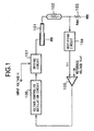
- An example of a control circuit for this piezoelectric transformer will be described below with reference to Fig. 1.
- Fig. 1 is a block diagram of a piezoelectric transformer control circuit as the prior art.
- reference numeral 101 denotes a piezoelectric transformer
- 102 a load such as a cold-cathode fluorescent lamp connected to the output terminal of the piezoelectric transformer 101
- 103 a detecting resistor Rdet for detecting a current flowing in the load
- 104 a rectifying circuit for converting an AC voltage generated in the detecting resistor 103 into a DC voltage
- 105 an error amplifier for comparing a voltage (to be referred to as a load current detection voltage hereinafter) Vri rectified by the rectifying circuit 104 with a reference voltage Vref and amplifying the difference as a comparison result
- 106 a voltage-controlled oscillation circuit for outputting a signal having an oscillation frequency (to be referred to as an oscillation signal hereinafter) in accordance with the output voltage from the error amplifier 105
- 107 a driving circuit for driving the piezoelectric transformer 101 on the basis of the oscillation signal from the voltage-controlled oscillation circuit 106, and an input
- Fig. 2 is a view showing an example of the internal arrangement of the driving circuit as the prior art.
- reference numeral 107a denotes a transistor such as a FET (Field Effect Transistor) for generating an AC voltage by switching the input voltage Vi in accordance with an oscillation signal from the voltage-controlled oscillation circuit 106; and 107b, a winding transformer for applying the AC voltage to the piezoelectric transformer 101. Since the winding transformer 107b has a filter effect by a secondary inductive component and a capacitive component of the piezoelectric transformer 101, a rectangular-wave voltage generated by switching of the transistor 107a is changed into a sine wave on the secondary side of the winding transformer 107b to be applied to the piezoelectric transformer. This sine-wave voltage drives the piezoelectric transformer 101 to generate a high AC voltage at the output terminal of the piezoelectric transformer 101.
- FET Field Effect Transistor
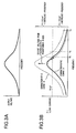
- Figs. 3A and 3B are graphs for explaining an example of frequency characteristics for an output voltage from the piezoelectric transformer and a load current.
- the piezoelectric transformer 101 has a hilly resonance frequency characteristic whose peak is the resonance frequency of the piezoelectric transformer 101. It is generally known that a current flowing in the load 102 due to the output voltage from the piezoelectric transformer 101 also has a similar hilly characteristic. In Fig. 3B, this load current is represented by the load current detection voltage Vri (characteristic curve A). Control using a right-side (falling) portion in this characteristic will be described below. When the power supply of this control circuit is turned on, the voltage-controlled oscillation circuit 106 starts oscillating at an initial frequency fa. Since no current flows in the load 102 at that time, the voltage generated in the detecting resistor 103 is zero.
- the error amplifier 105 outputs a negative voltage, as a result of comparison of the load current detection voltage Vri with the reference voltage Vref, to the voltage-controlled oscillation circuit 106.
- the voltage-controlled oscillation circuit 106 shifts the oscillation frequency of an oscillation signal to a lower frequency. Therefore, as the frequency is shifted to a lower frequency, the output voltage from the piezoelectric transformer 101 rises, and the load current (load current detection voltage Vri) also increases.
- the frequency stabilizes (fb).
- the oscillation frequency of the voltage-controlled oscillation circuit 106 shifts in response to the change to always hold the load current substantially constant.
- the input/output conversion efficiency of the piezoelectric transformer is the highest when the piezoelectric transformer is driven at a frequency around the resonance frequency of the piezoelectric transformer, and lowers as the frequency shifts to a higher frequency. Therefore, although the control circuit has a desirable function of holding the load current at a predetermined value even if the input voltage Vi changes, the driving frequency of the piezoelectric transformer varies owing to variations in input voltage Vi, resulting in a low conversion efficiency.
- Document US-A-5 424 935 describes a power convertor wherein a piezoelectric ceramic transformer generates a voltage, a resulting current passes through a load and a comparative voltage generator to generate a comparative voltage.
- the comparative voltage is amplified by a comparative voltage amplifying circuit and compared to a standard voltage, outputted by a standard voltage generating circuit, to obtain a control voltage.
- the control voltage is regulated by a voltage regulator to provide base potentials of the current amplifier connected to a driving coil.
- a piezoelectric transformer control circuit of the present invention has the following arrangements.
- a piezoelectric transformer control circuit for switching an input DC voltage by a driving circuit to generate an AC voltage, and driving a piezoelectric transformer by the AC voltage to obtain a high AC voltage, comprises a driving voltage detecting circuit for detecting a magnitude of a driving voltage to the piezoelectric transformer; a driving voltage error output circuit for comparing an output from the driving voltage detecting circuit with a first predetermined value and outputting a voltage error result as an amplified comparison difference; a load current detecting circuit for detecting a magnitude of a current flowing in a load connected to the piezoelectric transformer; a load current error output circuit for comparing an output from the load current detecting circuit with a second predetermined value and outputting a current error result as an amplified comparison differnce; and an oscillating circuit for outputting an oscillation signal for switching the input voltage.
- the oscillation signal is a rectangular wave
- the oscillating circuit includes a frequency adjusting circuit for adjusting a frequency of the oscillation signal in accordance with the current error result, and a duty ratio adjusting circuit for adjusting a duty ratio of the oscillation signal, which is outputted from the frequency adjusting circuit, in accordance with the output from the voltage error result.
- the load current is controlled to the second predetermined value, and the driving voltage to the piezoelectric transformer is controlled as to the predetermined value regardless of changes in input voltage.
- a piezoelectric transformer control method of the present invention has the following arrangements.
- a piezoelectric transformer control method of switching an input DC voltage to generate an AC voltage, and driving a piezoelectric transformer by the AC voltage to obtain a high AC voltage comprises a driving voltage detection step of detecting a magnitude of a driving voltage to the piezoelectric transformer; a first comparison step of comparing the detected driving voltage with a first predetermined value and amplifying a first comparison result; a load current detection step of detecting a magnitude of a current flowing in a load connected to the piezoelectric transformer; a second comparison step of comparing the detected load current with a second predetermined value and amplifying a second comparison result; and an oscillation step of generating an oscillation signal for switching the input voltage; wherein the oscillation signal is a rectangular wave and the oscillation step comprises a frequency adjustment step of adjusting a frequency of the oscillation signal in accordance with the first amplified comparison result in the first comparison step; and a duty ratio adjustment step of adjusting a duty ratio of the oscillation signal adjusted in the frequency adjustment step in accordance
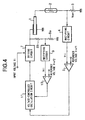
- Fig. 4 is a block diagram of a piezoelectric transformer control circuit as the first embodiment of the present invention.
- reference numeral 1 denotes a piezoelectric transformer
- a load such as a cold-cathode fluorescent lamp connected to the output terminal of the piezoelectric transformer 1
- a detecting resistor Rdet for detecting a current flowing in the load
- a rectifying circuit for converting an AC voltage generated in the detecting resistor 3 into a DC voltage
- an error amplifier for- comparing an output voltage (load current detection voltage) Vri from the rectifying circuit 4 with a reference voltage Vref1 and amplifying the difference
- 7, a driving circuit having the same arrangement as that in Fig.
- 8a and 8b detecting resistors for detecting the magnitude of a driving voltage to the piezoelectric transformer 1; 9, a rectifying circuit for converting an AC voltage generated in the detecting resistor 8a into a DC voltage; 10, an error amplifier for comparing an output voltage Vti from the rectifying circuit 9 with a reference voltage Vref2 and amplifying the difference; and 11, a voltage-controlled oscillation circuit for outputting an oscillation signal having a frequency corresponding to an output voltage from the error amplifier 5, and a duty ratio corresponding to an output voltage from the error amplifier 10.
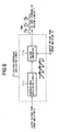
- Fig. 5 is a view showing the internal arrangement of the voltage-controlled oscillation circuit as the first embodiment of the present invention.
- the voltage-controlled oscillation circuit 11 comprises a triangular-wave oscillation circuit 11a and a voltage comparator 11b.
- the triangular-wave oscillation circuit 11a outputs, as an oscillation signal, a triangular wave having a frequency corresponding to an output voltage from the error amplifier 5.
- the voltage comparator 11b performs so-called PWM (Pulse Width Modulation) on the basis of the comparison result of the triangular wave output from the triangular-wave oscillation circuit 11a and an output voltage from the error amplifier 10, and outputs a rectangular wave. As the voltage of the error amplifier 10 rises, an oscillation signal having a smaller duty ratio is output to the driving circuit 7.
- PWM Pulse Width Modulation
- the driving circuit 7 drives the piezoelectric transformer 1 on the basis of the oscillation signal with a duty ratio of 40%.
- the input voltage Vi rises to 7 V in this state.
- the rise in input voltage Vi increases (the amplitude of) a sine-wave voltage for driving the piezoelectric transformer 1, and also increases the detection voltage Vti obtained by the driving voltage detecting resistors 8a and 8b, which are connected to the input terminal of the piezoelectric transformer 1, and the rectifying circuit 9.
- an output voltage from the error amplifier 10 rises, and the voltage-controlled oscillation circuit 11 operates to decrease the duty ratio of the oscillation signal.
- the duty ratio of the oscillation signal decreases, the duty ratio of a rectangular-wave voltage generated by switching of the transistor 107a also decreases.
- the voltage-controlled oscillation circuit 11 operates to decrease the driving voltage to the piezoelectric transformer 1.
- the duty ratio is increased to increase the driving voltage to the piezoelectric transformer 1.
- Fig. 6 is a view showing the internal arrangement of the voltage-controlled oscillation circuit as a modification of the first embodiment of the present invention.
- the voltage-controlled oscillation circuit comprises a sawtooth-wave oscillation circuit 11c for outputting a sawtooth wave having a frequency corresponding to an output voltage from the error amplifier 5, and a voltage comparator 11b for performing so-called PWM (Pulse Width Modulation) on the basis of the comparison result of the sawtooth wave output from the sawtooth-wave oscillation circuit 11c and an output voltage from the error amplifier 10 and outputting a rectangular wave.
- PWM Pulse Width Modulation
- a driving circuit 7 is of a so-called half-bridge or full-bridge type using a switching transistor will be described as the second embodiment. Since a half-bridge or full-bridge circuit arrangement is general, a detailed description thereof will be omitted. Figs. 7 and 8 schematically show the driving circuit.
- Fig. 7 is a view showing the internal arrangement of the half-bridge type driving circuit as the second embodiment of the present invention.
- transistors 7a and 7b such as FETs (Field Effect Transistors; in the second embodiment, the transistors 7a and 7b are of the p- and n-type, respectively) are constituted into a half-bridge form, as shown in Fig. 7.
- Two types of oscillation signals are respectively input from a voltage-controlled oscillation circuit 11A (to be described later) to high and low sides to alternately turn on/off the transistors 7a and 7b.
- the input voltage Vi is converted into a rectangular wave having a peak value Vi corresponding to an oscillation signal.
- a harmonic component is removed from this rectangular wave by a choke coil 10a, and the obtained wave serves as a sine-wave driving voltage to a piezoelectric transformer 1.
- Fig. 8 is a view showing the internal arrangement of a full-bridge type driving circuit as the second embodiment of the present invention.
- transistors 7a to 7d such as FETs (Field Effect Transistors; in the second embodiment, the transistors 7a and 7c are of the p-type, and the transistors 7b and 7d are of the n-type) are constituted into a full-bridge form, as shown in Fig. 8.
- Reference numeral 12 denotes a NOT circuit for reversing an oscillation signal; and 10b and 10c, choke coils. Switching of the full-bridge type driving circuit 7B is performed by respectively inputting two types of oscillation signals from the voltage-controlled oscillation circuit 11A (to be described later) to high and low sides and alternately turning on/off the transistors 7a and 7c and the transistors 7b and 7d.
- the input voltage Vi is converted into a rectangular wave having a peak value Vi corresponding to an oscillation signal by the switching operation of the driving circuit 7B, and this rectangular wave is converted into a sine wave by choke coils 10b and 10c.
- This is the same as in the half-bridge type driving circuit though the driving voltage of the full-bridge type driving circuit is naturally twice the driving voltage of the half-bridge type driving circuit owing to the full-bridge circuit arrangement.
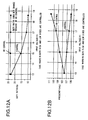
- Figs. 12A and 12B show circuit characteristics obtained when the duty ratios of high- and low-side oscillation signals are controlled, i.e., when a common oscillation signal having undergone pulse width modulation is input to the high and low sides from the voltage-controlled oscillation circuit 11 in Fig. 5 described above.
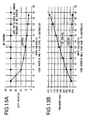
- Figs. 13A and 13B show circuit characteristics obtained when the duty ratio of only a high-side oscillation signal is controlled.
- control pulse width modulation
- Fig. 9 is a view showing the internal arrangement of the voltage-controlled oscillation circuit as the second embodiment of the present invention.
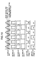
- Fig. 10 is a timing chart for explaining the operation of the voltage-controlled oscillation circuit as the second embodiment of the present invention.
- the voltage-controlled oscillation circuit 11A comprises a triangular-wave generation circuit 11a, voltage comparators 11ba and 11bb, a 1/2-frequency-dividing circuit 11d, and AND circuits 11e and 11f.
- the triangular-wave generation circuit 11a outputs a triangular wave having a frequency corresponding to an output signal from an error amplifier 5.
- the voltage comparator 11ba performs so-called pulse width modulation (PWM) on the basis of the comparison result of the triangular wave output from the triangular-wave generation circuit 11a and an output voltage from an error amplifier 10, and outputs a rectangular wave A.
- the voltage comparator 11bb outputs a rectangular wave B on the basis of the comparison result of the triangular wave output from the triangular-wave generation circuit 11a and an internal reference voltage as a predetermined value.
- the 1/2-frequency-dividing circuit 11d reverses its output at the leading edge of the rectangular wave B output from the voltage comparator 11bb to output a rectangular wave C having a frequency 1/2 the frequency of the rectangular wave B.
- the AND circuit 11e outputs a reversed output of the AND between the rectangular wave A and the reversed output of the rectangular wave C (high-side oscillation signal 1).
- the AND circuit 11f outputs the AND between the rectangular waves B and C (low-side oscillation signal 2). With this circuit arrangement, the duty ratio of only high-side oscillation signal 1 can be controlled in accordance with an output voltage from the error amplifier 10.
- Fig. 11 is a view showing the internal arrangement of a voltage-controlled oscillation circuit as a modification of the second embodiment of the present invention.
- the voltage-controlled oscillation circuit comprises a sawtooth-wave generation circuit 11c for generating a sawtooth wave, instead of the triangular-wave generation circuit 11a.
- the remaining arrangement and operation are substantially the same as in Fig. 9, and a description thereof will be omitted.
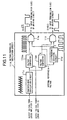
- the third embodiment will exemplify the case wherein a wide-range brightness control function for a cold-cathode fluorescent lamp serving as a load 2 is added to the piezoelectric transformer control circuit described in the first embodiment.
- Fig. 15 is a block diagram of a piezoelectric transformer control circuit as the third embodiment of the present invention.
- the same references as in the control circuit of Fig. 4 described in the first embodiment denote the same parts in Fig. 15, and a description thereof will be omitted.
- reference numeral 13 denotes a pulse power supply circuit for generating, from the input voltage Vi, a pulse-like power supply voltage (to be referred to as a pulse voltage hereinafter) to be supplied to a driving circuit 7, and controlling the pulse width or interval of the pulse voltage.
- the driving circuit 7 intermittently outputs a driving voltage for driving a piezoelectric transformer from the pulse voltage of the pulse power supply circuit 13.
- the piezoelectric transformer 1 is driven by the intermittent driving voltage, and as a result, an intermittent high voltage is generated at the output terminal of the piezoelectric transformer 1. If the pulse width or interval of the pulse voltage to be supplied to the driving circuit 7 is changed in the pulse power supply circuit 13 at this time, the ratio of the lighting period to the non-lighting period of the cold-cathode fluorescent lamp serving as the load 2 can be changed to realize a wide-range brightness control function for the cold-cathode fluorescent lamp.
- the luminance cannot be changed only by adding the pulse power supply circuit 13 to the control circuit in Fig. 4, and supplying the pulse voltage generated by the circuit 13 to the driving circuit 7.
- the control circuit in Fig. 4 comprises the "function of controlling a load current to a substantially predetermined value" by the error amplifier 5 and the like, and the “function of controlling a piezoelectric transformer driving voltage to a predetermined value regardless of changes in input voltage” by the error amplifier 10 and the like, as described above. The reason will be described below.
- a sample-and-hold circuit 14 is inserted between a rectifying circuit 4 and an error amplifier 5, whereas a sample-and-hold circuit 15 is inserted between a rectifying circuit 9 and an error amplifier 10, as shown in Fig. 15.
- Both the sample-and-hold circuits 14 and 15 are controlled by a pulse voltage output from the pulse power supply circuit 13.
- the sample-and-hold circuits 14 and 15 are respectively constituted by buffers 14a and 15a, charging capacitors 14b and 15b, and switching elements 14c and 15c.
- a pulse voltage to be output is adjusted to a continuous DC voltage by an adjusting means (not shown) of the pulse power supply circuit 13.
- the switching elements 14c and 15c are kept closed in the sample-and-hold circuits 14 and 15. This is equivalent to Fig. 4 wherein the control circuit has no sample-and-hold circuit 14 or 15.
- the state of the pulse voltage to be output is adjusted from the continuous DC voltage to a pulse-like voltage (pulse voltage) by the adjusting means (not shown) of the pulse power supply circuit 13.
- the piezoelectric transformer 1 In the ON period (to be referred to as an oscillation period hereinafter) of the pulse voltage from the pulse power supply circuit 13, the piezoelectric transformer 1 is driven by a driving voltage from the driving circuit 7, and a lamp current flows through the cold-cathode fluorescent lamp. Since the switching elements 14c and 15c receive the pulse voltage from the pulse power supply circuit 13, these elements are closed. At this time, the load current detection voltage Vri from the rectifying circuit 4 is charged in the capacitor 14b, and at the same time, output to the error amplifier 5 via the buffer 14a. Accordingly, the error amplifier 5 outputs a voltage corresponding to the difference between the load current detection voltage Vri and the reference voltage Vref1 to a voltage-controlled oscillation circuit 11.
- the detection voltage Vti from the rectifying circuit 9 is charged in the capacitor 15b, and at the same time, output to the error amplifier 10 via the buffer 15a. Consequently, the error amplifier 10 outputs a voltage corresponding to the difference between the detection voltage Vti and the reference voltage Vref2 to the voltage-controlled oscillation circuit 11.
- the sample-and-hold circuit 14 In the OFF period (to be referred to as an idle period hereinafter) of the pulse voltage from the pulse power supply circuit 13, no lamp current flows through the cold-cathode fluorescent lamp because the piezoelectric transformer 1 is not driven.
- the sample-and-hold circuit 14 is not influenced by the load current detection voltage Vri because the switching element 14c is opened by the pulse voltage from the pulse power supply circuit 13.
- the sample-and-hold circuit 14 outputs, to the error amplifier 5 via the buffer 14a, the voltage charged in the capacitor 14b while the switching element 14c is closed, i.e., the load current detection voltage Vri in the oscillation period.
- the sample-and-hold circuit 15 outputs, to the error amplifier 10 via the buffer 15a, the voltage charged in the capacitor 15b while the switching element 15c is closed, i.e., the detection voltage Vti in the oscillation period.
- the load current can be controlled to a substantially predetermined value.
- the driving voltage to the piezoelectric transformer can be controlled to a predetermined value even in the idle period. Therefore, the driving state of the piezoelectric transformer 1 in the oscillation period can be held.
- the load current detection voltage Vri and the driving voltage (detection voltage Vti) to the piezoelectric transformer 1 are respectively sampled during the oscillation period in synchronism with the pulse voltage output from the pulse power supply circuit 13, and in the idle period, the load current detection voltage Vri and the driving voltage to the piezoelectric transformer 1 are respectively held at the voltage values during the oscillation period.
- the driving circuit 7 itself is intermittently driven by the pulse power supply circuit 13 in the control circuit of Fig. 15, it can also be intermittently driven by a circuit shown in Fig. 16 when the driving circuit 7 is of a half-bridge type, as shown in Fig. 7.
- Fig. 16 is a block diagram of a piezoelectric transformer control circuit as a modification of the third embodiment of the present invention.
- a half-bridge circuit is employed as the driving circuit 7, and the input voltage Vi is directly input to this half-bridge circuit, as shown in Fig. 7.
- a pulse oscillation circuit 16 and an AND circuit 17 are used for driving control of the half-bridge circuit.
- an oscillation signal from the voltage-controlled oscillation circuit 11 is input to a low-side transistor 7b of the half-bridge circuit.
- the AND circuit 17 generates an AND signal of the oscillation signal from the voltage-controlled oscillation circuit 11 and a pulse signal from the pulse oscillation circuit 16, and inputs the AND signal to a high-side transistor 7a of the half-bridge circuit. Since the transistor 7a performs switching in response to the AND signal, the piezoelectric transformer 1 can be intermittently driven.
- the sample-and-hold circuits 14 and 15 are controlled by the pulse signal from the pulse oscillation circuit 16. The remaining circuit arrangement is the same as in Fig. 15, the operations of the two sample-and-hold circuits are also the same as in Fig. 15, and a description thereof will be omitted.
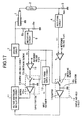
- Fig. 17 is a block diagram of a piezoelectric transformer control circuit as another modification of the third embodiment of the present invention.
- the sample-and-hold circuit 14 is inserted between the error amplifier 5 and the voltage-controlled oscillation circuit 11
- the sample-and-hold circuit 15 is inserted between the error amplifier 10 and the voltage-controlled oscillation circuit 11.
- a pulse voltage output from the pulse power supply circuit 13 operates the two sample-and-hold circuits, similar to the case of Fig. 15.
- the operations of the two sample-and-hold circuits are the same as in Fig. 15, and a description thereof will be omitted.
- the circuit in Fig. 17 can also employ the half-bridge type driving circuit 7, and the pulse oscillation circuit 16 and the AND circuit 17 instead of the pulse power supply circuit 13, similar to the case of Fig. 16.
- the piezoelectric transformer control circuit of any of the above embodiments can be preferably used not only in driving a cold-cathode fluorescent lamp as a load but also in a display device using the cold-cathode fluorescent lamp. Also, when the piezoelectric transformer control circuit is used in a computer or a personal digital assistant (PDA) including the display device, it is naturally possible to decrease the size and weight of the apparatus.
- PDA personal digital assistant
- an object when an ultraviolet lamp is driven by the piezoelectric transformer control circuit of any of the above embodiments, an object can be sterilized, deodorized, or decomposed by activation by ultraviolet rays irradiated by the lamp onto the object. That is, it is possible to provide, e.g., a sterilizing device or a water purification device using the ultraviolet lamp as a sterilization lamp or a deodorizing device using the ultraviolet lamp as a light source for exciting a catalyst.
- the piezoelectric transformer control circuit of any of the above embodiments can be used in a high-voltage generator for driving an ozone generating device or a DC-DC converter.
- a control circuit and method for a piezoelectric transformer in which a load current can be controlled to a predetermined value regardless of changes in input voltage to drive the piezoelectric transformer at a high efficiency can be provided. That is, since a load current, and a driving voltage to the piezoelectric transformer can be respectively controlled to predetermined values even if the input voltage changes, the piezoelectric transformer can be driven at a high efficiency while preventing a shift of the oscillation frequency of the piezoelectric transformer.
Landscapes
- Engineering & Computer Science (AREA)
- Power Engineering (AREA)
- Dc-Dc Converters (AREA)
- Inverter Devices (AREA)
- Details Of Television Scanning (AREA)
Claims (19)
- Steuerschaltung für einen piezoelektrischen Übertrager zum Umschalten einer Eingangs-Gleichspannung durch eine Treiberschaltung (7), um eine Wechselspannung zu erzeugen, und zum Treiben eines piezoelektrischen Übertragers (1) durch die Wechselspannung, um eine Wechsel- Hochspannung zu erhalten, umfassend:wobei das Oszillatorsignal eine Rechteckwelle ist, undeine Treiber-Detektorschaltung (8a, 8b, 9) zum Detektieren der Stärke einer Treiberspannung für den piezoelektrischen Übertrager;eine Treiberspannungs-Fehlerausgabeschaltung (10) zum Vergleichen einer Ausgangsgröße der Treiberspannungs-Detektorschaltung mit einem ersten vorbestimmten Wert, und zum Ausgeben eines Spannungsfehlerergebnisses in Form einer verstärkten Vergleichsdifferenz;eine Laststrom-Detektorschaltung (3, 4) zum Detektieren einer Stärke eines in eine an den piezoelektrischen Übertrager angeschlossene Last (2) fließenden Stroms;eine Laststrom-Fehlerausgabeschaltung (15) zum Vergleichen einer Ausgangsgröße der Laststrom-Detektorschaltung mit einem zweiten vorbestimmten Wert und zum Ausgeben eines Stromfehlerergebnisses in Form einer verstärkten Vergleichsdifferenz; undeine Oszillatorschaltung (11) zum Ausgeben eines Oszillatorsignals zum Schalten der Eingangsspannung;
wobei die Oszillatorschaltung beinhaltet:eine Frequenzeinstellschaltung (11a, 11b) zum Einstellen einer Frequenz des Oszillatorsignals nach Maßgabe des Stromfehlerergebnisses, undeine Tastverhältnis-Einstellschaltung (11b) zum Einstellen eines Tastverhältnisses des Oszillatorsignals, das von der Frequenzeinstellschaltung ausgegeeben wird, nach Maßgabe des Spannungsfehlerergebnisses. - Schaltung nach Anspruch 1, bei der die Frequenzeinstellschaltung eine Dreieckwellen-Oszillatorschaltung (11a) ist, um ansprechend auf das Stromfehlerergebnis eine Dreieckwelle auszugeben, und
die Tastverhältnis-Einstellschaltung ein Spannungsvergleicher ist zum Vergleichen der von der Dreieckwellen-Oszlllatorschaltung ausgegebenen Dreickwelle mit dem Spannungsfehlerergebnis, um das Tastverhältnis einzustellen und um die Rechteckwelle auszugeben. - Schaltung nach Anspruch 1, bei der die Frequenzeinstellschaltung eine Sägezahnwellen-Oszillatorschaltung (11c) zum Ausgeben einer Sägezahnwelle ansprechend auf das Stromfehlerergebnis ist, und
wobei die Tastverhältnis-Einstellschaltung ein Spannungsvergleicher ist zum Vergleichen der von der Sägezahnwellen-Oszillatorschaltung ausgegebenen Sägezahnwelle mit dem Spannungsfehlerergebnis, um das Tastverhältnis einzustellen und um die Rechteckwelle auszugeben. - Schaltung nach Anspruch 3, bei der die Treiberschaltung zum Treiben des piezoelektrischen Übertragers eine Halbbrücken-Treiberschaltung (7a) oder eine Vollbrücken-Treiberschaltung (7B) ist, und
die Tastverhältnis-Einstellschaltung lediglich das Hochseiten-Tastverhältnis der Brücke einstellt. - Schaltung nach Anspruch 1, weiterhin umfassend:wobei die erste Abtast- und Halteschaltung an die Treiberspannungs-Fehlerausgabeschaltung eine gehaltene Spannung ausgibt, die dem Ausgangssignal von der Treiberspannungs-Detektorschaltung während des Oszillierens entspricht, wenn die intermittierende Osziallatorschaltung nicht schwingt.eine intermittierende Oszillatorschaltung (13, 16, 17) zum Erzeugen eines Impulssignals zum intermittierenden Treiben des piezoelektrischen Übertragers und zum Zuführen des Impulssignals zu der Treiberschaltung für den piezoelektrischen Übertrager; undeine erste Abtast- und Halteschaltung (15), die zwischen der Treiberspannung-Dektektorschaltung und der Treiberspannungs-Fehlerausgabeschaltung liegt, um die Ausgangsgröße von der Treiberspannungs-Detektorschaltung nach Maßgabe des von der intermittierenden Oszillatorschaltung kommenden Impulssignals abzutasten und zu halten,
- Schaltung nach Anspruch 1, weiterhin umfassend:wobei die erste Abtast- und Halteschaltung an die Tastverhältnis-Einstellschaltung eine gehaltene Spannung ausgibt, die dem Spannungsfehlerergebnis während des Oszillierens entspricht, wenn die intermittierende Oszillatorschaltung nicht schwingt.eine intermittierende Oszillatorschaltung (13, 16, 17) zum Erzeugen eines Impulssignals zum intermittierenden Treiben des piezoelektrischen Übertragers. und zum Zuführen des Impulssignals zu der Treiberschaltung für den piezoelektrischen Übertrager; undeine erste Abtast- und Halteschaltung (15), die sich zwischen der Treiberspannungs-Fehlerausgabeschaltung und der Tastverhältnis-Einstellschaltung befindet, um das Spannungsfehlerergebnis entsprechend dem Impulssignal von der intermittierenden Oszillatorschaltung abzutasten und zu halten,
- Schaltung nach Anspruch 5, weiterhin umfassend eine zweite Abtast- und Halteschaltung (14), die sich zwischen der Laststrom-Detektorschaltung und der Laststrom-Detektor-Fehlerausgabeschaltung befindet, um das Stomfehlerergebnis abzutasten und zu erhalten,
wobei die zweite Abtast- und Halteschaltung an die Laststrom-Detektor-Fehlerausgabeschaltung eine gehaltene Spannung ausgibt, die dem Stromfehlerergebnis während des Oszillierens entspricht, wenn die intermittierende Oszillatorschaltung nicht schwingt. - Schaltung nach Anspruch 6, weiterhin umfassend eine zweite Abtast- und Halteschaltung (14), die sich zwischen der Laststrom-Detektorschaltung und der Laststrom-Detektor-Fehlerausgabeschaltung befindet, um das Stromfehlerergebnis abzutasten und zu halten,
wobei die Abtast- und Halteschaltung an die Laststrom-Detektor-Fehlerausgabeschaltung eine gehaltene Spannung ausgibt, die dem Stromfehlerergebnis während der Oszillation entspricht, wenn die intermittierende Oszillatorschaltung nicht schwingt. - Schaltung nach Anspruch 1, bei der die Steuerschaltung in einer Treibervorrichtung für eine als Last fungierende Kaltkathoden-Leuchtstofflampe verwendet wird.
- Schaltung nach Anspruch 1, bei der die Steuerschaltung in einer Treibervorrichtung für eine als Last fungierende Ultraviolettlampe verwendet wird.
- Anzeigevorrichtung, bei der eine Kaltkathoden-Leuchtstofflampe als Last von einem piezoelektrischen Übertrager gesteuert wird, der seinerseits von der Schaltung nach Anspruch 1 betrieben wird.
- Computer mit einer Anzeigevorrichtung nach Anspruch 11 als Anzeigevorrichtung.
- Persönlicher digitaler Assistent mit der Anzeigevorrichtung nach Anspruch 11 als Anzeigeeinrichtung.
- Deodorisierungsvorrichtung, mit einer Ultraviolettlampe nach Anspruch 10 als Lichtquelle für das Anregen eines Katalysators.
- Sterilisiervorrichtung mit der Ultraviolettlampe nach Anspruch 10 als Sterilisierlampe.
- Wasserreinigungsvorrichtung mit der Ultraviolettlampe nach Anspruch 10 als Sterilisierlampe.
- Schaltung nach Anspruch 1, bei der die Steuerschaltung in einem Hochspannungsgenerator für ein als Last fungierendes Ozonerzeugungsgerät verwendet wird.
- Schaltung nach Anspruch 1, bei der die Steuerschaltung in einem Gleichspannungswandler eingesetzt wird.
- Steuerverfahren für einen piezoelektrischen Übertrager zum Umschalten einer Eingangs-Gleichspannung, um eine Wechselspannung zu erzeugen, und zum Betreiben eines piezoelektrischen Übertragers (1) mit der Wechselspannung um eine Wechsel-Hochspannung zu erhalten, umfassend die Schritte:wobei das Oszillatorsignal eine Rechteckwelle ist, undeinen Treiberspannungs-Detektorschritt zum Detektieren eines Betrags einer Treiberspannung für den piezoelektrischen Übertrager;einen ersten Vergleichsschritt zum Vergleichen der detektierten Treiberspannung mit einem ersten vorbestimmten Wert und zum Verstärken eines ersten Vergleichsergebnisses;einen Laststrom-Detektorschritt zum Detektieren eines Betrags eines in einer an den piezoelektrischen Übertrager angeschlossenen Last (2) fließenden Stroms;einen zweiten Vergleichsschritt zum Vergleichen des detektierten Laststroms mit einem zweiten vorbestimmten Wert und zum Verstärken eines zweiten Vergleichsergebnisses; undeinen Oszillatorschritt zum Erzeugen eines Oszillatorsignals zum Schalten der Eingangsspannung,
wobei der Oszillatorschritt beinhaltet:einen Frequenzeinstellschritt zum Einstellen einer Frequenz des Oszillatorsignals nach Maßgabe des ersten verstärkten Vergleichsergebnisses bei dem ersten Vergleichsschritt; undeinen Tastverhältnis-Einstellschritt zum Einstellen eines Tastverhältnisses des in den Frequenzeinstellschritt eingestellten Oszillatorsignals nach Maßgabe des zweiten verstärkten Vergleichsergebnisses in dem zweiten Vergleichsschritt.
Applications Claiming Priority (7)
| Application Number | Priority Date | Filing Date | Title |
|---|---|---|---|
| JP2386897 | 1997-02-06 | ||
| JP02386997A JP3681851B2 (ja) | 1997-02-06 | 1997-02-06 | 圧電トランスの制御回路 |
| JP2386897 | 1997-02-06 | ||
| JP2386997 | 1997-02-06 | ||
| JP26042497 | 1997-09-25 | ||
| JP9260424A JPH10285942A (ja) | 1997-02-06 | 1997-09-25 | 圧電トランスの制御回路及び制御方法 |
| PCT/JP1998/000419 WO1998035434A1 (en) | 1997-02-06 | 1998-02-02 | Control circuit and method for piezoelectric transformer |
Publications (2)
| Publication Number | Publication Date |
|---|---|
| EP1016206A1 EP1016206A1 (de) | 2000-07-05 |
| EP1016206B1 true EP1016206B1 (de) | 2002-09-25 |
Family
ID=27284413
Family Applications (1)
| Application Number | Title | Priority Date | Filing Date |
|---|---|---|---|
| EP98901085A Expired - Lifetime EP1016206B1 (de) | 1997-02-06 | 1998-02-02 | Steuerschaltung und -verfahren für einen piezoelektrischen transformator |
Country Status (8)
| Country | Link |
|---|---|
| US (1) | US6198198B1 (de) |
| EP (1) | EP1016206B1 (de) |
| KR (1) | KR100360931B1 (de) |
| CN (1) | CN1118924C (de) |
| AT (1) | ATE225096T1 (de) |
| DE (1) | DE69808322T2 (de) |
| TW (1) | TW463396B (de) |
| WO (1) | WO1998035434A1 (de) |
Families Citing this family (51)
| Publication number | Priority date | Publication date | Assignee | Title |
|---|---|---|---|---|
| US6171812B1 (en) * | 1997-07-15 | 2001-01-09 | The National Institute Of Biogerontology, Inc. | Combined perfusion and mechanical loading system for explanted bone |
| EP1050954B1 (de) * | 1998-10-21 | 2004-12-15 | Matsushita Electric Industrial Co., Ltd. | Schaltung zur steuerung von piezoelektrischen transformatoren |
| JP2000268988A (ja) * | 1999-03-18 | 2000-09-29 | Nippon Soken Inc | 放電灯駆動装置 |
| US6400096B1 (en) * | 1999-08-20 | 2002-06-04 | Texas Instruments Incorporated | Control circuit for piezo transformer based fluorescent lamp power supplies |
| US6903517B2 (en) * | 2001-06-27 | 2005-06-07 | Matsushita Electric Industrial Co., Ltd. | Cold-cathode driver and liquid crystal display |
| US6853153B2 (en) * | 2002-02-26 | 2005-02-08 | Analog Microelectronics, Inc. | System and method for powering cold cathode fluorescent lighting |
| US6639367B2 (en) | 2002-02-27 | 2003-10-28 | Texas Instruments Incorporated | Control circuit employing preconditioned feedback amplifier for initializing VCO operating frequency |
| WO2003081963A1 (fr) * | 2002-03-27 | 2003-10-02 | Sanken Electric Co., Ltd. | Appareil fonctionnant avec un tube a cathode froide |
| KR20040021154A (ko) * | 2002-09-02 | 2004-03-10 | 박남식 | 오존 발생 장치 |
| JP4156324B2 (ja) | 2002-09-30 | 2008-09-24 | ローム株式会社 | 直流−交流変換装置、及び交流電力供給方法 |
| CN100429690C (zh) * | 2002-11-26 | 2008-10-29 | 华邦电子股份有限公司 | 用以控制增益错误的电流导引电路 |
| DE10259069B4 (de) * | 2002-12-17 | 2007-01-25 | Patent-Treuhand-Gesellschaft für elektrische Glühlampen mbH | Resonanzkonverter und Verfahren zum Treiben von veränderlichen Lasten |
| DE10259088B4 (de) * | 2002-12-17 | 2007-01-25 | Infineon Technologies Ag | Resonanzkonverter mit Spannungsregelung und Verfahren zum Treiben von veränderlichen Lasten |
| US7034607B2 (en) * | 2003-04-28 | 2006-04-25 | Toko Kabushiki Kaisha | Switching constant-current power device |
| EP1628388A1 (de) * | 2003-05-29 | 2006-02-22 | Tamura Corporation | Piezoelektrisches übertrageranstellverfahren und ansteuerschaltung |
| TW200527809A (en) * | 2004-01-27 | 2005-08-16 | Rohm Co Ltd | DC-AC converter, controller IC there for, and an electronic apparatus using such DC-AC converter |
| US7538473B2 (en) * | 2004-02-03 | 2009-05-26 | S.C. Johnson & Son, Inc. | Drive circuits and methods for ultrasonic piezoelectric actuators |
| US7723899B2 (en) | 2004-02-03 | 2010-05-25 | S.C. Johnson & Son, Inc. | Active material and light emitting device |
| JP2005269819A (ja) * | 2004-03-19 | 2005-09-29 | Rohm Co Ltd | 圧電トランス駆動回路及びそれを備えた冷陰極管点灯装置 |
| US7287965B2 (en) * | 2004-04-02 | 2007-10-30 | Adaptiv Energy Llc | Piezoelectric devices and methods and circuits for driving same |
| JP4561237B2 (ja) * | 2004-08-23 | 2010-10-13 | ミツミ電機株式会社 | 駆動状態検出回路 |
| CN100433528C (zh) * | 2004-11-17 | 2008-11-12 | 硕颉科技股份有限公司 | 可调变脉宽的频率控制式换流电路及其控制方法 |
| CN100463350C (zh) * | 2004-11-24 | 2009-02-18 | 新巨企业股份有限公司 | 脉动直流逆变器控制电路 |
| KR100745305B1 (ko) * | 2005-03-22 | 2007-08-01 | 주식회사 삼화양행 | 강압용 압전변압기를 사용하는 어댑터 |
| US7661229B2 (en) * | 2005-05-12 | 2010-02-16 | Worthington Armstrong Venture | Electrical conductivity in a suspended ceiling system |
| US7196475B2 (en) * | 2005-07-21 | 2007-03-27 | Canon Kabushiki Kaisha | Image forming apparatus utilizing a piezoelectric-transformer high-voltage power supply and method for controlling the same |
| KR100714633B1 (ko) * | 2006-06-20 | 2007-05-07 | 삼성전기주식회사 | Lcd 백라이트 인버터 |
| JP4062348B1 (ja) * | 2006-10-05 | 2008-03-19 | サンケン電気株式会社 | 放電管点灯装置の同期運転システム及び放電管点灯装置並びに半導体集積回路 |
| JP2008091306A (ja) * | 2006-10-05 | 2008-04-17 | Sanken Electric Co Ltd | 放電管点灯装置の周波数同期化方法及び放電管点灯装置並びに半導体集積回路 |
| US7973520B2 (en) * | 2007-08-01 | 2011-07-05 | Samsung Electronics Co., Ltd. | Piezoelectric transformer type high-voltage power apparatus and image forming apparatus |
| JP4666055B2 (ja) * | 2008-11-05 | 2011-04-06 | 日本テキサス・インスツルメンツ株式会社 | 駆動装置及び駆動方法 |
| JP5558786B2 (ja) * | 2008-12-26 | 2014-07-23 | キヤノン株式会社 | 高圧電源装置及び画像形成装置 |
| JP4902693B2 (ja) * | 2009-05-28 | 2012-03-21 | 株式会社沖データ | 圧電トランス駆動装置及び画像形成装置 |
| US8506495B2 (en) * | 2009-06-10 | 2013-08-13 | Cardiac Pacemakers, Inc. | Implantable medical devices with piezoelectric anchoring member |
| US20100317978A1 (en) * | 2009-06-10 | 2010-12-16 | Maile Keith R | Implantable medical device housing modified for piezoelectric energy harvesting |
| US8777863B2 (en) * | 2009-06-10 | 2014-07-15 | Cardiac Pacemakers, Inc. | Implantable medical device with internal piezoelectric energy harvesting |
| CN101989814B (zh) * | 2009-07-29 | 2013-10-09 | 台达电子工业股份有限公司 | 调压电路及其适用的并联式调压电路系统 |
| JP5461155B2 (ja) * | 2009-11-24 | 2014-04-02 | 澤藤電機株式会社 | パルス電圧を利用する高電圧印加装置および当該高電圧印加方法 |
| JP5731923B2 (ja) | 2010-08-04 | 2015-06-10 | 株式会社半導体エネルギー研究所 | インバータ回路、電力変換回路、及び電気推進車両 |
| WO2012029595A1 (en) * | 2010-09-03 | 2012-03-08 | Semiconductor Energy Laboratory Co., Ltd. | Oscillator circuit and semiconductor device using the oscillator circuit |
| KR101911367B1 (ko) | 2010-09-27 | 2018-10-25 | 가부시키가이샤 한도오따이 에네루기 켄큐쇼 | 기준 전류 생성 회로, 기준 전압 생성 회로, 및 온도 검출 회로 |
| JP5588891B2 (ja) * | 2011-02-21 | 2014-09-10 | ルネサスエレクトロニクス株式会社 | 圧電素子の駆動装置 |
| US20130182479A1 (en) * | 2012-01-17 | 2013-07-18 | Hamilton Sundstrand Corporation | Variable voltage reference in power rectification |
| US9650264B2 (en) | 2012-04-02 | 2017-05-16 | Calclear Investments Pty Limited | Fluid conditioning |
| US9455395B2 (en) * | 2014-01-10 | 2016-09-27 | Ecomotors, Inc. | Piezoelectric actuator control for high rate of operation |
| TWI556271B (zh) * | 2014-08-13 | 2016-11-01 | 佳世達科技股份有限公司 | 變壓器及其控制方法 |
| CN106936332B (zh) * | 2015-12-31 | 2019-11-05 | 研能科技股份有限公司 | 驱动电路及其所适用的压电致动泵 |
| TWI584574B (zh) * | 2015-12-31 | 2017-05-21 | 研能科技股份有限公司 | 驅動電路及其所適用之壓電致動泵浦 |
| TWI692192B (zh) * | 2019-05-29 | 2020-04-21 | 宏碁股份有限公司 | 可設計關機點之電源供應電路 |
| CN110342661A (zh) * | 2019-06-19 | 2019-10-18 | 北京伟思创科技股份有限公司 | 净水设备的变压器监控方法及净水设备 |
| DE102019209882A1 (de) * | 2019-07-04 | 2021-01-07 | BSH Hausgeräte GmbH | Ozonwandlervorrichtung für ein Haushaltsgerät, Haushaltsgerät sowie Verfahren |
Family Cites Families (10)
| Publication number | Priority date | Publication date | Assignee | Title |
|---|---|---|---|---|
| JPS61220386A (ja) * | 1985-03-27 | 1986-09-30 | Hitachi Ltd | 高電圧発生装置 |
| US4879528A (en) * | 1988-08-30 | 1989-11-07 | Olympus Optical Co., Ltd. | Ultrasonic oscillation circuit |
| JPH0564436A (ja) * | 1991-08-30 | 1993-03-12 | Toshiba Corp | 高圧電源装置 |
| US5424935A (en) * | 1993-06-03 | 1995-06-13 | Wu; Donald B. C. | Power converter with a piezoelectric ceramic transformer |
| DE69510835T2 (de) * | 1994-01-27 | 2000-03-16 | Hitachi Metals, Ltd. | Gerät zum Steuern einer Entladungslampe und piezoelektrischer Wandler dafür |
| JP2751842B2 (ja) * | 1994-10-05 | 1998-05-18 | 日本電気株式会社 | 圧電トランスの駆動回路および駆動方法 |
| DE69626455T2 (de) * | 1995-08-31 | 2004-01-08 | Matsushita Electric Industrial Co., Ltd., Kadoma | Umrichter mit einem piezoelektrischen Wandler |
| JP3050130B2 (ja) * | 1996-07-31 | 2000-06-12 | 日本電気株式会社 | 圧電トランスおよびその異常動作検出保護装置 |
| JP2842526B2 (ja) * | 1996-08-01 | 1999-01-06 | 日本電気株式会社 | 圧電トランスの駆動回路 |
| JP3063645B2 (ja) * | 1996-10-24 | 2000-07-12 | 日本電気株式会社 | 圧電トランスの駆動回路 |
-
1998
- 1998-02-02 EP EP98901085A patent/EP1016206B1/de not_active Expired - Lifetime
- 1998-02-02 DE DE69808322T patent/DE69808322T2/de not_active Expired - Fee Related
- 1998-02-02 WO PCT/JP1998/000419 patent/WO1998035434A1/en not_active Ceased
- 1998-02-02 AT AT98901085T patent/ATE225096T1/de not_active IP Right Cessation
- 1998-02-02 CN CN98802370A patent/CN1118924C/zh not_active Expired - Fee Related
- 1998-02-02 US US09/355,844 patent/US6198198B1/en not_active Expired - Fee Related
- 1998-02-02 KR KR1019997006962A patent/KR100360931B1/ko not_active Expired - Fee Related
- 1998-02-04 TW TW087101377A patent/TW463396B/zh not_active IP Right Cessation
Also Published As
| Publication number | Publication date |
|---|---|
| KR100360931B1 (ko) | 2002-11-18 |
| DE69808322T2 (de) | 2003-05-15 |
| DE69808322D1 (de) | 2002-10-31 |
| TW463396B (en) | 2001-11-11 |
| KR20000070712A (ko) | 2000-11-25 |
| CN1118924C (zh) | 2003-08-20 |
| EP1016206A1 (de) | 2000-07-05 |
| CN1246986A (zh) | 2000-03-08 |
| WO1998035434A1 (en) | 1998-08-13 |
| ATE225096T1 (de) | 2002-10-15 |
| US6198198B1 (en) | 2001-03-06 |
Similar Documents
| Publication | Publication Date | Title |
|---|---|---|
| US6198198B1 (en) | Control circuit and method for piezoelectric transformer | |
| US6239558B1 (en) | System for driving a cold-cathode fluorescent lamp connected to a piezoelectric transformer | |
| US6876157B2 (en) | Lamp inverter with pre-regulator | |
| US5930121A (en) | Direct drive backlight system | |
| JP2778554B2 (ja) | 圧電トランス駆動回路 | |
| US5144203A (en) | Circuit for driving an electric field luminous lamp | |
| CN100553399C (zh) | 单级背部照明反相器及其驱动方法 | |
| JP2004533800A (ja) | 電源供給装置及びこれを備えた液晶表示装置 | |
| CN1868110A (zh) | 功率变换器 | |
| JPH10285942A (ja) | 圧電トランスの制御回路及び制御方法 | |
| CN1144350C (zh) | 压电变压器逆变器 | |
| US5838113A (en) | Power supply circuit employing a differential amplifier connected to an AND gate that is in turn connected to flip-flop | |
| JP2001136749A (ja) | 圧電インバータ駆動装置 | |
| JP2817670B2 (ja) | 広入力圧電トランスインバータ | |
| US20090237346A1 (en) | Inverter circuit of driving a lamp and backlight module using the same | |
| HK1029229B (en) | Control circuit and method for piezoelectric transformer | |
| HK1029229A1 (en) | Control circuit and method for piezoelectric transformer | |
| JPH1126181A (ja) | 冷陰極管点灯装置 | |
| JP2003033046A (ja) | 圧電トランスの制御回路 | |
| JP3681851B2 (ja) | 圧電トランスの制御回路 | |
| JPH10223390A (ja) | 圧電トランスの制御回路 | |
| JPH0956175A (ja) | 圧電トランスを含む電源回路装置 | |
| JP2000166257A (ja) | 圧電トランスインバ―タ | |
| JP2000133484A (ja) | 放電管駆動回路 | |
| JP3322218B2 (ja) | 圧電トランス駆動装置及び方法 |
Legal Events
| Date | Code | Title | Description |
|---|---|---|---|
| PUAI | Public reference made under article 153(3) epc to a published international application that has entered the european phase |
Free format text: ORIGINAL CODE: 0009012 |
|
| 17P | Request for examination filed |
Effective date: 19990830 |
|
| AK | Designated contracting states |
Kind code of ref document: A1 Designated state(s): AT BE CH DE DK ES FI FR GB GR IE IT LI LU MC NL PT SE |
|
| 17Q | First examination report despatched |
Effective date: 20001227 |
|
| GRAG | Despatch of communication of intention to grant |
Free format text: ORIGINAL CODE: EPIDOS AGRA |
|
| GRAG | Despatch of communication of intention to grant |
Free format text: ORIGINAL CODE: EPIDOS AGRA |
|
| GRAG | Despatch of communication of intention to grant |
Free format text: ORIGINAL CODE: EPIDOS AGRA |
|
| GRAH | Despatch of communication of intention to grant a patent |
Free format text: ORIGINAL CODE: EPIDOS IGRA |
|
| GRAH | Despatch of communication of intention to grant a patent |
Free format text: ORIGINAL CODE: EPIDOS IGRA |
|
| GRAA | (expected) grant |
Free format text: ORIGINAL CODE: 0009210 |
|
| RAP1 | Party data changed (applicant data changed or rights of an application transferred) |
Owner name: TAIHEIYO CEMENT CORPORATION |
|
| AK | Designated contracting states |
Kind code of ref document: B1 Designated state(s): AT BE CH DE DK ES FI FR GB GR IE IT LI LU MC NL PT SE |
|
| PG25 | Lapsed in a contracting state [announced via postgrant information from national office to epo] |
Ref country code: LI Free format text: LAPSE BECAUSE OF FAILURE TO SUBMIT A TRANSLATION OF THE DESCRIPTION OR TO PAY THE FEE WITHIN THE PRESCRIBED TIME-LIMIT Effective date: 20020925 Ref country code: IT Free format text: LAPSE BECAUSE OF FAILURE TO SUBMIT A TRANSLATION OF THE DESCRIPTION OR TO PAY THE FEE WITHIN THE PRESCRIBED TIME-LIMIT;WARNING: LAPSES OF ITALIAN PATENTS WITH EFFECTIVE DATE BEFORE 2007 MAY HAVE OCCURRED AT ANY TIME BEFORE 2007. THE CORRECT EFFECTIVE DATE MAY BE DIFFERENT FROM THE ONE RECORDED. Effective date: 20020925 Ref country code: GR Free format text: LAPSE BECAUSE OF FAILURE TO SUBMIT A TRANSLATION OF THE DESCRIPTION OR TO PAY THE FEE WITHIN THE PRESCRIBED TIME-LIMIT Effective date: 20020925 Ref country code: FR Free format text: LAPSE BECAUSE OF FAILURE TO SUBMIT A TRANSLATION OF THE DESCRIPTION OR TO PAY THE FEE WITHIN THE PRESCRIBED TIME-LIMIT Effective date: 20020925 Ref country code: CH Free format text: LAPSE BECAUSE OF FAILURE TO SUBMIT A TRANSLATION OF THE DESCRIPTION OR TO PAY THE FEE WITHIN THE PRESCRIBED TIME-LIMIT Effective date: 20020925 Ref country code: BE Free format text: LAPSE BECAUSE OF FAILURE TO SUBMIT A TRANSLATION OF THE DESCRIPTION OR TO PAY THE FEE WITHIN THE PRESCRIBED TIME-LIMIT Effective date: 20020925 Ref country code: AT Free format text: LAPSE BECAUSE OF FAILURE TO SUBMIT A TRANSLATION OF THE DESCRIPTION OR TO PAY THE FEE WITHIN THE PRESCRIBED TIME-LIMIT Effective date: 20020925 |
|
| REF | Corresponds to: |
Ref document number: 225096 Country of ref document: AT Date of ref document: 20021015 Kind code of ref document: T |
|
| REG | Reference to a national code |
Ref country code: GB Ref legal event code: FG4D |
|
| REG | Reference to a national code |
Ref country code: CH Ref legal event code: EP |
|
| REG | Reference to a national code |
Ref country code: IE Ref legal event code: FG4D |
|
| REF | Corresponds to: |
Ref document number: 69808322 Country of ref document: DE Date of ref document: 20021031 |
|
| PG25 | Lapsed in a contracting state [announced via postgrant information from national office to epo] |
Ref country code: DK Free format text: LAPSE BECAUSE OF FAILURE TO SUBMIT A TRANSLATION OF THE DESCRIPTION OR TO PAY THE FEE WITHIN THE PRESCRIBED TIME-LIMIT Effective date: 20021225 |
|
| PG25 | Lapsed in a contracting state [announced via postgrant information from national office to epo] |
Ref country code: PT Free format text: LAPSE BECAUSE OF FAILURE TO SUBMIT A TRANSLATION OF THE DESCRIPTION OR TO PAY THE FEE WITHIN THE PRESCRIBED TIME-LIMIT Effective date: 20021226 |
|
| PG25 | Lapsed in a contracting state [announced via postgrant information from national office to epo] |
Ref country code: LU Free format text: LAPSE BECAUSE OF NON-PAYMENT OF DUE FEES Effective date: 20030202 |
|
| PG25 | Lapsed in a contracting state [announced via postgrant information from national office to epo] |
Ref country code: IE Free format text: LAPSE BECAUSE OF NON-PAYMENT OF DUE FEES Effective date: 20030203 |
|
| PG25 | Lapsed in a contracting state [announced via postgrant information from national office to epo] |
Ref country code: MC Free format text: LAPSE BECAUSE OF NON-PAYMENT OF DUE FEES Effective date: 20030228 |
|
| PG25 | Lapsed in a contracting state [announced via postgrant information from national office to epo] |
Ref country code: ES Free format text: LAPSE BECAUSE OF FAILURE TO SUBMIT A TRANSLATION OF THE DESCRIPTION OR TO PAY THE FEE WITHIN THE PRESCRIBED TIME-LIMIT Effective date: 20030328 |
|
| REG | Reference to a national code |
Ref country code: CH Ref legal event code: PL |
|
| EN | Fr: translation not filed | ||
| PLBE | No opposition filed within time limit |
Free format text: ORIGINAL CODE: 0009261 |
|
| STAA | Information on the status of an ep patent application or granted ep patent |
Free format text: STATUS: NO OPPOSITION FILED WITHIN TIME LIMIT |
|
| 26N | No opposition filed |
Effective date: 20030626 |
|
| REG | Reference to a national code |
Ref country code: IE Ref legal event code: MM4A |
|
| PGFP | Annual fee paid to national office [announced via postgrant information from national office to epo] |
Ref country code: SE Payment date: 20050118 Year of fee payment: 8 Ref country code: NL Payment date: 20050118 Year of fee payment: 8 Ref country code: FI Payment date: 20050118 Year of fee payment: 8 |
|
| PGFP | Annual fee paid to national office [announced via postgrant information from national office to epo] |
Ref country code: GB Payment date: 20050125 Year of fee payment: 8 |
|
| PGFP | Annual fee paid to national office [announced via postgrant information from national office to epo] |
Ref country code: DE Payment date: 20050208 Year of fee payment: 8 |
|
| PG25 | Lapsed in a contracting state [announced via postgrant information from national office to epo] |
Ref country code: GB Free format text: LAPSE BECAUSE OF NON-PAYMENT OF DUE FEES Effective date: 20060202 Ref country code: FI Free format text: LAPSE BECAUSE OF NON-PAYMENT OF DUE FEES Effective date: 20060202 |
|
| PG25 | Lapsed in a contracting state [announced via postgrant information from national office to epo] |
Ref country code: SE Free format text: LAPSE BECAUSE OF NON-PAYMENT OF DUE FEES Effective date: 20060203 |
|
| PG25 | Lapsed in a contracting state [announced via postgrant information from national office to epo] |
Ref country code: NL Free format text: LAPSE BECAUSE OF NON-PAYMENT OF DUE FEES Effective date: 20060901 Ref country code: DE Free format text: LAPSE BECAUSE OF NON-PAYMENT OF DUE FEES Effective date: 20060901 |
|
| EUG | Se: european patent has lapsed | ||
| GBPC | Gb: european patent ceased through non-payment of renewal fee |
Effective date: 20060202 |
|
| NLV4 | Nl: lapsed or anulled due to non-payment of the annual fee |
Effective date: 20060901 |