EP1016621A2 - Procédé de fabrication de pores étroits et d'une structure ayant de tels pores étroits, pores étroits et structure obtenus par ledit procédé - Google Patents
Procédé de fabrication de pores étroits et d'une structure ayant de tels pores étroits, pores étroits et structure obtenus par ledit procédé Download PDFInfo
- Publication number
- EP1016621A2 EP1016621A2 EP99310330A EP99310330A EP1016621A2 EP 1016621 A2 EP1016621 A2 EP 1016621A2 EP 99310330 A EP99310330 A EP 99310330A EP 99310330 A EP99310330 A EP 99310330A EP 1016621 A2 EP1016621 A2 EP 1016621A2
- Authority
- EP
- European Patent Office
- Prior art keywords
- workpiece
- narrow
- narrow pores
- anodic oxidation
- particle beam
- Prior art date
- Legal status (The legal status is an assumption and is not a legal conclusion. Google has not performed a legal analysis and makes no representation as to the accuracy of the status listed.)
- Granted
Links
Images





Classifications
-
- B—PERFORMING OPERATIONS; TRANSPORTING
- B82—NANOTECHNOLOGY
- B82Y—SPECIFIC USES OR APPLICATIONS OF NANOSTRUCTURES; MEASUREMENT OR ANALYSIS OF NANOSTRUCTURES; MANUFACTURE OR TREATMENT OF NANOSTRUCTURES
- B82Y15/00—Nanotechnology for interacting, sensing or actuating, e.g. quantum dots as markers in protein assays or molecular motors
-
- C—CHEMISTRY; METALLURGY
- C25—ELECTROLYTIC OR ELECTROPHORETIC PROCESSES; APPARATUS THEREFOR
- C25D—PROCESSES FOR THE ELECTROLYTIC OR ELECTROPHORETIC PRODUCTION OF COATINGS; ELECTROFORMING; APPARATUS THEREFOR
- C25D11/00—Electrolytic coating by surface reaction, i.e. forming conversion layers
- C25D11/02—Anodisation
- C25D11/022—Anodisation on selected surface areas
-
- B—PERFORMING OPERATIONS; TRANSPORTING
- B82—NANOTECHNOLOGY
- B82Y—SPECIFIC USES OR APPLICATIONS OF NANOSTRUCTURES; MEASUREMENT OR ANALYSIS OF NANOSTRUCTURES; MANUFACTURE OR TREATMENT OF NANOSTRUCTURES
- B82Y30/00—Nanotechnology for materials or surface science, e.g. nanocomposites
-
- C—CHEMISTRY; METALLURGY
- C25—ELECTROLYTIC OR ELECTROPHORETIC PROCESSES; APPARATUS THEREFOR
- C25D—PROCESSES FOR THE ELECTROLYTIC OR ELECTROPHORETIC PRODUCTION OF COATINGS; ELECTROFORMING; APPARATUS THEREFOR
- C25D11/00—Electrolytic coating by surface reaction, i.e. forming conversion layers
- C25D11/02—Anodisation
- C25D11/04—Anodisation of aluminium or alloys based thereon
- C25D11/16—Pretreatment, e.g. desmutting
-
- C—CHEMISTRY; METALLURGY
- C25—ELECTROLYTIC OR ELECTROPHORETIC PROCESSES; APPARATUS THEREFOR
- C25D—PROCESSES FOR THE ELECTROLYTIC OR ELECTROPHORETIC PRODUCTION OF COATINGS; ELECTROFORMING; APPARATUS THEREFOR
- C25D11/00—Electrolytic coating by surface reaction, i.e. forming conversion layers
- C25D11/02—Anodisation
- C25D11/04—Anodisation of aluminium or alloys based thereon
- C25D11/18—After-treatment, e.g. pore-sealing
- C25D11/20—Electrolytic after-treatment
-
- C—CHEMISTRY; METALLURGY
- C25—ELECTROLYTIC OR ELECTROPHORETIC PROCESSES; APPARATUS THEREFOR
- C25D—PROCESSES FOR THE ELECTROLYTIC OR ELECTROPHORETIC PRODUCTION OF COATINGS; ELECTROFORMING; APPARATUS THEREFOR
- C25D11/00—Electrolytic coating by surface reaction, i.e. forming conversion layers
- C25D11/02—Anodisation
- C25D11/04—Anodisation of aluminium or alloys based thereon
- C25D11/18—After-treatment, e.g. pore-sealing
- C25D11/24—Chemical after-treatment
-
- C—CHEMISTRY; METALLURGY
- C25—ELECTROLYTIC OR ELECTROPHORETIC PROCESSES; APPARATUS THEREFOR
- C25D—PROCESSES FOR THE ELECTROLYTIC OR ELECTROPHORETIC PRODUCTION OF COATINGS; ELECTROFORMING; APPARATUS THEREFOR
- C25D11/00—Electrolytic coating by surface reaction, i.e. forming conversion layers
- C25D11/02—Anodisation
- C25D11/04—Anodisation of aluminium or alloys based thereon
-
- C—CHEMISTRY; METALLURGY
- C25—ELECTROLYTIC OR ELECTROPHORETIC PROCESSES; APPARATUS THEREFOR
- C25D—PROCESSES FOR THE ELECTROLYTIC OR ELECTROPHORETIC PRODUCTION OF COATINGS; ELECTROFORMING; APPARATUS THEREFOR
- C25D11/00—Electrolytic coating by surface reaction, i.e. forming conversion layers
- C25D11/02—Anodisation
- C25D11/04—Anodisation of aluminium or alloys based thereon
- C25D11/045—Anodisation of aluminium or alloys based thereon for forming AAO templates
Definitions
- the present invention relates to a method for producing a nanostructure, and the nanostructure and, more particularly, to a method for producing a nanostructure with narrow pores, which can be utilized in a wide range of application to functional materials, structural materials, etc., for electron devices, optical devices, microdevices or the like, and the nanostructure.
- Methods for producing such nanostructures are, for example, methods for directly producing the nanostructures by semiconductor producing techniques including the fine pattern forming technologies such as the photolithography, electron beam exposure, X-ray exposure, and so on.
- An example of such self-ordering techniques is anodic oxidation which permits the nanostructure with narrow pores of the nanometer size to be produced readily and with good controllability.
- a known example is anodized alumina produced by anodizing aluminum and an alloy thereof in an acid bath.
- a porous oxide film is formed (for example, see R. C. Furneaux, W. R. Rigby & A. P. Davids, "NATURE,” Vol. 337, P147 (1989) etc.).
- a feature of this porous oxide film is the peculiar, geometrical structure in which extremely fine, cylindrical holes (nanoholes) having the diameters of several nm to several hundred nm are arranged in parallel at the spacing (cell size) of several nm to several hundred nm. These cylindrical holes have high aspect ratios and are also excellent in uniformity of sectional sizes.
- the diameter and spacing of the narrow pores can be controlled to some extent by adjusting current and/or voltage during the anodic oxidation, and the thickness of the oxide film and the depth of the narrow pores can be controlled by controlling the time of the anodic oxidation.
- the technologies are expected to be applied in many fields including quantum effect devices such as quantum wires, MIM devices, and the like, molecular sensors using the nanoholes as chemical reaction fields, and so on (Masuda "KOTAIBUTSURI” (Solid State Physics), 31, 493 (1996)).
- a method for producing a narrow pore according to the present invention comprises a step of radiating a particle beam onto a workpiece, and a step of carrying out anodic oxidation of the workpiece thus having been irradiated with the particle beam, to form a narrow pore in the workpiece.
- the particle beam is a charged particle beam, conveniently either a focussed ion beam or an electron beam.
- the step of radiating the particle beam may be a step of radiating the particle beam onto a film for restraining the anodic oxidation, which is laid on a surface of the workpiece, to selectively remove the film.
- the step of radiating the particle beam may be a step of selectively forming a film for restraining the anodic oxidation, on a surface of the workpiece from a raw material present in an atmosphere surrounding the workpiece.
- the fine-hole-formation starting points can be formed at desired positions by radiating the particle beam onto the workpiece, so that the narrow pores can be formed at the positions of the aforementioned fine-hole-formation starting points by the anodic oxidation of the workpiece. Therefore, embodiments of the present invention can permit the control of the arrangement, spacing, position, direction, etc. of the narrow pores in the structure of the nanometer scale.
- the production method of the present invention employs the radiation of a particle beam for the formation of the fine-hole-formation starting points, it can readily form the fine-hole-formation starting points with high uniformity even in a workpiece with unevenness in the surface.
- the production method of the present invention employs the radiation of a particle beam for the formation of the fine-hole-formation starting point , no pressure has to be exerted on the workpiece during the formation of the fine-hole-formation starting points. Therefore, the method of the present invention can also be applied to workpieces of low mechanical strength.
- the production method of the present invention employs a particle beam radiating apparatus with a particle beam such as a focused ion beam, electron beam or the like, the fine-hole-formation starting points can be formed by direct patterning. Therefore, the production method of the present invention does not have to include a step necessitating labor and time, such as application of resist, electron beam exposure, and removal of resist necessary for the production of stamper etc., and can form the fine-hole-formation starting points in a short time.
- the technique of anodic oxidation is preferable, because the nanostructures and narrow pores can be produced with good controllability relatively easily.
- the method of carrying out the two stages of anodic oxidation improved the verticality, linearity, and independence of narrow pores and locally formed portions with good spacing of narrow pores and good controllability of pattern, but the spacing and pattern of narrow pores were not always constant as a whole, thus posing the problem that the controllability thereof was not good.
- the method of forming the fine-hole-formation starting points by use of the stamper improved the shape and spacing of narrow pores and the controllability of pattern on one hand, but had the problems described below on the other hand.
- An object of the present invention is to solve these problems.
- an object of the present invention is to provide the technology of controlling the shape, spacing, pattern, position, direction, etc. of the narrow pores in the case of the narrow pores and the structure with narrow pores produced by the anodic oxidation.
- Another object of the present invention is to provide the technology that can produce the narrow pores and the structure with narrow pores readily and within a short time without constraints on the form of the workpiece, for example such as surface roughness, mechanical strength, existence of a film on the surface, or the like, while permitting high-precision control of the pattern position.
- a further object of the present invention is to disclose novel nanostructures and nanostructure devices on the basis of the nanostructure with narrow pores produced by applying the technology and enable the nanoholes to be used as functional materials in a variety of fields.
- a method for producing the narrow pores and the structure with narrow pores according to the present invention will be described mainly referring to Figs. 1A to 1C or Figs. 9A to 9C.
- the following steps (a) to (c) mainly correspond to Figs. 1A to 1C or Figs. 9A to 9C.
- First prepared is a workpiece 1 in which narrow pores are to be formed.
- Workpieces to which the present invention can be applied preferably include members containing the principal component of Al, but there are no specific restrictions on the materials as long as the narrow pores can be formed in the materials by the anodic oxidation.
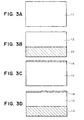
- Fig. 3A to 3D show examples of forms of workpieces to which the present invention can be applied preferably.
- the first example of the form is a bulk 11 containing Al as a principal component as illustrated in Fig. 3A.
- the bulk 11 containing the principal component of Al does not always have to be processed by mirror polishing in order to provide the surface with smoothness, and the present invention can also be applied to the bulk with the surface having some unevenness.
- the next example of the second form is a workpiece in which a film 12 containing Al as a principal component is formed on a substrate 13, as illustrated in Fig. 3B.
- the substrate 13 can be an insulating substrate of quartz glass or the like, a substrate such as a semiconductor substrate of silicon, gallium arsenic, or the like, or one in which a film of one layer or films of two or more layers are formed on these substrates.
- the materials, the thickness, the mechanical strength, etc. of the substrate 13 as long as there is no inconvenience against the formation of narrow pores by the anodic oxidation of the film 12 containing Al as a principal component.
- the uniformity can be enhanced for the depth of narrow pores.
- a method for forming the film 12 containing Al as a principal component can be any film forming method, including resistance heating evaporation, EB evaporation, sputtering, CVD, and so on.
- the present invention can also be applied to cases in which the film 12 containing Al as a principal component has surface unevenness due to existence of grains or the like.
- the next example of the third form is a workpiece in which a surface film 14 is formed on the bulk 11 containing Al as a principal component (Fig. 3C) or a workpiece in which a surface film 14 is formed on the member in which the film 12 containing Al as a principal component is formed on the substrate 13 (Fig. 3D).
- a material for the surface film 14 formed on the surface in these examples can be selected, for example, from insulators, valve metals (Nb, Ti, Ta, Zr, Hf, etc.), C, and so on, but there are no specific restrictions on the materials as long as the materials pose no inconvenience in the formation of narrow pores by the anodic oxidation.
- the surface film 14 can be not only a film of a single layer but also a film of two or more layers, and there are no specific restrictions on materials of the individual layers, a combination thereof, etc. as long as there occurs no inconvenience in the formation of narrow pores by the anodic oxidation.
- the workpiece is one in which the surface film 14 is two-layered films of an insulating film 18 and an electroconductive film 17 formed thereon as illustrated in Fig. 8A
- the resulting nanostructure will be as illustrated in Fig. 8C.
- the nanostructure thus produced can be applied to micro-electronic devices by making use of the conductive film in the top surface.
- the present invention can also be applied to workpieces in which the surface layer 14 has the surface unevenness due to the existence of grains or the like.
- the shape of the workpieces in the present invention is not limited to smooth sheets, but can be one having a curved surface or one with some unevenness or steps in the surface, or the like. There are, however, no specific restrictions on the shape as long as there is no inconvenience in the formation of narrow pores by the anodic oxidation.
- the narrow-pore-formation starting points 2 are formed at desired positions by radiating a particle beam 10 (specifically, a charged particle beam, specific examples of the charged particle beam being a focused ion beam and an electron beam) onto the above workpiece 1.
- a particle beam 10 specifically, a charged particle beam, specific examples of the charged particle beam being a focused ion beam and an electron beam
- An example of this observing means is a method of obtaining a scan image by detecting secondary electrons appearing when a sample is scanned with the particle beam such as the focused ion beam or the electron beam.
- the workpiece is exposed to the particle beam during the observation.
- influence of the exposure to the particle beam during the setting of patterning positions on the workpiece can be substantially negligible if the scan image is formed using the particle beam of sufficiently a little current.
- a method for shifting the position irradiated with the particle beam can be selected from a method for moving the irradiating position by scanning the particle beam itself or the like, a method for moving the workpiece, a method of combination of the two methods, and so on.
- the method for moving the particle beam itself is rational in terms of apparatus, but there is a limit to a movable range. Therefore, the combined method of the two methods is considered to be suitable for the formation of narrow-pore-formation starting points in a large area and in a high density.
- the present invention can also be applied with use of a sample stage permitting high-precision position control.
- Figs. 4A to 4D Figs. 9A to 9C
- Figs. 10A to 10D Figs. 11A and 11B
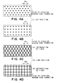
- Figs. 4A, 4C, 10A, 10C, and 11A show examples in which the narrow-pore-formation starting points are formed in an approximately honeycomb pattern.
- Figs. 4B, 4D, 10B, 10D, and 11B show examples in which the narrow-pore-formation starting points are formed in an approximately square pattern.
- a variety of examples can also be contemplated in addition to the examples described herein, and there are no specific restrictions as long as there is no inconvenience in the formation of narrow pores by the anodic oxidation.
- the forming methods of the narrow-pore-formation starting points by the irradiation with the particle beam according to the present invention can be generally classified under the following three methods.
- the first method is a method for physically and/or chemically changing the surface of the workpiece by radiating the particle beam onto the surface of the workpiece.
- the second method is a method for radiating the particle beam onto a mask (a film for restraining the anodic oxidation) formed on the surface of the workpiece to remove the mask in part to partly expose the surface of the workpiece and using the exposed portions as the narrow-pore-formation starting points.
- a mask a film for restraining the anodic oxidation
- the third method is a method for radiating the particle beam onto the surface of the workpiece to form a mask (a film for restraining the anodic oxidation) around position desired to be the narrow-pore-formation starting points on the surface of the workpiece from a raw material existing in an atmosphere surrounding the workpiece.
- the first method can be either a method of selectively radiating the particle beam onto only sites desired to be the narrow-pore-formation starting points or a method of also radiating the particle beam onto the other portions than the sites desired to be the narrow-pore-formation starting points and forming the narrow-pore-formation starting points by a difference in irradiation dose between them.
- An example of the above method of selectively radiating the particle beam onto only the sites desired to be the narrow-pore-formation starting points is a method of radiating the particle beam in a dot (circular) shape onto a plurality of areas on the workpiece (Figs. 4A and 4B), for example.
- a sequence of keeping the particle beam staying (irradiating) at a certain dot position 31 and thereafter moving the particle beam to a next dot position 31 to be kept staying thereat is carried out repeatedly. This can form the narrow-pore-formation starting points in the areas irradiated with the particle beam. If it is desired to keep the particle beam on during the movement between dots, the influence of the irradiation with the particle beam during the movement between dots can be made substantially negligible if the moving time between dots is set much shorter than the staying time at each dot position.
- An example of the method of forming the narrow-pore-formation starting points by the difference in irradiation dose with the particle beam is a method of radiating the particle beam in a line shape onto the workpiece so as to form intersections (Figs. 4C and 4D), for example.
- the particle beam is radiated in the line pattern in different directions on the workpiece to form portions (intersections) irradiated at least twice, for example.
- the workpiece is scanned in the pattern of the lines 32 in mutually different directions with the particle beam to effect irradiation only once along each line.
- the intersections 33 between the lines are irradiated plural times with the particle beam, as compared with the surroundings thereof, and thus the narrow-pore-formation starting points can be formed at the intersections 33 between the lines.
- the narrow-pore-formation starting points are formed at the positions irradiated with the particle beam or at the positions irradiated in the greater irradiation dose (the greater number of irradiation times) with the particle beam.
- the particle beam is a focused ion beam
- chemical change composition change or the like
- physical change formation of a recessed portion
- ion etching forms a state different from the surroundings in the surface of the workpiece and it serves as a specific point (a narrow-pore-formation starting point) during the anodic oxidation to advance the anodic oxidation.
- the particle beam is an electron beam
- physical change formation of a recessed portion
- the aforementioned production method is a method using the portions directly subjected to some change in the workpiece by radiating the particle beam to the surface of the workpiece, as the narrow-pore-formation starting points. It is, however, noted that the methods for forming the narrow-pore-formation starting points according to the present invention are not limited to the above method.
- the film (surface film) 14 for restraining the anodic oxidation is preliminarily laid in the surface of the workpiece, for example as illustrated in Fig. 3C, Fig. 3D, or Fig. 8A, and the particle beam is radiated onto only the desired positions of this film to remove the film in part thereby and expose the surface of the workpiece there (Fig. 8B and Figs. 11A and 11B).
- the exposed surfaces of the workpiece serve as the narrow-pore-formation starting points.
- An example of the above method of radiating the particle beam onto only the sites desired to be the narrow-pore-formation starting points is, for example, the method of radiating the particle beam in the dot (circular) shape onto the workpiece (Figs.
- the method illustrated in Figs. 11A and 11B is a method of repeatedly carrying out a process of keeping the particle beam staying at a certain dot position 31 and thereafter moving it to a next dot position 31 to keep the particle beam staying thereat. This removes the surface film 14 in the areas irradiated with the particle beam to expose the surface of the workpiece and the exposed areas can be used as the narrow-pore-formation starting points. If the particle beam is desired to be kept on during the movement between dots, the influence of the particle beam irradiation during the movement between dots can be made substantially negligible by setting the moving time between dots extremely shorter than the staying time at each dot position.
- the particle beam is radiated to desired areas on the workpiece in an atmosphere 7 containing a raw material for formation of the film for restraining the anodic oxidation, as illustrated in Fig. 9B, whereby the aforementioned film 14 for restraining the anodic oxidation can be laid at only the desired positions on the surface of the workpiece.
- the surfaces of the workpiece not irradiated with the particle beam can serve as the narrow-pore-formation starting points (Figs. 10A to 10D).
- An example of the method for forming the narrow-pore-formation starting points according to this method is, for example, a method of radiating the particle beam to the surface 35 of the workpiece except for the pattern expected to be the narrow-pore-formation starting points (the dot (circular) pattern in Figs. 10A and 10B or the rectangular pattern in Figs. 10C and 10D) to form the narrow-pore-formation starting points.
- the pattern expected to be the narrow-pore-formation starting points the dot (circular) pattern in Figs. 10A and 10B or the rectangular pattern in Figs. 10C and 10D
- the surface of the workpiece is scanned in the line pattern with the particle beam to lay lines of films for restraining the anodic oxidation at intervals, and areas 38 surrounded by the films for restraining the anodic oxidation can serve as the narrow-pore-formation starting points. Therefore, this method is preferable, because the narrow-pore-formation starting points can be formed readily.
- the films for restraining the anodic oxidation can be made, for example, of insulators, but they may also be made of conductors or semiconductors if they are materials that can restrain the anodic oxidation of workpiece. It is, however, preferable to exclude the noble metals if the conductors are used, in order to bring about the anodic oxidation stably.
- the narrow-pore-formation starting points are formed at the nonirradiated positions with the particle beam in the atmosphere containing the raw material for formation of the film for restraining the anodic oxidation.
- the above raw material is thermally decomposed or the like to form the film on the workpiece at the positions irradiated with the particle beam. It is then assumed that the film thus formed restrain the formation of narrow pore in the workpiece present immediately below the film and thus the formation (growth) of narrow pore takes place at the positions not irradiated with the particle beam.
- a first example of the type of the raw material for formation of the film for restraining the anodic oxidation is materials containing metal as a component.
- such materials include gases of metal carbonyls such as W(CO) 6 , Mo(CO) 6 and so on, organic metal compounds, metal halides, such as SiCl 4 , TiCl 4 , ZrCl 4 , TaCl 4 , MoCl 5 , WF 6 , and so on, or metal hydrides such as SiH 4 , Si 2 H 6 , and so on.
- a second example of the type of the raw material for formation of the above film for restraining the anodic oxidation is gases of organic compounds containing no metal.
- gases of organic compounds containing no metal examples include gases of aromatic compounds such as pyrene, tolunitrile, and so on, hydrocarbons such as methane, ethane, and so on, ketones such as acetone and the like, and so on. It is, however, noted that there are no specific restrictions on the types of the gases for formation of the surface film as long as there is no inconvenience in the formation of narrow pores by the anodic oxidation.
- Methods for using the raw material for the formation of the film for restraining the anodic oxidation include use of the raw material alone, use of the raw material mixed with a gas such as Ar, He, N 2 , or the like, and so on, but the methods are not limited to these methods in particular unless there is inconvenience in the formation of narrow pores by the anodic oxidation.
- the film 14 for restraining the anodic oxidation contains metal.
- W(CO) 6 is used as a raw material
- the film containing W is formed.
- the film 14 for restraining the anodic oxidation is a film containing carbon. There are, however, some cases wherein these films contain impurities of the other elements present in the atmosphere.
- the particle beam is radiated to the desired areas in the workpiece containing Al as a principal component in the atmosphere 7 containing Al(CH 3 ) 3 or AlCl 3 etc. as the above raw material, a substantially uneven Al film is formed on the surface of the workpiece. Therefore, depressed (recessed) portions of the Al film (areas not irradiated with the particle beam or areas irradiated in a smaller irradiation dose with the particle beam) can also be used as the narrow-pore-formation starting points. In this case, we can regard the Al film as the film for restraining the anodic oxidation.
- ion species thereof can be one selected from liquid metal ion sources such as Ga, Si, Ge, Cs, Nb, Cu, etc., and field ionized gas ion sources such as O, N, H, He, Ar, and so on.
- liquid metal ion sources such as Ga, Si, Ge, Cs, Nb, Cu, etc.
- field ionized gas ion sources such as O, N, H, He, Ar, and so on.
- Ga is generally used as an ion species of the focused ion beam for the reason of easiness to handle.
- the effect of ion implantation there are cases in which elements resistant to the anodic oxidation, such as the noble metals or the like, are not preferable as the ion species of the focused ion beam in the present invention. It is, however, noted that this is not the case if they are used for the formation of the film 14 for restraining the anodic oxidation described previously or for the physical deformation of the surface of the workpiece by etching or the like of the surface of workpiece.
- the effect of ion implantation varies depending upon various process conditions such as the ion species, acceleration voltage, and so on, it is desirable that the element of the ion species not less than 1 ppm be present at the narrow-pore-formation starting points.
- the energy thereof is preferably not less than 1 keV but less than 10 MeV.
- the acceleration voltage of electrons is in the range of about several kV to several MV accordingly.
- the energy of the electron beam is preferably not less than 10 keV and not more than 1 MeV for the reason of easiness to handle and the like. Therefore, the acceleration voltage of the electron beam is also preferably not less than 10 kV and not more than 1 MV.
- the narrow-pore-formation starting points can be formed at arbitrary positions. There are no specific restrictions on the spacing and pattern of the positions of the narrow-pore-formation starting points. However, with consideration to practical applications, there are cases wherein the narrow pores and the nanostructure with narrow pores are required to be formed at repetitive positions of almost identical spacing and pattern. In such cases the narrow-pore-formation starting points are formed as repetition of almost identical spacing and pattern.
- the pattern of narrow pores is apt to be repetition of a nearly honeycomb pattern because of self-organization. It is thus preferable to preliminarily form the narrow-pore-formation starting points as repetition of the nearly honeycomb pattern. This is particularly desirable in cases wherein the structure with deep narrow pores is expected to form. Since the above self-organization does not take place yet in the case of shallow narrow pores, it is also possible to form the narrow-pore-formation starting points as repetition of a pattern of an arbitrary shape such as a nearly square shape or the like, however.
- the spacing of the narrow pores in the formation of narrow pores by the anodic oxidation can be controlled to some extent by the various process conditions including the type, concentration, and temperature of an electrolytic solution used in the anodic oxidation, and a voltage applying method, a voltage value, time, etc. of the anodic oxidation. Therefore, it is preferable to preliminarily form the narrow-pore-formation starting points at the spacing of narrow pores expected from the various process conditions. For example, there is the following empirical relation between the spacing 2R (nm) of the narrow pores and the anodic oxidation voltage Va (Volt).
- the spacing (2Rv) of the narrow-pore-formation starting points according to the present invention is preferably not less than 5 nm and not more than 1000 nm in consideration of practical applications.
- An intensity distribution of the aforementioned particle beam that can be used in the present invention is an approximately Gaussian distribution. It is thus desirable that a particle-beam-irradiated area (i.e., the diameter of the particle beam) for irradiation of each narrow-pore-formation starting point not overlap with another particle-beam-irradiated area (i.e., the diameter of the particle beam) for irradiation of a next narrow-pore-formation starting point.
- the diameter of the particle beam used for radiating in the present invention is preferably not more than the spacing of the narrow-pore-formation starting points accordingly. Therefore, the diameter of the particle beam used for the working is preferably not more than 500 nm.
- the anodic oxidation operation is carried out on the workpiece 1 in which the above narrow-pore-formation starting points were formed, thereby producing the structure having the narrow pores 3 at the narrow-pore-formation starting points 2.
- Fig. 5 is a schematic diagram of an anodic oxidation apparatus used in this step.
- reference numeral 1 designates the workpiece, 41 a thermostatic water bath, 42 a cathode of a Pt sheet, 43 the electrolytic solution, 44 a reaction vessel, 45 a power supply for applying the anodic oxidation voltage, and 46 a current meter for measuring the anodic oxidation current.
- the apparatus also incorporates a computer etc. for automatic control and measurement of voltage and current in addition to the aforementioned elements, though it is omitted from the illustration.
- the workpiece 1 and cathode 42 are placed in the electrolytic solution kept at a fixed temperature by the thermostatic water bath and the anodic oxidation is started with application of the voltage between the workpiece and the cathode from the power supply.
- the electrolytic solution used in the anodic oxidation is, for example, a solution of oxalic acid, phosphoric acid, sulfuric acid, chromic acid, or the like, but there are no specific restrictions on the electrolytic solution unless there is inconvenience in the formation of narrow pores by the anodic oxidation.
- the various conditions including the anodic oxidation voltage, temperature, etc. according to each electrolytic solution can be properly set according to the nanostructure produced.
- the size of the narrow pores can be widened, if necessary, by the pore widening operation in which the above nanostructure is immersed in an acid solution (for example, a phosphoric acid solution in the case of anodized alumina).
- an acid solution for example, a phosphoric acid solution in the case of anodized alumina.
- the structure with the narrow pores in the desired size can be formed by controlling the concentration of the acid, the operation time, the temperature, and so on.
- Figs. 2A and 2B show an example (anodized alumina) of a configuration of the structure having the narrow pores according to the present invention.
- Fig. 2A is a plan view and Fig. 2B is a sectional view along a line 2B-2B of Fig. 2A.
- numeral 1 designates the workpiece, 3 the narrow pores (nanoholes), and 4 a barrier layer.
- This structure has the cylindrical narrow pores 3 and the narrow pores 3 are placed in parallel to each other and at nearly equal spacing.
- the diameter 2r of the narrow pores 3 is several nm to several hundred nm
- the spacing (cell size) 2R is about several nm to several hundred nm
- the depth is 10 nm to 100 ⁇ m.
- the spacing and the diameter of the narrow pores 3 can be controlled to some extent by the formation conditions of the narrow-pore-formation starting points and the various process conditions including the concentration and temperature of the electrolytic solution used in the anodic oxidation, the anodic oxidation voltage applying method, the voltage value, and the time, the conditions of the pore widening operation thereafter, and so on.
- the depth (length) of the narrow pores 3 can be controlled by the anodic oxidation time, the thickness of Al, and so on, and is, for example, in the range of 10 nm to 100 ⁇ m.
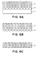
- the structure can be formed in the form wherein the narrow pores are formed up to midway as illustrated in Fig. 2B or can also be formed in the form having the narrow pores passing through the workpiece, as illustrated in Fig. 6C.
- nanostructure it is also possible to form another nanostructure, using the above structure as a mold or a mask.
- Examples of such formation of the nanostructure include formation of quantum wires by filling a functional material of a metal, a semiconductor, or the like into the narrow pores by use of the nanostructure having the narrow pores as a mold, formation of quantum dots by evaporation of a functional material of a metal, a semiconductor, or the like by use of the nanostructure having the through narrow pores as a mask for evaporation, and so on, but there are no specific restrictions on the use of the nanostructure as long as there is no inconvenience in the formation of the nanostructure.
- Fig. 7C shows an example of formation of the quantum wires by filling a filler 6 into the narrow pores 3.
- the workpiece was prepared in the form of a mirror-polished workpiece by electrolytic polishing of the surface of an A1 sheet with the purity of 99.99 % in a mixed solution of perchloric acid and ethanol.
- the focused ion beam was radiated onto the workpiece to form the narrow-pore-formation starting points (recessed portions) in the workpiece as illustrated in Fig. 1B.
- the ion species of the focused ion beam irradiation apparatus was Ga and the acceleration voltage was 30 kV.
- the positions where the narrow-pore-formation starting points were to be formed were defined using the secondary electron observing function attached to the focused ion beam irradiation apparatus. Then using the focused ion beam having the ion beam diameter of approximately 30 nm and the ion current of approximately 3 pA, the focused ion beam was radiated in the dot shape on the workpiece so as to achieve the repetition of the nearly honeycomb pattern at the spacing of about 100 nm as illustrated in Fig. 4A, thus forming the narrow-pore-formation starting points. At this time the residence time of the focused ion beam at each dot position was approximately 10 msec.
- the anodic oxidation apparatus of Fig. 5 With the anodic oxidation apparatus of Fig. 5 the anodic oxidation operation was carried out on the workpiece to form the workpiece with narrow pores as illustrated in Fig. 1C.
- the acid electrolytic solution was 0.3M oxalic acid aqueous solution, the solution was kept at 3°C by the thermostatic water bath, and the anodic oxidation voltage was approximately 40 V.
- the workpiece was then immersed in 5wt% phosphoric acid solution for 30 minutes to widen the diameter of the narrow pores.
- the workpiece was observed with FE-SEM (field emission-scanning electron microscope) and it was confirmed that the diameter of the narrow pores was approximately 50 nm and the spacing of the narrow pores was approximately 100 nm, that the narrow pores were formed as the repetition of the approximately honeycomb pattern, and that the nanostructure was formed with high regularity of the narrow pores.
- FE-SEM field emission-scanning electron microscope
- the workpiece was prepared in the form in which an Al film approximately 200 nm thick was formed on a quartz substrate by resistance heating evaporation.
- the focused ion beam irradiation apparatus With the focused ion beam irradiation apparatus the focused ion beam was radiated onto the workpiece to form the narrow-pore-formation starting points (recessed portions) in the workpiece as illustrated in Fig. 1B.
- the ion species of the focused ion beam irradiation apparatus was Ga and the acceleration voltage was 30 kV.
- the positions where the narrow-pore-formation starting points were to be formed were defined using the secondary electron observing function attached to the focused ion beam irradiation apparatus.
- the focused ion beam having the ion beam diameter of approximately 30 nm and the ion current of approximately 3 pA, the focused ion beam was radiated in the dot shape on the workpiece so as to achieve the repetition of the nearly square pattern at the spacing of about 60 nm as illustrated in Fig. 4B, thus forming the narrow-pore-formation starting points.
- the residence time of the focused ion beam at each dot position was approximately 100 msec.
- the anodic oxidation apparatus of Fig. 5 With the anodic oxidation apparatus of Fig. 5 the anodic oxidation operation was carried out on the workpiece to form the workpiece with narrow pores as illustrated in Fig. 1C.
- the acid electrolytic solution was 0.3M sulfuric acid aqueous solution, the solution was kept at 3°C by the thermostatic water bath, and the anodic oxidation voltage was approximately 25 V.
- the workpiece was then immersed in 5wt% phosphoric acid solution for 20 minutes to widen the diameter of the narrow pores.
- the workpiece was observed with FE-SEM and it was confirmed that the diameter of the narrow pores was approximately 40 nm and the spacing of the narrow pores was approximately 60 nm, that the narrow pores were formed as the repetition of the approximately square pattern, and that the nanostructure was formed with high regularity of the narrow pores.
- the workpiece was prepared in the form similar to that in Example 1.
- the focused ion beam irradiation apparatus With the focused ion beam irradiation apparatus the focused ion beam was radiated onto the workpiece to form the narrow-pore-formation starting points (recessed portions) in the workpiece as illustrated in Fig. 1B.
- the ion species of the focused ion beam irradiation apparatus was Ga and the acceleration voltage was 30 kV.
- the positions where the narrow-pore-formation starting points were to be formed were defined using the secondary electron observing function attached to the focused ion beam irradiation apparatus.
- the narrow-pore-formation starting points were formed at intersections between lines in such a manner that the focused ion beam was radiated in a line pattern to implement the repetition of nearly parallel lines at the spacing of approximately 100 nm and then the focused ion beam was radiated in a line pattern so as to implement the repetition of nearly parallel lines at the spacing of approximately 100 nm in a direction inclined at 60° to the previous lines as illustrated in Fig. 4C.
- the scan speed and the number of scan times were adjusted so that the total residence time of the focused ion beam at each intersection between lines was approximately 10 msec.
- the anodic oxidation apparatus of Fig. 5 With the anodic oxidation apparatus of Fig. 5 the anodic oxidation operation was carried out on the workpiece to form the workpiece with narrow pores as illustrated in Fig. 1C.
- the acid electrolytic solution was 0.3M oxalic acid aqueous solution, the solution was kept at 3°C by the thermostatic water bath, and the anodic oxidation voltage was approximately 50 V.
- the workpiece was then immersed in 5wt% phosphoric acid solution for 30 minutes to widen the diameter of the narrow pores.
- the workpiece was observed with FE-SEM and it was confirmed that the diameter of the narrow pores was approximately 50 nm and the spacing of the narrow pores was approximately 115 nm, that the narrow pores were formed as the repetition of the approximately honeycomb pattern, and that the nanostructure was formed with high regularity of the narrow pores.
- the workpiece 1 was prepared in such a manner that a substrate 13 was formed by depositing a Ti film, which will be used as a fine-hole terminating member 15 approximately 50 nm thick, on an Si substrate 16 by sputtering, thereafter an Al film 12 approximately 500 nm thick was deposited thereon by resistance heating evaporation, and further a surface film 14 was formed by depositing an SiO 2 film approximately 20 nm thick as an insulating film 18 by sputtering and then depositing a Pt film approximately 20 nm thick as a conductive film 17 by sputtering.
- a substrate 13 was formed by depositing a Ti film, which will be used as a fine-hole terminating member 15 approximately 50 nm thick, on an Si substrate 16 by sputtering, thereafter an Al film 12 approximately 500 nm thick was deposited thereon by resistance heating evaporation, and further a surface film 14 was formed by depositing an SiO 2 film approximately 20 nm thick as an insulating film 18 by s
- the focused ion beam irradiation apparatus With the focused ion beam irradiation apparatus the focused ion beam was radiated onto the workpiece to form the narrow-pore-formation starting points in the workpiece as illustrated in Fig. 8B.
- the ion species of the focused ion beam irradiation apparatus was Ga and the acceleration voltage was 30 kV.
- the positions where the narrow-pore-formation starting points were to be formed were defined using the secondary electron observing function attached to the focused ion beam irradiation apparatus.
- the focused ion beam having the ion beam diameter of approximately 50 nm and the ion current of approximately 60 pA, the focused ion beam was radiated in the dot shape on the workpiece so as to achieve the repetition of the nearly honeycomb pattern at the spacing of about 150 nm as illustrated in Fig. 4A, thus forming the narrow-pore-formation starting points (recessed portions).
- the residence time of the focused ion beam at each dot position was approximately 30 msec.
- the anodic oxidation apparatus of Fig. 5 With the anodic oxidation apparatus of Fig. 5 the anodic oxidation operation was carried out on the workpiece to form the workpiece with narrow pores.
- the acid electrolytic solution was 0.3M phosphoric acid aqueous solution, the solution was kept at 3°C by the thermostatic water bath, and the anodic oxidation voltage was approximately 70 V. It was confirmed here by decrease of current that the anodic oxidation proceeded up to the fine-hole terminating member during the anodic oxidation operation.
- the workpiece was then immersed in 5wt% phosphoric acid solution for 30 minutes to widen the diameter of the narrow pores (see Fig. 8C).
- the workpiece was observed with FE-SEM and it was confirmed that the diameter of the narrow pores in the surface film was approximately 50 nm, the diameter of the narrow pores in the alumina film was approximately 70 nm, and the spacing of the narrow pores was approximately 150 nm, that the narrow pores were formed as the repetition of the approximately honeycomb pattern, and that the nanostructure was formed with high regularity of the narrow pores. Electrical measurement of the workpiece was also carried out and it was confirmed that the Pt film in the surface maintained the electrically conductive property and that the electrical insulation was made between the Pt film in the surface and the Ti film as the fine-hole terminating member.
- the present example is an example in which the nanostructure with through narrow pores was produced by removing the other portions than the portion having the narrow pores.
- the anodic oxidation apparatus of Fig. 5 With the anodic oxidation apparatus of Fig. 5 the anodic oxidation operation was carried out on the workpiece to form the workpiece with narrow pores as illustrated in Fig. 1C.
- the acid electrolytic solution was 0.3M oxalic acid aqueous solution, the solution was kept at 3°C by the thermostatic water bath, and the anodic oxidation voltage was approximately 40 V.
- Figs. 6A to 6C The step of removing the other portions than the portion having the narrow pores is illustrated in Figs. 6A to 6C.
- the nanostructure as illustrated in Fig. 6A was immersed in HgCl 2 saturated solution to remove the part of Al bulk 11 of the workpiece (Fig. 6B). Then the workpiece was immersed in 5wt% phosphoric acid solution for 30 minutes to remove the barrier layer 4 and widen the diameter of the narrow pores, thereby producing the nanostructure having the through narrow pores 5 (Fig. 6C).
- the workpiece was observed with FE-SEM and it was confirmed that the diameter of the narrow pores was approximately 50 nm and the spacing of the narrow pores was approximately 100 nm, that the through narrow pores were formed as the repetition of the approximately honeycomb pattern, and that the nanostructure was formed with high regularity of the through narrow pores.
- the present example is an example in which the nanostructure (quantum wires) was produced by filling metal in the narrow pores, using the nanostructure with the narrow pores formed by the anodic oxidation, as a mold.
- the workpiece 1 was prepared in such a manner that the substrate 13 was formed by depositing a Ti film, which will be used as a fine-hole terminating member approximately 50 nm thick, on an Si substrate 16 by sputtering and thereafter an Al film 12 approximately 500 nm thick was further deposited thereon by resistance heating evaporation.
- a Ti film which will be used as a fine-hole terminating member approximately 50 nm thick
- the narrow-pore-formation starting points were formed in the workpiece by the method similar to that in (b) of Example 1 except that the residence time of the focused ion beam at each dot position was approximately 100 msec.
- Ni metal electrodeposition was carried out to fill the filler 6 in the narrow pores (Fig. 7C).
- the Ni filling was effected in such a manner that the workpiece, together with the opposed electrode of Ni, was immersed in the electrolytic solution of 0.14M NiSO 4 and 0.5M H 3 BO 3 to bring about electrodeposition to precipitate Ni in the nanoholes.
- the workpiece before the Ni filling was observed with FE-SEM and it was confirmed that the diameter of the narrow pores was approximately 50 nm and the spacing of the narrow pores was approximately 100 nm, that the narrow pores were formed as the repetition of the approximately honeycomb pattern, and that the nanostructure was formed with high regularity of the narrow pores. It was also confirmed that the narrow pores extended up to the fine-hole terminating member and that the length of the narrow pores was controlled by placing the fine-hole terminating member.
- Example 1 the nanostructure was produced by the method similar to that in Example 1 except that (b) the step of forming the narrow-pore-formation starting points in Example 1 was not carried out.
- the workpiece was prepared in the form of a mirror-polished workpiece by electrolytic polishing of the surface of the Al sheet with the purity of 99.99 % in the mixed solution of perchloric acid and ethanol.
- an electron beam was radiated onto the workpiece to form the narrow-pore-formation starting points (recessed portions) in the workpiece as illustrated in Fig. 1B.
- the acceleration voltage of the electron beam irradiation apparatus was 200 kV.
- the positions where the narrow-pore-formation starting points were to be formed were defined using the secondary electron observing function attached to the electron beam irradiation apparatus. Then using the electron beam having the beam diameter of approximately 10 nm, the electron beam was radiated in the dot shape on the workpiece so as to achieve the repetition of the nearly honeycomb pattern at the spacing (2Rv) of about 100 nm as illustrated in Fig. 4A, thus forming the narrow-pore-formation starting points.
- the anodic oxidation apparatus of Fig. 5 With the anodic oxidation apparatus of Fig. 5 the anodic oxidation operation was carried out on the workpiece to form the workpiece with narrow pores as illustrated in Fig. 1C.
- the acid electrolytic solution was 0.3M oxalic acid aqueous solution, the solution was kept at 3°C by the thermostatic water bath, and the anodic oxidation voltage was approximately 40 V.
- the workpiece was then immersed in 5wt% phosphoric acid solution for 30 minutes to widen the diameter of the narrow pores.
- the workpiece was observed with FE-SEM (field emission-scanning electron microscope) and it was confirmed that the diameter of the narrow pores was approximately 50 nm and the spacing of the narrow pores was approximately 100 nm, that the narrow pores were formed as the repetition of the approximately honeycomb pattern, and that the nanostructure was formed with high regularity of the narrow pores.
- FE-SEM field emission-scanning electron microscope
- the workpiece was prepared in the form in which the Al film 12 approximately 200 nm thick was formed on the quartz substrate 13 by resistance heating evaporation.
- the electron beam was radiated onto the workpiece to form the narrow-pore-formation starting points (recessed portions) in the workpiece as illustrated in Fig. 1B.
- the acceleration voltage of the electron beam irradiation apparatus was 200 kV.
- the positions where the narrow-pore-formation starting points (recessed portions) were to be formed were defined using the secondary electron observing function attached to the electron beam irradiation apparatus.
- the electron beam was radiated in the dot shape on the workpiece so as to achieve the repetition of the nearly square pattern at the spacing (2Rv) of about 60 nm as illustrated in Fig. 4B, thus forming the narrow-pore-formation starting points (recessed portions).
- the anodic oxidation apparatus of Fig. 5 With the anodic oxidation apparatus of Fig. 5 the anodic oxidation operation was carried out on the workpiece to form the workpiece with narrow pores as illustrated in Fig. 1C.
- the acid electrolytic solution was 0.3M sulfuric acid aqueous solution, the solution was kept at 3°C by the thermostatic water bath, and the anodic oxidation voltage was approximately 25 V.
- the workpiece was then immersed in 5wt% phosphoric acid solution for 20 minutes to widen the diameter of the narrow pores.
- the workpiece was observed with FE-SEM and it was confirmed that the diameter of the narrow pores was approximately 40 nm and the spacing of the narrow pores was approximately 60 nm, that the narrow pores were formed as the repetition of the approximately square pattern, and that the nanostructure was formed with high regularity of the narrow pores.
- the workpiece was prepared in the form similar to that in Example 7.
- the electron beam was radiated onto the workpiece to form the narrow-pore-formation starting points (recessed portions) in the workpiece as illustrated in Fig. 1B.
- the acceleration voltage of the electron beam irradiation apparatus was 200 kV.
- the positions where the narrow-pore-formation starting points (recessed portions) were to be formed were defined using the secondary electron observing function attached to the electron beam irradiation apparatus.
- the narrow-pore-formation starting points were formed at intersections between lines in such a manner that the electron beam was radiated in a line pattern to implement the repetition of nearly parallel lines at the spacing of approximately 100 nm and then the electron beam was radiated in a line pattern so as to implement the repetition of nearly parallel lines at the spacing of approximately 100 nm in a direction inclined at 60° to the previous lines as illustrated in Fig. 4C.
- the anodic oxidation apparatus of Fig. 5 With the anodic oxidation apparatus of Fig. 5 the anodic oxidation operation was carried out on the workpiece to form the workpiece with narrow pores as illustrated in Fig. 1C.
- the acid electrolytic solution was 0.3M oxalic acid aqueous solution, the solution was kept at 3°C by the thermostatic water bath, and the anodic oxidation voltage was approximately 50 V.
- the workpiece was then immersed in 5wt% phosphoric acid solution for 30 minutes to widen the diameter of the narrow pores.
- the workpiece was observed with FE-SEM and it was confirmed that the diameter of the narrow pores was approximately 50 nm and the spacing of the narrow pores was approximately 115 nm, that the narrow pores were formed as the repetition of the approximately honeycomb pattern, and that the nanostructure was formed with high regularity of the narrow pores.
- the workpiece 1 was prepared in such a manner that the substrate 13 was formed by depositing the Ti film, which will be used as a fine-hole terminating member 15 approximately 50 nm thick, on the Si substrate 16 by sputtering, thereafter the Al film 12 approximately 500 nm thick was deposited by resistance heating evaporation, and further the surface film 14 was formed by depositing an SiO 2 film approximately 20 nm thick as the insulating film 18 by sputtering and then depositing a Pt film approximately 20 nm thick as the conductive film 17 by sputtering.
- the electron beam was radiated onto the workpiece to form the narrow-pore-formation starting points (recessed portions) 2 in the workpiece as illustrated in Fig. 8B.
- the acceleration voltage of the electron beam irradiation apparatus was 200 kV.
- the positions where the narrow-pore-formation starting points (recessed portions) were to be formed were defined using the secondary electron observing function attached to the electron beam irradiation apparatus.
- the electron beam was radiated in the dot shape on the workpiece so as to achieve the repetition of the nearly honeycomb pattern at the spacing of about 150 nm as illustrated in Fig. 4A, thus forming the narrow-pore-formation starting points (recessed portions).
- the anodic oxidation apparatus of Fig. 5 With the anodic oxidation apparatus of Fig. 5 the anodic oxidation operation was carried out on the workpiece to form the workpiece with narrow pores.
- the acid electrolytic solution was 0.3M phosphoric acid aqueous solution, the solution was kept at 3°C by the thermostatic water bath, and the anodic oxidation voltage was approximately 70 V. It was confirmed here by decrease of current that the anodic oxidation proceeded up to the fine-hole terminating member during the anodic oxidation operation.
- the workpiece was then immersed in 5wt% phosphoric acid solution for 30 minutes to widen the diameter of the narrow pores (see Fig. 8C).
- the workpiece was observed with FE-SEM and it was confirmed that the diameter of the narrow pores in the surface film was approximately 50 nm, the diameter of the narrow pores in the alumina film was approximately 70 nm, and the spacing of the narrow pores was approximately 150 nm, that the narrow pores were formed as the repetition of the approximately honeycomb pattern, and that the nanostructure was formed with high regularity of the narrow pores. Electrical measurement of the workpiece was also carried out and it was confirmed that the Pt film in the surface maintained the electrically conductive property and that the electrical insulation was made between the Pt film in the surface and the Ti film as the fine-hole terminating member.
- the present example is an example in which the structure having the through narrow pores was produced.
- (a) Preparation of workpiece and (b) step of forming narrow-pore-formation starting points (recessed portions) were carried out using the methods similar to those in (a) and (b) of Example 7.
- the anodic oxidation apparatus of Fig. 5 With the anodic oxidation apparatus of Fig. 5 the anodic oxidation operation was carried out on the workpiece to form the workpiece with narrow pores as illustrated in Fig. 1C.
- the acid electrolytic solution was 0.3M oxalic acid aqueous solution, the solution was kept at 3°C by the thermostatic water bath, and the anodic oxidation voltage was approximately 40 V.
- Figs. 6A to 6C The step of removing the other portions than the portion having the narrow pores is illustrated in Figs. 6A to 6C.
- the nanostructure as illustrated in Fig. 6A was immersed in HgCl 2 saturated solution to remove the part of Al bulk 11 of the workpiece (Fig. 6B). Then the workpiece was immersed in 5wt% phosphoric acid solution for 30 minutes to remove the barrier layer 4 and widen the diameter of the narrow pores, thereby producing the nanostructure having the through narrow pores 5 (Fig. 6C).
- the workpiece was observed with FE-SEM and it was confirmed that the diameter of the narrow pores was approximately 50 nm and the spacing of the narrow pores was approximately 100 nm, that the through narrow pores were formed as the repetition of the approximately honeycomb pattern, and the nanostructure was formed with high regularity of the through narrow pores.
- the present example is an example in which the nanostructure (quantum wires) was produced by filling the metal in the narrow pores, using the nanostructure formed by the anodic oxidation, as a mold.
- the workpiece 1 was prepared in such a manner that the substrate 13 was formed by depositing a Ti film, which will be used as a fine-hole terminating member approximately 50 nm thick, on the Si substrate 16 by sputtering and thereafter the A1 film 12 approximately 500 nm thick was further deposited thereon by resistance heating evaporation.
- a Ti film which will be used as a fine-hole terminating member approximately 50 nm thick
- Ni metal electrodeposition was carried out to fill the filler 6 in the narrow pores (Fig. 7C).
- the Ni filling was effected in such a manner that the workpiece, together with the opposed electrode of Ni, was immersed in the electrolytic solution of 0.14M NiSO 4 and 0.5M H 3 BO 3 to bring about electrodeposition to precipitate Ni in the nanoholes.
- the workpiece before the Ni filling was observed with FE-SEM and it was confirmed that the diameter of the narrow pores was approximately 50 nm and the spacing of the narrow pores was approximately 100 nm, that the narrow pores were formed as the repetition of the approximately honeycomb pattern, and that the nanostructure was formed with high regularity of the narrow pores. It was also confirmed that the narrow pores extended up to the fine-hole terminating member and that the length of the narrow pores was controlled by placing the fine-hole terminating member.
- the workpiece after the Ni filling was observed with FE-SEM and it was confirmed that the narrow pores were filled with Ni and the quantum wires of Ni were formed in the thickness of about 50 nm.
- the workpiece was prepared in the form of a mirror-polished workpiece by electrolytic polishing of the surface of the A1 sheet with the purity of 99.99 % in the mixed solution of perchloric acid and ethanol.
- the focused ion beam was radiated onto the workpiece to form the narrow-pore-formation starting points 2 on the workpiece as illustrated in Fig. 9B.
- the ion species of the focused ion beam irradiation apparatus was Ga and the acceleration voltage was 30 kV.
- the positions where the narrow-pore-formation starting points (recessed portions) were to be formed were defined using the secondary electron observing function attached to the focused ion beam irradiation apparatus. Then pyrene gas as a gas for formation of the surface layer was introduced into the focused ion beam irradiation apparatus. Further, using the focused ion beam having the ion beam diameter of about 30 nm and the ion current of about 3 pA, the narrow-pore-formation starting points (recessed portions) were formed by radiating the focused ion beam so that the positions not irradiated with the focused ion beam were the repetition of the approximately honeycomb pattern at the spacing of about 150 nm as illustrated in Fig. 10A. At this time the surface film containing C was formed at the positions irradiated with the focused ion beam.
- the anodic oxidation apparatus of Fig. 5 With the anodic oxidation apparatus of Fig. 5 the anodic oxidation operation was carried out on the workpiece to form the workpiece with narrow pores as illustrated in Fig. 9C.
- the acid electrolytic solution was 0.3M phosphoric acid aqueous solution, the solution was kept at 3°C by the thermostatic water bath, and the anodic oxidation voltage was approximately 70 V.
- the workpiece was then immersed in 5wt% phosphoric acid solution for 30 minutes to widen the diameter of the narrow pores.
- the workpiece was observed with FE-SEM (field emission scanning electron microscope) and it was confirmed that the diameter of the narrow pores was approximately 50 nm and the spacing of the narrow pores was approximately 150 nm, that the narrow pores were formed as the repetition of the approximately honeycomb pattern, and that the nanostructure was formed with high regularity of the narrow pores.
- the workpiece was prepared in the form in which the Al film 12 approximately 200 nm thick was formed on the quartz substrate 13 by resistance heating evaporation.
- the focused ion beam was radiated onto the workpiece to form the narrow-pore-formation starting points 2 on the workpiece as illustrated in Fig. 9B.
- the ion species of the focused ion beam irradiation apparatus was Ga and the acceleration voltage was 30 kV.
- the positions where the narrow-pore-formation starting points (recessed portions) were to be formed were defined using the secondary electron observing function attached to the focused ion beam irradiation apparatus. Then the pyrene gas as a gas for formation of the surface layer was introduced into the focused ion beam irradiation apparatus. Further, using the focused ion beam having the ion beam diameter of about 30 nm and the ion current of about 3 pA, the narrow-pore-formation starting points (recessed portions) were formed by radiating the focused ion beam so that the positions not irradiated with the focused ion beam were the repetition of the approximately square pattern at the spacing of about 150 nm as illustrated in Fig. 10B. At this time the surface film containing C was formed at the positions irradiated with the focused ion beam.
- the anodic oxidation apparatus of Fig. 5 With the anodic oxidation apparatus of Fig. 5 the anodic oxidation operation was carried out on the workpiece to form the workpiece with narrow pores as illustrated in Fig. 9C.
- the acid electrolytic solution was 0.3M oxalic acid aqueous solution, the solution was kept at 3°C by the thermostatic water bath, and the anodic oxidation voltage was approximately 60 V.
- the workpiece was then immersed in 5wt% phosphoric acid solution for 30 minutes to widen the diameter of the narrow pores.
- the workpiece was observed with FE-SEM and it was confirmed that the diameter of the narrow pores was approximately 50 nm and the spacing of the narrow pores was approximately 150 nm, that the narrow pores were formed as the repetition of the approximately square pattern, and that the nanostructure was formed with high regularity of the narrow pores.
- the workpiece was prepared in the form similar to that in Example 13.
- the focused ion beam was radiated onto the workpiece to form the narrow-pore-formation starting points 2 on the workpiece as illustrated in Fig. 9B.
- the ion species of the focused ion beam irradiation apparatus was Ga and the acceleration voltage was 30 kV.
- the positions where the narrow-pore-formation starting points (recessed portions) were to be formed were defined using the secondary electron observing function attached to the focused ion beam irradiation apparatus. Then W(CO) 6 gas as a gas for formation of the surface film was introduced into the focused ion beam irradiation apparatus.
- the narrow-pore-formation starting points were formed in the areas surrounded by lines in such a manner that the focused ion beam was radiated in a line pattern to implement the repetition of nearly parallel lines at the spacing of approximately 150 nm and then the focused ion beam was radiated in a line pattern so as to implement the repetition of nearly parallel lines at the spacing of approximately 150 nm in a direction inclined at 60° to the previous lines as illustrated in Fig. 10C.
- the surface film containing W was formed at the positions irradiated with the focused ion beam.
- the anodic oxidation apparatus of Fig. 5 With the anodic oxidation apparatus of Fig. 5 the anodic oxidation operation was carried out on the workpiece to form the workpiece with narrow pores as illustrated in Fig. 9C.
- the acid electrolytic solution was 0.3M phosphoric acid aqueous solution, the solution was kept at 3°C by the thermostatic water bath, and the anodic oxidation voltage was approximately 80 V.
- the workpiece was then immersed in 5wt% phosphoric acid solution for 30 minutes to widen the diameter of the narrow pores.
- the workpiece was observed with FE-SEM and it was confirmed that the diameter of the narrow pores was approximately 50 nm and the spacing of the narrow pores was approximately 170 nm, that the narrow pores were formed as the repetition of the approximately honeycomb pattern, and that the nanostructure was formed with high regularity of the narrow pores.
- the present example is an example in which the nanostructure with through narrow pores was produced by removing the other portions than the portion having the narrow pores.
- the anodic oxidation apparatus of Fig. 5 With the anodic oxidation apparatus of Fig. 5 the anodic oxidation operation was carried out on the workpiece to form the workpiece with narrow pores as illustrated in Fig. 9C.
- the acid electrolytic solution was 0.3M oxalic acid aqueous solution, the solution was kept at 3°C by the thermostatic water bath, and the anodic oxidation voltage was approximately 70 V.
- Figs. 6A to 6C The step of removing the other portions than the portion having the narrow pores is illustrated in Figs. 6A to 6C.
- the surface layer 14 was removed by Ar ion etching of the workpiece as illustrated in Fig. 9C (Fig. 6A). Then the workpiece was immersed in HgCl 2 saturated solution to remove the part of Al bulk 11 of the workpiece (Fig. 6B). Then the workpiece was immersed in 5wt% phosphoric acid solution for 30 minutes to remove the barrier layer 4 and widen the diameter of the narrow pores, thereby producing the nanostructure having the through narrow pores 5 (Fig. 6C).
- the workpiece was observed with FE-SEM and it was confirmed that the diameter of the narrow pores was approximately 50 nm and the spacing of the narrow pores was approximately 150 nm, that the through narrow pores were formed as the repetition of the approximately honeycomb pattern, and that the nanostructure was formed with high regularity of the through narrow pores.
- the present example is an example in which the nanostructure (quantum wires) was produced by filling the metal in the narrow pores, using the nanostructure with the narrow pores formed by the anodic oxidation, as a mold.
- the workpiece 1 was prepared in such a manner that the substrate 13 was formed by depositing the Ti film, which will be used as a fine-hole terminating member approximately 50 nm thick, on the Si substrate 16 by sputtering and thereafter the Al film 12 approximately 500 nm thick was further deposited thereon by resistance heating evaporation.
- Ni metal electrodeposition was carried out to fill the filler 6 in the narrow pores (Fig. 7C).
- the Ni filling was effected in such a manner that the workpiece, together with the opposed electrode of Ni, was immersed in the electrolytic solution of 0.14M NiSO 4 and 0.5M H 3 BO 3 to bring about electrodeposition to precipitate Ni in the nanoholes.
- the workpiece before the Ni filling was observed with FE-SEM and it was confirmed that the diameter of the narrow pores was approximately 50 nm and the spacing of the narrow pores was approximately 150 nm, that the narrow pores were formed as the repetition of the approximately honeycomb pattern, and that the nanostructure was formed with high regularity of the narrow pores. It was also confirmed that the narrow pores extended up to the fine-hole terminating member and the length of the narrow pores was controlled by placing the fine-hole terminating member.
- the workpiece was prepared in the form of a mirror-polished workpiece by electrolytic polishing of the surface of the A1 sheet with the purity of 99.99 % in the mixed solution of perchloric acid and ethanol.
- the electron beam was radiated onto the workpiece to form the narrow-pore-formation starting points 2 on the workpiece as illustrated in Fig. 9B.
- the acceleration voltage of the electron beam irradiation apparatus was 200 kV.
- the positions where the narrow-pore-formation starting points 2 were to be formed were defined using the secondary electron observing function attached to the electron beam irradiation apparatus. Then the pyrene gas as a gas for formation of the surface film was introduced into the electron beam irradiation apparatus. Further, using the electron beam having the beam diameter of about 10 nm, the narrow-pore-formation starting points (recessed portions) were formed by radiating the electron beam so that the positions not irradiated with the electron beam were the repetition of the approximately honeycomb pattern at the spacing of about 150 nm as illustrated in Fig. 10A. At this time the surface film containing C was formed at the positions irradiated with the electron beam.
- the anodic oxidation apparatus of Fig. 5 With the anodic oxidation apparatus of Fig. 5 the anodic oxidation operation was carried out on the workpiece to form the workpiece with narrow pores as illustrated in Fig. 9C.
- the acid electrolytic solution was 0.3M phosphoric acid aqueous solution, the solution was kept at 3°C by the thermostatic water bath, and the anodic oxidation voltage was approximately 70 V.
- the workpiece was then immersed in 5wt% phosphoric acid solution for 30 minutes to widen the diameter of the narrow pores.
- the workpiece was observed with FE-SEM (field emission scanning electron microscope) and it was confirmed that the diameter of the narrow pores was approximately 50 nm and the spacing of the narrow pores was approximately 150 nm, that the narrow pores were formed as the repetition of the approximately honeycomb pattern, and that the nanostructure was formed with high regularity of the narrow pores.
- the workpiece was prepared in the form in which the Al film approximately 200 nm thick was formed on the quartz substrate by resistance heating evaporation.
- the electron beam was radiated onto the workpiece to form the narrow-pore-formation starting points 2 on the workpiece as illustrated in Fig. 9B.
- the acceleration voltage of the electron beam irradiation apparatus was 200 kV.
- the positions where the narrow-pore-formation starting points (recessed portions) were to be formed were defined using the secondary electron observing function attached to the electron beam irradiation apparatus. Then the pyrene gas as a gas for formation of the surface film was introduced into the electron beam irradiation apparatus. Further, using the electron beam having the beam diameter of about 10 nm, the narrow-pore-formation starting points (recessed portions) were formed by radiating the electron beam so that the positions not irradiated with the electron beam were the repetition of the approximately square pattern at the spacing of about 150 nm as illustrated in Fig. 10B. At this time the surface film containing C was formed at the positions irradiated with the electron beam.
- the anodic oxidation apparatus of Fig. 5 With the anodic oxidation apparatus of Fig. 5 the anodic oxidation operation was carried out on the workpiece to form the workpiece with narrow pores as illustrated in Fig. 9C.
- the acid electrolytic solution was 0.3M oxalic acid aqueous solution, the solution was kept at 3°C by the thermostatic water bath, and the anodic oxidation voltage was approximately 60 V.
- the workpiece was then immersed in 5wt% phosphoric acid solution for 30 minutes to widen the diameter of the narrow pores.
- the workpiece was observed with FE-SEM and it was confirmed that the diameter of the narrow pores was approximately 50 nm and the spacing of the narrow pores was approximately 150 nm, that the narrow pores were formed as the repetition of the approximately square pattern, and that the nanostructure was formed with high regularity of the narrow pores.
- the workpiece was prepared in the form similar to that in Example 18.
- the electron beam was radiated onto the workpiece to form the narrow-pore-formation starting points 2 on the workpiece as illustrated in Fig. 9B.
- the acceleration voltage of the electron beam irradiation apparatus was 200 kV.
- the positions where the narrow-pore-formation starting points (recessed portions) were to be formed were defined using the secondary electron observing function attached to the electron beam irradiation apparatus. Then the W(CO) 6 gas as a gas for formation of the surface film was introduced into the electron beam irradiation apparatus.
- the narrow-pore-formation starting points were formed in the areas surrounded by lines in such a manner that the electron beam was radiated in a line pattern to implement the repetition of nearly parallel lines at the spacing of approximately 150 nm and then the electron beam was radiated in a line pattern so as to implement the repetition of nearly parallel lines at the spacing of approximately 150 nm in a direction inclined at 60° to the previous lines as illustrated in Fig. 10C.
- the surface film containing W was formed at the positions irradiated with the electron beam.
- the anodic oxidation apparatus of Fig. 5 With the anodic oxidation apparatus of Fig. 5 the anodic oxidation operation was carried out on the workpiece to form the workpiece with narrow pores as illustrated in Fig. 9C.
- the acid electrolytic solution was 0.3M phosphoric acid aqueous solution, the solution was kept at 3°C by the thermostatic water bath, and the anodic oxidation voltage was approximately 80 V.
- the workpiece was then immersed in 5wt% phosphoric acid solution for 30 minutes to widen the diameter of the narrow pores.
- the workpiece was observed with FE-SEM and it was confirmed that the diameter of the narrow pores was approximately 50 nm and the spacing of the narrow pores was approximately 170 nm, that the narrow pores were formed as the repetition of the approximately honeycomb pattern, and that the nanostructure was formed with high regularity of the narrow pores.
- the present example is an example in which the nanostructure with through narrow pores was produced by removing the other portions than the portion having the narrow pores.
- the anodic oxidation apparatus of Fig. 5 With the anodic oxidation apparatus of Fig. 5 the anodic oxidation operation was carried out on the workpiece to form the workpiece with narrow pores as illustrated in Fig. 9C.
- the acid electrolytic solution was 0.3M oxalic acid aqueous solution, the solution was kept at 3°C by the thermostatic water bath, and the anodic oxidation voltage was approximately 70 V.
- Figs. 6A to 6C The step of removing the other portions than the portion having the narrow pores is illustrated in Figs. 6A to 6C.
- the surface film 14 was removed by Ar ion etching of the workpiece as illustrated in Fig. 9C (Fig. 6A). Then the surface film was immersed in the HgCl 2 saturated solution to remove the part of Al bulk 11 of the workpiece (Fig. 6B). Then the workpiece was immersed in 5wt% phosphoric acid solution for 30 minutes to remove the barrier layer 4 and widen the diameter of the narrow pores, thereby producing the nanostructure having the through narrow pores 5 (Fig. 6C).
- the workpiece was observed with FE-SEM and it was confirmed that the diameter of the narrow pores was approximately 50 nm and the spacing of the narrow pores was approximately 150 nm, that the through narrow pores were formed as the repetition of the approximately honeycomb pattern, and that the nanostructure was formed with high regularity of the through narrow pores.
- the present example is an example in which the nanostructure (quantum wires) was produced by filling the metal in the narrow pores, using the nanostructure with the narrow pores formed by the anodic oxidation, as a mold.
- the workpiece 1 was prepared in such a manner that the substrate 13 was formed by depositing the Ti film, which will be used as a fine-hole terminating member approximately 50 nm thick, on the Si substrate 16 by sputtering and thereafter the Al film 12 approximately 500 nm thick was further deposited thereon by resistance heating evaporation.
- the narrow-pore-formation starting points (recessed portions) were formed in the workpiece by the method similar to that in (b) of Example 18.
- Ni metal electrodeposition was carried out to fill the filler 6 in the narrow pores (Fig. 7C).
- the Ni filling was effected in such a manner that the workpiece, together with the opposed electrode of Ni, was immersed in the electrolytic solution of 0.14M NiSO 4 and 0.5M HBO 3 to bring about electrodeposition to precipitate Ni in the nanoholes.
- the workpiece before the Ni filling was observed with FE-SEM and it was confirmed that the diameter of the narrow pores was approximately 50 nm and the spacing of the narrow pores was approximately 150 nm, that the narrow pores were formed as the repetition of the approximately honeycomb pattern, and that the nanostructure was formed with high regularity of the narrow pores. It was also confirmed that the narrow pores extended up to the fine-hole terminating member and the length of the narrow pores was controlled by placing the fine-hole terminating member.
- the workpiece after the Ni filling was observed with FE-SEM and it was confirmed that the narrow pores were filled with Ni and the quantum wires of Ni were formed in the thickness of about 50 nm.
- the present invention presents the following effects.
Landscapes
- Chemical & Material Sciences (AREA)
- Engineering & Computer Science (AREA)
- Materials Engineering (AREA)
- Chemical Kinetics & Catalysis (AREA)
- Electrochemistry (AREA)
- Metallurgy (AREA)
- Organic Chemistry (AREA)
- Nanotechnology (AREA)
- Crystallography & Structural Chemistry (AREA)
- General Health & Medical Sciences (AREA)
- Life Sciences & Earth Sciences (AREA)
- Molecular Biology (AREA)
- Health & Medical Sciences (AREA)
- General Chemical & Material Sciences (AREA)
- Physics & Mathematics (AREA)
- Composite Materials (AREA)
- Condensed Matter Physics & Semiconductors (AREA)
- General Physics & Mathematics (AREA)
- Micromachines (AREA)
- Welding Or Cutting Using Electron Beams (AREA)
- Physical Or Chemical Processes And Apparatus (AREA)
- Cold Cathode And The Manufacture (AREA)
Applications Claiming Priority (10)
| Application Number | Priority Date | Filing Date | Title |
|---|---|---|---|
| JP36873798 | 1998-12-25 | ||
| JP36873798 | 1998-12-25 | ||
| JP4753999 | 1999-02-25 | ||
| JP4753999 | 1999-02-25 | ||
| JP21688699 | 1999-07-30 | ||
| JP21687099 | 1999-07-30 | ||
| JP21688699 | 1999-07-30 | ||
| JP21687099 | 1999-07-30 | ||
| JP34413499 | 1999-12-03 | ||
| JP34413499A JP4532634B2 (ja) | 1998-12-25 | 1999-12-03 | 細孔の製造方法 |
Publications (3)
| Publication Number | Publication Date |
|---|---|
| EP1016621A2 true EP1016621A2 (fr) | 2000-07-05 |
| EP1016621A3 EP1016621A3 (fr) | 2001-11-07 |
| EP1016621B1 EP1016621B1 (fr) | 2008-12-31 |
Family
ID=27522635
Family Applications (1)
| Application Number | Title | Priority Date | Filing Date |
|---|---|---|---|
| EP99310330A Expired - Lifetime EP1016621B1 (fr) | 1998-12-25 | 1999-12-21 | Procédé de fabrication de pores étroits et d'une structure ayant de tels pores étroits, pores étroits et structure obtenus par ledit procédé |
Country Status (4)
| Country | Link |
|---|---|
| US (2) | US6214738B1 (fr) |
| EP (1) | EP1016621B1 (fr) |
| JP (1) | JP4532634B2 (fr) |
| DE (1) | DE69940190D1 (fr) |
Cited By (10)
| Publication number | Priority date | Publication date | Assignee | Title |
|---|---|---|---|---|
| DE10064520A1 (de) * | 2000-12-22 | 2002-07-04 | Daimler Chrysler Ag | Verfahren zur Herstellung von selbstreinigenden Oberflächenstrukturen |
| WO2003004253A1 (fr) * | 2001-07-02 | 2003-01-16 | Alcove Surfaces Gmbh | Moule de coulee et utilisation d'une couche superficielle ayant subie une oxydation anodique |
| DE10138981A1 (de) * | 2001-08-08 | 2003-03-06 | Infineon Technologies Ag | Verfahren zur elektrochemischen Oxidation eines Halbleiter-Substrats |
| US7066234B2 (en) | 2001-04-25 | 2006-06-27 | Alcove Surfaces Gmbh | Stamping tool, casting mold and methods for structuring a surface of a work piece |
| WO2007044108A1 (fr) * | 2005-10-13 | 2007-04-19 | Hewlett-Packard Development Company, L.P. | Guide d'ondes comportant un substrat à faible indice de réfraction |
| EP1580305A3 (fr) * | 2004-03-23 | 2008-01-16 | FUJIFILM Corporation | Surface structurelle d'un corps et méthode pour sa production |
| EP2000793A3 (fr) * | 2007-06-08 | 2010-03-24 | FUJIFILM Corporation | Microstructures, procédé de production de microstructures et dispositif d'amplification du champ optique |
| CN103038870A (zh) * | 2010-07-02 | 2013-04-10 | 新南创新私人有限公司 | 用于太阳能电池的金属触点方案 |
| EP2299452A4 (fr) * | 2008-07-09 | 2017-08-02 | FUJIFILM Corporation | Microstructure et son procede de fabrication |
| EP1976007B1 (fr) * | 2007-03-27 | 2017-11-29 | Fujifilm Corporation | Procédé de fabrication d'élément conducteur anisotrope |
Families Citing this family (52)
| Publication number | Priority date | Publication date | Assignee | Title |
|---|---|---|---|---|
| JP4146978B2 (ja) * | 1999-01-06 | 2008-09-10 | キヤノン株式会社 | 細孔を有する構造体の製造方法、該製造方法により製造された構造体 |
| JP3387897B2 (ja) * | 1999-08-30 | 2003-03-17 | キヤノン株式会社 | 構造体の製造方法、並びに該製造方法により製造される構造体及び該構造体を用いた構造体デバイス |
| JP3754876B2 (ja) | 2000-07-03 | 2006-03-15 | キヤノン株式会社 | 細孔を有する構造体の製造方法及び細孔を有する構造体 |
| US7041394B2 (en) * | 2001-03-15 | 2006-05-09 | Seagate Technology Llc | Magnetic recording media having self organized magnetic arrays |
| US7153597B2 (en) * | 2001-03-15 | 2006-12-26 | Seagate Technology Llc | Magnetic recording media having chemically modified patterned substrate to assemble self organized magnetic arrays |
| JP2002356400A (ja) * | 2001-03-22 | 2002-12-13 | Canon Inc | 酸化亜鉛の針状構造体の製造方法及びそれを用いた電池、光電変換装置 |
| US20020145826A1 (en) * | 2001-04-09 | 2002-10-10 | University Of Alabama | Method for the preparation of nanometer scale particle arrays and the particle arrays prepared thereby |
| US6804081B2 (en) * | 2001-05-11 | 2004-10-12 | Canon Kabushiki Kaisha | Structure having pores and its manufacturing method |
| US7079250B2 (en) * | 2002-01-08 | 2006-07-18 | Fuji Photo Film Co., Ltd. | Structure, structure manufacturing method and sensor using the same |
| ITTO20020033A1 (it) * | 2002-01-11 | 2003-07-11 | Fiat Ricerche | Dispositivo elettro-luminescente. |
| AU2003213353A1 (en) * | 2002-03-15 | 2003-09-29 | Canon Kabushiki Kaisha | Porous material and process for producing the same |
| AU2003221365A1 (en) * | 2002-03-15 | 2003-09-29 | Canon Kabushiki Kaisha | Porous material and process for producing the same |
| US6878634B2 (en) * | 2002-04-10 | 2005-04-12 | Canon Kabushiki Kaisha | Structure having recesses and projections, method of manufacturing structure, and functional device |
| JP3848303B2 (ja) * | 2002-06-07 | 2006-11-22 | キヤノン株式会社 | 構造体、機能性構造体及び磁気記録媒体の製造方法 |
| KR20050051652A (ko) * | 2002-08-28 | 2005-06-01 | 유니버시티 오브 피츠버그 | 제어된 대칭과 정렬을 갖는 자기-편제 나노포어 어레이 |
| US7008803B2 (en) * | 2002-10-24 | 2006-03-07 | International Business Machines Corporation | Method of reworking structures incorporating low-k dielectric materials |
| JP4454931B2 (ja) * | 2002-12-13 | 2010-04-21 | キヤノン株式会社 | ドットパターンを有する基板の製造方法及び柱状構造体の製造方法 |
| WO2004070712A1 (fr) * | 2003-02-06 | 2004-08-19 | Fujitsu Limited | Support d'enregistrement magnetique et son procede de production, substrat de support magnetique utilise dans ce support et dispositif de stockage magnetique |
| US7384792B1 (en) * | 2003-05-27 | 2008-06-10 | Opto Trace Technologies, Inc. | Method of fabricating nano-structured surface and configuration of surface enhanced light scattering probe |
| US7455759B2 (en) * | 2003-08-11 | 2008-11-25 | Canon Kabushiki Kaisha | Method for production of a structure with pores by anodizing |
| JP4178087B2 (ja) * | 2003-09-03 | 2008-11-12 | 財団法人神奈川科学技術アカデミー | 多孔性陽極酸化アルミナ膜の作製方法およびその方法により作製された多孔性陽極酸化アルミナ膜 |
| US20050060884A1 (en) * | 2003-09-19 | 2005-03-24 | Canon Kabushiki Kaisha | Fabrication of nanoscale thermoelectric devices |
| US6969679B2 (en) * | 2003-11-25 | 2005-11-29 | Canon Kabushiki Kaisha | Fabrication of nanoscale thermoelectric devices |
| JP2005307341A (ja) * | 2004-03-23 | 2005-11-04 | Fuji Photo Film Co Ltd | 微細構造体およびその製造方法 |
| DE102004020173B4 (de) * | 2004-04-24 | 2014-02-20 | Robert Bosch Gmbh | Mikrostrukturiertes Bauelement und ein Verfahren zum Herstellen eines mikrostrukturierten Bauelements |
| US7432218B2 (en) * | 2004-09-01 | 2008-10-07 | Canon Kabushiki Kaisha | Method for producing porous body |
| JP4361448B2 (ja) * | 2004-09-13 | 2009-11-11 | 富士フイルム株式会社 | センサおよびそのセンサを用いる試料分析方法 |
| JP4627168B2 (ja) * | 2004-09-24 | 2011-02-09 | 日本電信電話株式会社 | 機能デバイスの作製方法および機能デバイス |
| DE102004058765B4 (de) * | 2004-12-01 | 2007-01-11 | Hahn-Meitner-Institut Berlin Gmbh | Elektronisches Nanobauelement mit einer Tunnelstruktur und Verfahren zur Herstellung |
| JP4974332B2 (ja) * | 2005-09-07 | 2012-07-11 | 一般財団法人電力中央研究所 | ナノ構造体およびその製造方法 |
| WO2008001847A1 (fr) * | 2006-06-30 | 2008-01-03 | Mitsubishi Rayon Co., Ltd. | Moule, procÉdÉ pour fabriquer un moule et procÉdÉ de fabrication d'une tole |
| JP2008233035A (ja) * | 2007-03-23 | 2008-10-02 | Toshiba Corp | 基板検査方法 |
| JP2009074133A (ja) | 2007-09-20 | 2009-04-09 | Fujifilm Corp | 微細構造体 |
| JP2009267336A (ja) | 2007-09-28 | 2009-11-12 | Fujifilm Corp | 太陽電池用基板および太陽電池 |
| EP2197040A1 (fr) | 2007-09-28 | 2010-06-16 | Fujifilm Corporation | Cellule solaire |
| JP2009132974A (ja) | 2007-11-30 | 2009-06-18 | Fujifilm Corp | 微細構造体 |
| JP2009283431A (ja) | 2007-12-27 | 2009-12-03 | Fujifilm Corp | 微細構造体およびその製造方法 |
| KR100927729B1 (ko) * | 2008-03-14 | 2009-11-18 | 포항공과대학교 산학협력단 | 담금법을 이용한 소수성 표면을 갖는 3차원 형상 구조물의제조방법 |
| CN101971037A (zh) | 2008-03-14 | 2011-02-09 | 富士胶片株式会社 | 探针卡 |
| TWI375984B (en) * | 2008-09-19 | 2012-11-01 | Univ Nat Taiwan | Nano-hole array in conductor element for improving the contact conductance |
| US8008213B2 (en) * | 2008-09-30 | 2011-08-30 | Sandisk 3D Llc | Self-assembly process for memory array |
| JP5164878B2 (ja) | 2009-02-17 | 2013-03-21 | 富士フイルム株式会社 | 異方導電性部材およびその製造方法 |
| JP5463052B2 (ja) | 2009-02-17 | 2014-04-09 | 富士フイルム株式会社 | 金属部材 |
| EP2518190A1 (fr) | 2009-12-25 | 2012-10-31 | FUJIFILM Corporation | Substrat isolé, procédé de production d'un substrat isolé, procédé de formation d'une ligne de câblage, substrat de câblage et élément électroluminescent |
| JP5044003B2 (ja) * | 2010-08-31 | 2012-10-10 | 日本電信電話株式会社 | プローブの作製方法およびプローブ、ならびに走査プローブ顕微鏡 |
| KR20140001991A (ko) * | 2010-12-30 | 2014-01-07 | 신지앙 조인월드 컴퍼니, 리미티드 | 알루미늄 전해 캐패시터용 애노드 포일의 제조방법 |
| CA2829833C (fr) * | 2011-03-15 | 2019-04-09 | President And Fellows Of Harvard College | Fabrication commandee de nano-pores dans des materiaux semi-conducteurs nanometriques |
| CN103493149B (zh) | 2011-04-28 | 2015-11-25 | 富士胶片株式会社 | 含有金属纳米线的分散液以及导电膜 |
| US8586931B2 (en) | 2011-07-12 | 2013-11-19 | Canon Kabushiki Kaisha | Scintillator having phase separation structure and radiation detector using the same |
| JP5947499B2 (ja) | 2011-07-26 | 2016-07-06 | キヤノン株式会社 | 放射線検出器 |
| WO2014079402A2 (fr) * | 2012-11-22 | 2014-05-30 | Eads Deutschland Gmbh | Procédé de nanostructuration et d'anodisation d'une surface métallique |
| US9574135B2 (en) * | 2013-08-22 | 2017-02-21 | Nanoco Technologies Ltd. | Gas phase enhancement of emission color quality in solid state LEDs |
Family Cites Families (24)
| Publication number | Priority date | Publication date | Assignee | Title |
|---|---|---|---|---|
| US3612871A (en) * | 1969-04-01 | 1971-10-12 | Gen Electric | Method for making visible radiation damage tracks in track registration materials |
| US3852134A (en) * | 1969-05-05 | 1974-12-03 | Gen Electric | Method for forming selectively perforate bodies |
| JPS5461477A (en) * | 1977-10-26 | 1979-05-17 | Cho Lsi Gijutsu Kenkyu Kumiai | Method of machining by electron beam or ion beam irradiation |
| US4161430A (en) * | 1978-12-04 | 1979-07-17 | Burroughs Corporation | Method of forming integrated circuit metal interconnect structure employing molybdenum on aluminum |
| JPS61183497A (ja) * | 1985-02-06 | 1986-08-16 | Yoshida Kogyo Kk <Ykk> | アルミニウム合金の模様付け表面処理方法 |
| JPS6479399A (en) * | 1987-09-22 | 1989-03-24 | Nippon Steel Corp | Production of metallic plate having colored pattern |
| JPH0342289A (ja) * | 1989-07-10 | 1991-02-22 | Fuji Photo Film Co Ltd | 平版印刷版支持体の製造方法 |
| JPH06296023A (ja) * | 1993-02-10 | 1994-10-21 | Semiconductor Energy Lab Co Ltd | 薄膜状半導体装置およびその作製方法 |
| US5421958A (en) * | 1993-06-07 | 1995-06-06 | The United States Of America As Represented By The Administrator Of The United States National Aeronautics And Space Administration | Selective formation of porous silicon |
| JP3030368B2 (ja) * | 1993-10-01 | 2000-04-10 | 株式会社半導体エネルギー研究所 | 半導体装置およびその作製方法 |
| JP2965445B2 (ja) * | 1993-10-21 | 1999-10-18 | シャープ株式会社 | 配線被覆膜の作製方法 |
| JP3042289B2 (ja) | 1993-12-27 | 2000-05-15 | 日産自動車株式会社 | ハイシリコンアルミボア表面の処理装置 |
| JP2873660B2 (ja) * | 1994-01-08 | 1999-03-24 | 株式会社半導体エネルギー研究所 | 半導体集積回路の作製方法 |
| EP0693792B1 (fr) * | 1994-07-19 | 2003-01-08 | Canon Kabushiki Kaisha | Batteries rechargeables pourvues d'une anode particulière et procédé pour leur production |
| US5427648A (en) * | 1994-08-15 | 1995-06-27 | The United States Of America As Represented By The Secretary Of The Army | Method of forming porous silicon |
| US5710436A (en) * | 1994-09-27 | 1998-01-20 | Kabushiki Kaisha Toshiba | Quantum effect device |
| JP3707811B2 (ja) * | 1994-09-27 | 2005-10-19 | 株式会社東芝 | 量子効果装置及びその製造方法 |
| JP3714507B2 (ja) * | 1996-08-26 | 2005-11-09 | 日本電信電話株式会社 | 多孔性陽極酸化アルミナ膜の作製方法 |
| DE69738752D1 (de) | 1996-08-26 | 2008-07-17 | Nippon Telegraph & Telephone | Verfahren zur herstellung poröser, anodisierter aluminiumfilme |
| JP2941223B2 (ja) * | 1996-08-29 | 1999-08-25 | 大阪府 | アルミニウム材の表面処理方法及び耐摩耗性アルミニウム材 |
| US6129901A (en) * | 1997-11-18 | 2000-10-10 | Martin Moskovits | Controlled synthesis and metal-filling of aligned carbon nanotubes |
| JP3902883B2 (ja) | 1998-03-27 | 2007-04-11 | キヤノン株式会社 | ナノ構造体及びその製造方法 |
| JP2000097614A (ja) * | 1998-09-22 | 2000-04-07 | Nikon Corp | ピンホールおよびピンホールを備えた干渉計 |
| JP3754876B2 (ja) | 2000-07-03 | 2006-03-15 | キヤノン株式会社 | 細孔を有する構造体の製造方法及び細孔を有する構造体 |
-
1999
- 1999-12-03 JP JP34413499A patent/JP4532634B2/ja not_active Expired - Fee Related
- 1999-12-20 US US09/466,910 patent/US6214738B1/en not_active Expired - Lifetime
- 1999-12-21 EP EP99310330A patent/EP1016621B1/fr not_active Expired - Lifetime
- 1999-12-21 DE DE69940190T patent/DE69940190D1/de not_active Expired - Lifetime
-
2001
- 2001-01-24 US US09/767,851 patent/US6541386B2/en not_active Expired - Fee Related
Cited By (19)
| Publication number | Priority date | Publication date | Assignee | Title |
|---|---|---|---|---|
| USRE43694E1 (en) | 2000-04-28 | 2012-10-02 | Sharp Kabushiki Kaisha | Stamping tool, casting mold and methods for structuring a surface of a work piece |
| USRE46606E1 (en) | 2000-04-28 | 2017-11-14 | Sharp Kabushiki Kaisha | Stamping tool, casting mold and methods for structuring a surface of a work piece |
| USRE44830E1 (en) | 2000-04-28 | 2014-04-08 | Sharp Kabushiki Kaisha | Stamping tool, casting mold and methods for structuring a surface of a work piece |
| DE10064520A1 (de) * | 2000-12-22 | 2002-07-04 | Daimler Chrysler Ag | Verfahren zur Herstellung von selbstreinigenden Oberflächenstrukturen |
| US7066234B2 (en) | 2001-04-25 | 2006-06-27 | Alcove Surfaces Gmbh | Stamping tool, casting mold and methods for structuring a surface of a work piece |
| WO2003004253A1 (fr) * | 2001-07-02 | 2003-01-16 | Alcove Surfaces Gmbh | Moule de coulee et utilisation d'une couche superficielle ayant subie une oxydation anodique |
| DE10138981B4 (de) * | 2001-08-08 | 2005-09-08 | Infineon Technologies Ag | Verfahren zur Bildung von Siliziumoxid durch elektrochemische Oxidation eines Halbleiter-Substrats mit Vertiefungen |
| US6559069B2 (en) | 2001-08-08 | 2003-05-06 | Infineon Technologies Ag | Process for the electrochemical oxidation of a semiconductor substrate |
| DE10138981A1 (de) * | 2001-08-08 | 2003-03-06 | Infineon Technologies Ag | Verfahren zur elektrochemischen Oxidation eines Halbleiter-Substrats |
| EP1580305A3 (fr) * | 2004-03-23 | 2008-01-16 | FUJIFILM Corporation | Surface structurelle d'un corps et méthode pour sa production |
| US7435488B2 (en) | 2004-03-23 | 2008-10-14 | Fujifilm Corporation | Fine structural body and method of producing the same |
| US7394961B2 (en) | 2005-10-13 | 2008-07-01 | Pavel Kornilovich | Waveguide having low index substrate |
| WO2007044108A1 (fr) * | 2005-10-13 | 2007-04-19 | Hewlett-Packard Development Company, L.P. | Guide d'ondes comportant un substrat à faible indice de réfraction |
| EP1976007B1 (fr) * | 2007-03-27 | 2017-11-29 | Fujifilm Corporation | Procédé de fabrication d'élément conducteur anisotrope |
| EP2000793A3 (fr) * | 2007-06-08 | 2010-03-24 | FUJIFILM Corporation | Microstructures, procédé de production de microstructures et dispositif d'amplification du champ optique |
| US7952707B2 (en) | 2007-06-08 | 2011-05-31 | Fujifilm Corporation | Microstructures, method for producing microstructures, and optical field amplifying device |
| CN101319994B (zh) * | 2007-06-08 | 2012-12-12 | 富士胶片株式会社 | 微细构造体及其制造方法、光电场增强器件 |
| EP2299452A4 (fr) * | 2008-07-09 | 2017-08-02 | FUJIFILM Corporation | Microstructure et son procede de fabrication |
| CN103038870A (zh) * | 2010-07-02 | 2013-04-10 | 新南创新私人有限公司 | 用于太阳能电池的金属触点方案 |
Also Published As
| Publication number | Publication date |
|---|---|
| US20010010973A1 (en) | 2001-08-02 |
| US6214738B1 (en) | 2001-04-10 |
| EP1016621A3 (fr) | 2001-11-07 |
| JP2001105400A (ja) | 2001-04-17 |
| US6541386B2 (en) | 2003-04-01 |
| DE69940190D1 (de) | 2009-02-12 |
| EP1016621B1 (fr) | 2008-12-31 |
| JP4532634B2 (ja) | 2010-08-25 |
Similar Documents
| Publication | Publication Date | Title |
|---|---|---|
| US6214738B1 (en) | Method for producing narrow pores and structure having the narrow pores, and narrow pores and structure produced by the method | |
| JP4536866B2 (ja) | ナノ構造体及びその製造方法 | |
| US6790787B2 (en) | Structure having narrow pores | |
| US7319069B2 (en) | Structure having pores, device using the same, and manufacturing methods therefor | |
| Ross et al. | Scanning probe lithography. 1. Scanning tunneling microscope induced lithography of self-assembled n-alkanethiol monolayer resists | |
| US6737668B2 (en) | Method of manufacturing structure with pores and structure with pores | |
| US6972146B2 (en) | Structure having holes and method for producing the same | |
| US6610463B1 (en) | Method of manufacturing structure having pores | |
| EP1378486B1 (fr) | Nanostructure et dispositif émetteur d'électrons | |
| WO2014138172A1 (fr) | Techniques permettant de fabriquer des nanostructures en diamant | |
| EP0913850B1 (fr) | Fil étroit contenant du titane, procédé de fabrication, structure et dispositif émetteur d'électrons | |
| Sulka et al. | AAO templates with different patterns and channel shapes | |
| Vorobyova et al. | SEM investigation of pillared microstructures formed by electrochemical anodization | |
| JP2001205600A (ja) | 微細構造体及びその製造方法 | |
| JP2003113497A (ja) | 多孔質構造体及びその製造方法 | |
| KR100973522B1 (ko) | 양극 산화 알루미늄과 원자층 증착 공정을 이용한 루테늄 나노 구조물의 제조방법 | |
| JP4641331B2 (ja) | ナノ構造体及びその製造方法 | |
| JP2002004087A (ja) | ナノ構造体の製造方法及びナノ構造体 | |
| KR20010099655A (ko) | Mems 장치의 기능 소자로서의 탄소 나노튜브를제조하기 위한 방법 | |
| US6398940B1 (en) | Method for fabricating nanoscale patterns on a surface | |
| US10273592B2 (en) | Method of forming local nano/micro size structures of anodized metal | |
| WO2025026949A1 (fr) | Support pour microscopie électronique | |
| DK174913B1 (da) | Fremgangsmåde til fremstilling af nanoskalamønstre på en overflade | |
| Zhou et al. | Preparation and AFM characterization of self-ordered porous alumina films on semi-insulated gaas substrate | |
| Friesen et al. | Nanoscale mechanical patterning for the selective deposition of nanostructures |
Legal Events
| Date | Code | Title | Description |
|---|---|---|---|
| PUAI | Public reference made under article 153(3) epc to a published international application that has entered the european phase |
Free format text: ORIGINAL CODE: 0009012 |
|
| AK | Designated contracting states |
Kind code of ref document: A2 Designated state(s): AT BE CH CY DE DK ES FI FR GB GR IE IT LI LU MC NL PT SE Kind code of ref document: A2 Designated state(s): DE FR GB |
|
| AX | Request for extension of the european patent |
Free format text: AL;LT;LV;MK;RO;SI |
|
| RIC1 | Information provided on ipc code assigned before grant |
Free format text: 7H 01L 21/306 A, 7B 81C 1/00 B |
|
| PUAL | Search report despatched |
Free format text: ORIGINAL CODE: 0009013 |
|
| RIC1 | Information provided on ipc code assigned before grant |
Free format text: 7H 01L 21/306 A, 7B 81C 1/00 B, 7H 01L 21/316 B |
|
| AK | Designated contracting states |
Kind code of ref document: A3 Designated state(s): AT BE CH CY DE DK ES FI FR GB GR IE IT LI LU MC NL PT SE |
|
| AX | Request for extension of the european patent |
Free format text: AL;LT;LV;MK;RO;SI |
|
| 17P | Request for examination filed |
Effective date: 20020327 |
|
| AKX | Designation fees paid |
Free format text: DE FR GB |
|
| 17Q | First examination report despatched |
Effective date: 20030116 |
|
| GRAP | Despatch of communication of intention to grant a patent |
Free format text: ORIGINAL CODE: EPIDOSNIGR1 |
|
| GRAS | Grant fee paid |
Free format text: ORIGINAL CODE: EPIDOSNIGR3 |
|
| GRAA | (expected) grant |
Free format text: ORIGINAL CODE: 0009210 |
|
| AK | Designated contracting states |
Kind code of ref document: B1 Designated state(s): DE FR GB |
|
| REG | Reference to a national code |
Ref country code: GB Ref legal event code: FG4D |
|
| REF | Corresponds to: |
Ref document number: 69940190 Country of ref document: DE Date of ref document: 20090212 Kind code of ref document: P |
|
| PLBE | No opposition filed within time limit |
Free format text: ORIGINAL CODE: 0009261 |
|
| STAA | Information on the status of an ep patent application or granted ep patent |
Free format text: STATUS: NO OPPOSITION FILED WITHIN TIME LIMIT |
|
| 26N | No opposition filed |
Effective date: 20091001 |
|
| PGFP | Annual fee paid to national office [announced via postgrant information from national office to epo] |
Ref country code: DE Payment date: 20131231 Year of fee payment: 15 Ref country code: GB Payment date: 20131217 Year of fee payment: 15 |
|
| PGFP | Annual fee paid to national office [announced via postgrant information from national office to epo] |
Ref country code: FR Payment date: 20131227 Year of fee payment: 15 |
|
| REG | Reference to a national code |
Ref country code: DE Ref legal event code: R119 Ref document number: 69940190 Country of ref document: DE |
|
| GBPC | Gb: european patent ceased through non-payment of renewal fee |
Effective date: 20141221 |
|
| REG | Reference to a national code |
Ref country code: FR Ref legal event code: ST Effective date: 20150831 |
|
| PG25 | Lapsed in a contracting state [announced via postgrant information from national office to epo] |
Ref country code: GB Free format text: LAPSE BECAUSE OF NON-PAYMENT OF DUE FEES Effective date: 20141221 Ref country code: DE Free format text: LAPSE BECAUSE OF NON-PAYMENT OF DUE FEES Effective date: 20150701 |
|
| PG25 | Lapsed in a contracting state [announced via postgrant information from national office to epo] |
Ref country code: FR Free format text: LAPSE BECAUSE OF NON-PAYMENT OF DUE FEES Effective date: 20141231 |