EP1016939B1 - Appareil de développement d'une image, unité de traitement, appareil électrophotographique de formation d'images et chassis d'unité de développement - Google Patents
Appareil de développement d'une image, unité de traitement, appareil électrophotographique de formation d'images et chassis d'unité de développement Download PDFInfo
- Publication number
- EP1016939B1 EP1016939B1 EP99310455A EP99310455A EP1016939B1 EP 1016939 B1 EP1016939 B1 EP 1016939B1 EP 99310455 A EP99310455 A EP 99310455A EP 99310455 A EP99310455 A EP 99310455A EP 1016939 B1 EP1016939 B1 EP 1016939B1
- Authority
- EP
- European Patent Office
- Prior art keywords
- developer
- electroconductive portion
- carrier member
- forming apparatus
- process cartridge
- Prior art date
- Legal status (The legal status is an assumption and is not a legal conclusion. Google has not performed a legal analysis and makes no representation as to the accuracy of the status listed.)
- Expired - Lifetime
Links
- 238000000034 method Methods 0.000 title claims description 96
- 230000008569 process Effects 0.000 title claims description 94
- 238000011161 development Methods 0.000 title description 141
- 238000001514 detection method Methods 0.000 claims description 17
- 239000000463 material Substances 0.000 claims description 2
- 230000002093 peripheral effect Effects 0.000 description 12
- 238000004140 cleaning Methods 0.000 description 9
- 238000013461 design Methods 0.000 description 7
- 230000008093 supporting effect Effects 0.000 description 7
- 238000012546 transfer Methods 0.000 description 7
- 230000015572 biosynthetic process Effects 0.000 description 6
- 230000005611 electricity Effects 0.000 description 6
- 230000003068 static effect Effects 0.000 description 6
- 230000008859 change Effects 0.000 description 4
- 230000001976 improved effect Effects 0.000 description 4
- 238000010586 diagram Methods 0.000 description 3
- 238000005259 measurement Methods 0.000 description 3
- 238000003860 storage Methods 0.000 description 3
- XEEYBQQBJWHFJM-UHFFFAOYSA-N Iron Chemical compound [Fe] XEEYBQQBJWHFJM-UHFFFAOYSA-N 0.000 description 2
- 241000519995 Stachys sylvatica Species 0.000 description 2
- 239000011248 coating agent Substances 0.000 description 2
- 238000000576 coating method Methods 0.000 description 2
- 150000001875 compounds Chemical class 0.000 description 2
- 230000007423 decrease Effects 0.000 description 2
- 230000005484 gravity Effects 0.000 description 2
- 238000012423 maintenance Methods 0.000 description 2
- 238000012986 modification Methods 0.000 description 2
- 230000004048 modification Effects 0.000 description 2
- 238000000465 moulding Methods 0.000 description 2
- 238000012856 packing Methods 0.000 description 2
- 230000001105 regulatory effect Effects 0.000 description 2
- 239000011347 resin Substances 0.000 description 2
- 229920005989 resin Polymers 0.000 description 2
- 238000003756 stirring Methods 0.000 description 2
- 229910000906 Bronze Inorganic materials 0.000 description 1
- OAICVXFJPJFONN-UHFFFAOYSA-N Phosphorus Chemical compound [P] OAICVXFJPJFONN-UHFFFAOYSA-N 0.000 description 1
- 230000003213 activating effect Effects 0.000 description 1
- 239000000853 adhesive Substances 0.000 description 1
- 230000001070 adhesive effect Effects 0.000 description 1
- XAGFODPZIPBFFR-UHFFFAOYSA-N aluminium Chemical compound [Al] XAGFODPZIPBFFR-UHFFFAOYSA-N 0.000 description 1
- 229910052782 aluminium Inorganic materials 0.000 description 1
- 230000000903 blocking effect Effects 0.000 description 1
- 239000010974 bronze Substances 0.000 description 1
- 239000004020 conductor Substances 0.000 description 1
- KUNSUQLRTQLHQQ-UHFFFAOYSA-N copper tin Chemical compound [Cu].[Sn] KUNSUQLRTQLHQQ-UHFFFAOYSA-N 0.000 description 1
- 238000002788 crimping Methods 0.000 description 1
- 230000003247 decreasing effect Effects 0.000 description 1
- 230000000694 effects Effects 0.000 description 1
- 239000007772 electrode material Substances 0.000 description 1
- 239000004744 fabric Substances 0.000 description 1
- 230000006872 improvement Effects 0.000 description 1
- 230000001939 inductive effect Effects 0.000 description 1
- 238000009434 installation Methods 0.000 description 1
- 229910052742 iron Inorganic materials 0.000 description 1
- 238000004519 manufacturing process Methods 0.000 description 1
- 239000007769 metal material Substances 0.000 description 1
- 230000003287 optical effect Effects 0.000 description 1
- 238000012545 processing Methods 0.000 description 1
- 238000007790 scraping Methods 0.000 description 1
- 229910001220 stainless steel Inorganic materials 0.000 description 1
- 239000010935 stainless steel Substances 0.000 description 1
- 238000007740 vapor deposition Methods 0.000 description 1
- 239000002699 waste material Substances 0.000 description 1
- 238000003466 welding Methods 0.000 description 1
Images










Classifications
-
- G—PHYSICS
- G03—PHOTOGRAPHY; CINEMATOGRAPHY; ANALOGOUS TECHNIQUES USING WAVES OTHER THAN OPTICAL WAVES; ELECTROGRAPHY; HOLOGRAPHY
- G03G—ELECTROGRAPHY; ELECTROPHOTOGRAPHY; MAGNETOGRAPHY
- G03G15/00—Apparatus for electrographic processes using a charge pattern
-
- G—PHYSICS
- G03—PHOTOGRAPHY; CINEMATOGRAPHY; ANALOGOUS TECHNIQUES USING WAVES OTHER THAN OPTICAL WAVES; ELECTROGRAPHY; HOLOGRAPHY
- G03G—ELECTROGRAPHY; ELECTROPHOTOGRAPHY; MAGNETOGRAPHY
- G03G21/00—Arrangements not provided for by groups G03G13/00 - G03G19/00, e.g. cleaning, elimination of residual charge
- G03G21/16—Mechanical means for facilitating the maintenance of the apparatus, e.g. modular arrangements
- G03G21/18—Mechanical means for facilitating the maintenance of the apparatus, e.g. modular arrangements using a processing cartridge, whereby the process cartridge comprises at least two image processing means in a single unit
- G03G21/1839—Means for handling the process cartridge in the apparatus body
- G03G21/1867—Means for handling the process cartridge in the apparatus body for electrically connecting the process cartridge to the apparatus, electrical connectors, power supply
-
- G—PHYSICS
- G03—PHOTOGRAPHY; CINEMATOGRAPHY; ANALOGOUS TECHNIQUES USING WAVES OTHER THAN OPTICAL WAVES; ELECTROGRAPHY; HOLOGRAPHY
- G03G—ELECTROGRAPHY; ELECTROPHOTOGRAPHY; MAGNETOGRAPHY
- G03G15/00—Apparatus for electrographic processes using a charge pattern
- G03G15/06—Apparatus for electrographic processes using a charge pattern for developing
- G03G15/08—Apparatus for electrographic processes using a charge pattern for developing using a solid developer, e.g. powder developer
- G03G15/0822—Arrangements for preparing, mixing, supplying or dispensing developer
- G03G15/0848—Arrangements for testing or measuring developer properties or quality, e.g. charge, size, flowability
- G03G15/0856—Detection or control means for the developer level
-
- G—PHYSICS
- G03—PHOTOGRAPHY; CINEMATOGRAPHY; ANALOGOUS TECHNIQUES USING WAVES OTHER THAN OPTICAL WAVES; ELECTROGRAPHY; HOLOGRAPHY
- G03G—ELECTROGRAPHY; ELECTROPHOTOGRAPHY; MAGNETOGRAPHY
- G03G15/00—Apparatus for electrographic processes using a charge pattern
- G03G15/06—Apparatus for electrographic processes using a charge pattern for developing
- G03G15/08—Apparatus for electrographic processes using a charge pattern for developing using a solid developer, e.g. powder developer
- G03G15/0822—Arrangements for preparing, mixing, supplying or dispensing developer
- G03G15/0848—Arrangements for testing or measuring developer properties or quality, e.g. charge, size, flowability
- G03G15/0856—Detection or control means for the developer level
- G03G15/086—Detection or control means for the developer level the level being measured by electro-magnetic means
-
- G—PHYSICS
- G03—PHOTOGRAPHY; CINEMATOGRAPHY; ANALOGOUS TECHNIQUES USING WAVES OTHER THAN OPTICAL WAVES; ELECTROGRAPHY; HOLOGRAPHY
- G03G—ELECTROGRAPHY; ELECTROPHOTOGRAPHY; MAGNETOGRAPHY
- G03G21/00—Arrangements not provided for by groups G03G13/00 - G03G19/00, e.g. cleaning, elimination of residual charge
- G03G21/16—Mechanical means for facilitating the maintenance of the apparatus, e.g. modular arrangements
- G03G21/18—Mechanical means for facilitating the maintenance of the apparatus, e.g. modular arrangements using a processing cartridge, whereby the process cartridge comprises at least two image processing means in a single unit
- G03G21/1875—Mechanical means for facilitating the maintenance of the apparatus, e.g. modular arrangements using a processing cartridge, whereby the process cartridge comprises at least two image processing means in a single unit provided with identifying means or means for storing process- or use parameters, e.g. lifetime of the cartridge
-
- G—PHYSICS
- G03—PHOTOGRAPHY; CINEMATOGRAPHY; ANALOGOUS TECHNIQUES USING WAVES OTHER THAN OPTICAL WAVES; ELECTROGRAPHY; HOLOGRAPHY
- G03G—ELECTROGRAPHY; ELECTROPHOTOGRAPHY; MAGNETOGRAPHY
- G03G2221/00—Processes not provided for by group G03G2215/00, e.g. cleaning or residual charge elimination
- G03G2221/16—Mechanical means for facilitating the maintenance of the apparatus, e.g. modular arrangements and complete machine concepts
- G03G2221/18—Cartridge systems
- G03G2221/183—Process cartridge
Definitions
- the present invention relates to an image developing apparatus, a process cartridge, an electrophotographic image forming apparatus, and a development unit frame.
- the image forming apparatus In the case of an image forming apparatus such as the above described electrophotographic image forming apparatus which employs a process cartridge system, a user him/herself must exchange a cartridge. Therefore, the image forming apparatus is provided with a means for informing the user of developer depletion, for example, an developer amount detecting apparatus.
- the primary object of the present invention is to provide an image developing apparatus, a process cartridge, and an electrophotographic image forming apparatus, which are capable of continuously detecting the amount of the developer remainder, and a developing apparatus usable for a process cartridge and an electrophotographic image forming apparatus.
- a developing apparatus according to claim 1, a process cartridge according to claim 11, and an electrophotographic image forming apparatus according to claim 21.
- a laser beam printer A is provided with an electrophotographic photosensitive member in the form of a drum, that is, a photosensitive drum 7.
- the photosensitive drum 7 is charged by a charge roller 8, i.e., a charging means.
- a laser beam modulated with image data is projected onto the photosensitive drum 7, from an optical means 1 comprising a laser diode 1a, a polygon mirror 1b, a lens 1c, and a deflection mirror 1d.
- an optical means 1 comprising a laser diode 1a, a polygon mirror 1b, a lens 1c, and a deflection mirror 1d.
- This latent image is developed into a toner image, i.e., a visible image, by a developing means 9.
- a piece of recording medium 2 is conveyed from a sheet feeder cassette 3a, which stores plural sheets of recording medium 2, to an image transfer area by a combination of a pickup roller 3b, conveyer roller pairs 3c and 3d, and a registration roller pair 3e, in synchronism with the progress of the toner image formation.
- a transfer roller 4 as an image transferring means is disposed, and as voltage is applied to the transfer roller 4, the toner image on the photosensitive drum 7 is transferred onto the recording medium 2.
- the recording medium 2 is advanced further, is passed through a reversal path 3j, and then, is discharged into a delivery tray 6, by discharge roller pairs 3g, 3h and 3i.
- the delivery tray 6 is located at the top of the main assembly 14 of the laser beam printer A, i.e., an electrophotographic image forming apparatus. It should be noted here that the recording medium 2 can be discharged from the apparatus main assembly 14, without going through the reversing path 3j, by activating a flapper 3k. In such a case, the recording medium 2 is discharged by a discharge roller pair 3m.
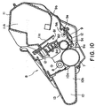
- the developer amount detecting apparatus in this example comprises first and second electrically conductive portions (electrodes) 81 and 82, which are measurement electrodes, and are parts of developer detecting portion 80.
- the electrodes 81 and 82 are disposed along the development roller 9a.
- voltage is applied to the first electrode 81 or the second electrode 82 to induce static electricity between the electrodes 81 and 82, so that the amount of the developer is calculated from the measurement of the amount of the electrostatic capacity between the two electrodes 81 and 82.
- voltage is applied to the first electrode 81. This process will be described later in detail.
- the magnetic developer is attracted to the peripheral surface of the development roller 9a by the magnetic roller 9c contained in the developer roller 9a, and is borne on the peripheral surface of the development roller 9a as the developer 9a is rotated. Then, as the development roller 9a is rotated further, the magnetic developer on the development roller 9a is scraped by the development blade 9d. As a result, an even layer of the magnetic developer is formed on the peripheral surface of the development roller 9a.
- the first and second electrodes 81 and 82 are positioned so that the excessive developer scraped away from the development roller 9a enters between them.
- the first electrode 81 was formed of nonmagnetic SUS, and was 14 mm in width (W1), and 0.3 mm in thickness (t1).
- the second electrode 82 was formed of nonmagnetic SUS, and was 17 mm in width (W2), and 0.5 mm in thickness (t2)- Arranging these electrodes along and in parallel to the development roller 9a in the longitudinal direction produced good results.
- the configurations of the electrodes 81 and 82 need not be limited to particular one. However, arranging the electrodes 81 and 82 non-parallel so that the gap between the two electrodes becomes wider on the side from which the developer enters than on the inward side 85, as shown in Figure 3, provides good results.
- the electrodes 81 and 82 may be formed on a corrugated, or embossed sheet of material, as shown in Figure 8. If it is impossible to secure a space for larger electrodes, because of design related reasons, or if it is desired to reduce the cost, either the first electrode 81 or the second electrode 82 may be formed in the form of a round rod as illustrated in Figures 9 and 10, which show the examples of such arrangement, and in which the first and second electrodes, respectively, are in the form of a round rod. Although the number of the rod in the examples illustrated in Figures 9 and 10 is singular, it may be plural.
- the developer on the peripheral surface of the development roller 9a is leveled, that is, the excess amount of the developer on the peripheral surface of the development roller 9a is scraped away, and as it is scraped away, it enters between the first and second electrodes 81 and 82, as illustrated in Figure 13.
- the gap is filled with the developer T which enters the gap, as illustrated in Figure 14.
- the development chamber 9A is still full of the developer T. Therefore, once the developer T enters the gap through the entrance 84, that is, the bottom side of the gap between the electrodes 81 and 82, it is blocked by the developer T in the development chamber 9A. Therefore, it does not occur until the amount of the developer T in the development chamber 9A reduces by a substantial amount that the developer T between the electrodes 81 and 82 free falls out of the gap between the two electrodes due to gravity or the like. In other words, when there is a sufficient amount of the developer T in the development chamber 9A, the gap between the first and second electrodes 81 and 82 is filled when the developer T, and therefore, the electrostatic capacity between the two electrodes is high.
- the portion of the developer which has been blocking the entrance (also, exit) 84 moves away from the entrance 84, allowing the developer T between the first and second electrodes 81 and 82 to free fall in the gravity direction due to its own weight.
- Some portion of the developer T which free falls may be attracted to the development roller 9a by the magnetic fore as it falls, whereas the other may simply fall all the way to join the rest of the developer T in the development chamber 9A to be supplied again to the development roller 9a.
- the developer T between the two electrodes is caused to directly return to the peripheral surface of the development roller 9a by the magnetic force.
- the amount of the developer in the development chamber 9A has become small enough to allow the developer between the electrodes 81 and 82 to come out from between them.
- the developer still remains in the development chamber 9A by an amount sufficient to make it necessary for the developer to be scraped away from the development roller 9a by the development blade 9b to be supplied into the gap between the first and second electrodes 81 and 82, and therefore, the amount of the developer between the electrodes 81 and 82 gradually reduces in accordance with the amount of the developer remaining in the development chamber 9A.
- the amount of the developer in the development chamber 9A is determined by measuring the amount of the developer between the first and second electrodes 81 and 82, which can be continuously detected by measuring the eletrostatic capacity between the electrodes 81 and 82.
- the structure configuration adjacent to the electrodes 81 and 82 is such that the gap between the first and second electrodes 81 and 82 is provided with no opening at the inward end 85; the gap is provided with only one opening 84, which serves as the entrance as well as the exit. Therefore, widening the gap between the electrodes 81 and 82, on the side of the developer entrance 84 (also, exit), as described above, is effective to allow the developer to easily enter, or come out from, between the two electrodes.
- the amount of the developer scraped away from the peripheral surface of the development roller 9a by the development blade 9b per unit of time increases because of the increase in the rotational speed of the development roller 9a, or the like, the amount of the developer entering between the first and second electrodes 81 and 82 also increases, and sometimes, the developer becomes packed herein. If this packing occurs, the developer between the electrodes 81 and 82 cannot circulates, and in this situation, the self weight of the developer, and/or the magnetic force, is not large enough to cause the packed developer to free fall from between the two electrodes, and therefore, the electrostatic capacity between the two electrodes 81 and 82 does not change, which makes it impossible to detect the developer amount. This phenomenon is most likely to occur under a highly humid ambience in which it is easier for the developer to absorb moisture.
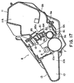
- Figure 17 depicts a structural configuration as a solution to the above described problem of developer packing, according to which an opening 85a, i.e., an exit, is provided, in addition to the opening 84, i.e., the entrance-exit, on the most inward side 85 of the gap between the electrodes 81 and 82, to allow the developer to pass between the electrodes 81 and 82, so that the developer which enters the gap between the two electrodes does not become packed therein.
- an opening 85a i.e., an exit
- the opening 84 i.e., the entrance-exit
- the developer amount detecting portion 80 comprising the first and second electrodes 81 and 82 determines the developer amount by detecting the electrostatic capacity between the two electrodes 81 and 82. Therefore, the positional accuracy of the electrodes is extremely important. Further, since the primary object in this example is to accurately predict the time when toner depletion, which results in various while spots, occurs, the electrodes 81 and 82 should be positioned in the adjacency of the development roller 9a where the developer remains until it is depleted.
- the first and second electrodes 81 and 82 are attached to the development unit frame 12, as shown in Figure 18.
- the means for attaching the first and second electrodes 81 and 82 screws, adhesive, crimping, insert molding, or the like, may be used.
- the electrodes 81 and 82 can be accurately positioned so that the distance between the first and second electrodes 81 and 82 is precisely set. Further, the positioning of the first and second electrodes 81 and 82 in the adjacency of the development roller 9a makes it possible to very closely detect the time when the developer runs out.
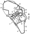
- the process cartridge B design may be modified as shown in Figure 20.
- the second electrode 82 is attached to the development unit frame 12
- the first electrode 81 is attached to the front wall 11a of the developer container 11A, so that the first and second electrodes 81 and 82 oppose each other as the development unit frame 12 is joined with the developer container 11A. This arrangement affords more latitude in terms of the frame structure design for the process cartridge B.
- the contact 19 (unillustrated in Figure 5) disposed in the apparatus main assembly 14 makes electrical contact with the contact portion 93a of the electrical contact 93 of the development roller 9a, and as a result, development bias is applied to the development roller 9a from the bias circuit 101.
- the information obtained by the aforementioned developer amount detecting apparatus is displayed on the monitor screen of a user's personal computer or the like, as shown in Figures 23 and 24; a user is informed of the developer amount by observing the point on a gauge 42 indicated by a hand (needle) 41 which moves in accordance with the developer amount.
- the developer amount detection circuit in this embodiment is provided with a contact 91 to be connected with the electrode 17 of the electrophotographic image forming apparatus main assembly 14 to apply voltage to the first electrode 81, and a contact 93 to be connected with the electrode 19 of the apparatus main assembly 14 to apply the development bias to the development roller 9a.
- the separate provision of these contacts 91 and 93 affords more latitude in design.
- the voltage to be applied to the first electrode 81 is provided from the development bias circuit 101, eliminating the need for an additional power source. Therefore, cost increase can be avoided.
- the contacts are in the form of a single piece, and therefore, there is no stray capacitance, assuring that the electrostatic capacity is accurately measured.
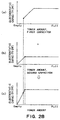
- the developer amount in the process cartridge B is accurately determined by continuously detecting the decrease in the amount of the developer between the electrodes 81 and 82, and the "END" of the developer supply in the process cartridge B is accurately detected by detecting the amount of the developer between the development roller 9a and electrode 83.
- the relationship between the developer amount and the output of the toner amount detection circuit is graphically shown in Figure 28, (a), (b) and (c).
- the developing apparatus C in this example is in the form of a cartridge comprising a developer carrier such as a development roller 9a, a development chamber 9A which contains toner to supply the developer carrier with developer, and a plastic development unit frame 11 in which the developer carrier and development chamber 9A are contained.
- the developing apparatus C a cartridge version of the developing apparatus portion of the process cartridge B in the first example and the embodiment described above, that is, a cartridge formed by eliminating the photosensitive drum 7, charging means 8, and cleaning means 10, from the process cartridge B. Therefore, all the descriptions given to the structures of the developing apparatus portion and developer amount detecting means portion, in the first and second embodiments, also apply to the developing apparatus in this embodiment. Thus, the description of the structure and function of the developing apparatus in this embodiment will be omitted here, by referring to the preceding descriptions of the first example and the embodiment.
- the developing apparatus in this example may be provided with the third electrode 83.
- the amount of the remaining developer can be continuously detected while the amount of the remaining developer is in a range from approximately 30 % down to 0 %, provided that the entire amount of the developer contained in the developer container before a process cartridge is put to use for the first time is 100 %.
- the application of the present invention does not need to be limited to the described embodiment.
- modifications may be made so that the amount of the remaining developer in the developer container can be continuously detected in a range from 50 % down to 0 %, or from 40 % down to 0 %.
Landscapes
- Physics & Mathematics (AREA)
- General Physics & Mathematics (AREA)
- Engineering & Computer Science (AREA)
- Computer Vision & Pattern Recognition (AREA)
- Dry Development In Electrophotography (AREA)
- Electrophotography Configuration And Component (AREA)
Claims (22)
- Dispositif de développement (9) destiné à développer une image latente électrostatique formée sur un élément photosensible électrophotographique (7), ledit dispositif de développement pouvant être monté sur un ensemble principal (14) d'un appareil électrophotographique de formation d'images, ledit dispositif de développement comportant :un élément (9a) de transport de développateur destiné à amener un développateur audit élément photosensible électrophotographique afin de développer l'image latente électrostatique formée sur l'élément photosensible électrophotographique ;une première partie électroconductrice (81) ;une deuxième partie électroconductrice (82) destinée à coopérer avec ladite première partie électroconductrice pour établir une capacité électrostatique, ladite première partie électroconductrice et ladite deuxième partie électroconductrice étant disposées de façon que le développateur puisse entrer entre elles ;un premier contact électrique (91) destiné à recevoir une tension devant être appliquée à ladite première partie électroconductrice depuis l'ensemble principal de l'appareil électrophotographique de formation d'images ;un contact électrique (93) de l'élément de transport de développateur destiné à recevoir une tension devant être appliquée audit élément de transport de développateur depuis l'ensemble principal de l'appareil de formation d'images ;une troisième partie électroconductrice (83) destinée à coopérer avec ledit élément (9a) de transport de développateur pour établir une capacité électrostatique lorsqu'une tension est appliquée audit élément de transport de développateur depuis l'ensemble principal dudit appareil électrophotographique de formation d'images ;un second contact électrique (92) pour la transmission, à l'ensemble principal de l'appareil électrophotographique de formation d'images, d'un signal électrique combiné pour permettre à l'ensemble principal de l'appareil de formation d'images de détecter la quantité restante du développateur, le signal électrique combiné étant formé deun signal électrique correspondant à une capacité électrostatique entre ladite première partie électroconductrice (81) et ladite deuxième partie électroconductrice (82) lorsqu'une tension est appliquée à ladite première partie électroconductrice par l'intermédiaire dudit premier contact électrique (91), etun signal électrique correspondant à une capacité électrostatique entre ledit élément (9a) de transport de développateur et la troisième partie électroconductrice lorsqu'une tension est appliquée audit élément de transport de développateur par l'intermédiaire dudit contact électrique (93) de l'élément de transport de développateur, afin de détecter la quantité restante du développateur dans le dispositif de développement par l'ensemble principal de l'appareil électrophotographique de formation d'images.
- Dispositif de développement selon la revendication 1, dans lequel ladite première partie électroconductrice et ladite deuxième partie électroconductrice sont agencées dans une direction longitudinale d'un élément de transport de développateur sous la forme d'un rouleau de développement, dans lequel ladite première partie électroconductrice est disposée de façon à être plus éloignée dudit élément de transport de développateur que ladite deuxième partie électroconductrice.
- Dispositif de développement selon la revendication 1 ou 2, dans lequel ladite deuxième partie électroconductrice comporte une partie extrême qui est pliée vers ledit élément de transport de développateur, et la capacité électrostatique est établie entre la partie pliée et ledit élément de transport de développateur.
- Dispositif de développement selon la revendication 1, la revendication 2 ou la revendication 3, agencé de manière que le développateur soit amené entre ladite première partie électroconductrice et ladite deuxième partie électroconductrice, et soit rétracté en direction d'un côté d'entrée.
- Dispositif de développement selon la revendication 1, la revendication 2 ou la revendication 3, agencé de manière que le développateur amené entre ladite première partie électroconductrice et ladite deuxième partie électroconductrice passe entre ladite première partie électroconductrice et ladite deuxième partie électroconductrice.
- Dispositif de développement selon la revendication 1, la revendication 2 ou la revendication 3, dans lequel ladite première partie électroconductrice et ladite deuxième partie électroconductrice ont une forme analogue à une plaque plate, et un intervalle entre ladite première partie électroconductrice et ladite deuxième partie électroconductrice est plus large du côté de l'entrée du développateur.
- Dispositif de développement selon la revendication 4, caractérisé en ce qu'il comporte en outre un aimant (9c) disposé dans ledit élément de transport de développateur, et ledit développateur est un développateur magnétique qui est déposé sur la surface dudit élément de transport de développateur.
- Dispositif de développement selon l'une quelconque des revendications 1 à 3, dans lequel ladite troisième partie électroconductrice est constituée d'une seule pièce avec ladite deuxième partie électroconductrice.
- Dispositif de développement selon la revendication 8, dans lequel ladite troisième partie électroconductrice (83) forme un angle par rapport à ladite deuxième partie électroconductrice (82).
- Dispositif de développement selon la revendication 9, dans lequel ladite troisième partie électroconductrice est disposée de façon à être opposée audit élément de transport de développateur, et dans lequel ladite troisième partie électroconductrice est disposée de façon à être plus près dudit élément de transport de développateur que ladite première partie électroconductrice et ladite deuxième partie électroconductrice.
- Cartouche de traitement (B) pouvant être montée de façon amovible sur un ensemble principal (14) d'un appareil électrophotographique de formation d'images, ladite cartouche de traitement comportant :(a) un élément photosensible électrophotographique (7) ; et(b) un dispositif de développement (9) destiné à développer une image latente électrostatique formée sur l'élément photosensible électrophotographique, ledit dispositif de développement comprenant :un élément (9a) de transport de développateur destiné à amener un développateur audit élément photosensible électrophotographique afin de développer l'image latente électrostatique formée sur l'élément photosensible électrophotographique ;une première partie électroconductrice (81) ;une deuxième partie électroconductrice (82) destinée à coopérer avec ladite première partie électroconductrice pour établir une capacité électrostatique, ladite première partie électroconductrice et ladite deuxième partie électroconductrice étant disposées de manière que du développateur puisse entrer entre elles ;un premier contact électrique (91) destiné à recevoir une tension devant être appliquée à ladite première partie électroconductrice depuis l'ensemble principal de l'appareil électrophotographique de formation d'images ;un contact électrique (93) d'élément de transport de développateur destiné à recevoir une tension depuis l'ensemble principal de l'appareil de formation d'images ;une troisième partie électroconductrice (93) destinée à coopérer avec ledit élément (9a) de transport de développateur pour établir une capacité électrostatique lorsqu'une tension est appliquée audit élément de transport de développateur depuis l'ensemble principal dudit appareil électrophotographique de formation d'images ;un second contact électrique (92) destiné à transmettre, à l'ensemble principal de l'appareil électrophotographique de formation d'images, un signal électrique combiné pour permettre à l'ensemble principal de l'appareil de formation d'images de détecter la quantité restante du développateur, le signal électrique combiné étant formé deun signal électrique correspondant à une capacité électrostatique entre ladite première partie électroconductrice (81) et ladite deuxième partie électroconductrice (82) lorsqu'une tension est appliquée à ladite première partie électroconductrice par l'intermédiaire dudit premier contact électrique, etun signal électrique correspondant à une capacité électrostatique entre ledit élément de transport de développateur et la troisième partie électroconductrice lorsqu'une tension est appliquée audit élément de transport de développateur par l'intermédiaire dudit contact électrique de l'élément de transport de développateur, afin de détecter la quantité restante du développateur dans la cartouche de traitement par l'ensemble principal de l'appareil électrophotographique de formation d'images.
- Cartouche de traitement selon la revendication 11, dans laquelle ladite première partie électroconductrice et ladite deuxième partie électroconductrice sont agencées dans une direction longitudinale d'un élément de transport de développateur sous la forme d'un rouleau de développement, et dans laquelle ladite première partie électroconductrice est disposée de façon à être plus éloignée dudit élément de transport de développateur que ladite deuxième partie électroconductrice.
- Cartouche de traitement selon la revendication 11, dans laquelle ladite deuxième partie électroconductrice comporte une partie extrême qui est pliée vers ledit élément de transport de développateur, et la capacité électrostatique est établie entre la partie pliée et ledit élément de transport de développateur.
- Cartouche de traitement selon la revendication 11, la revendication 12 ou la revendication 13, dans laquelle le développateur est amené entre ladite première partie électroconductrice et ladite deuxième partie électroconductrice, et le développateur amené entre ladite première partie électroconductrice et ladite deuxième partie électroconductrice est rétracté en direction d'un côté d'entrée.
- Cartouche de traitement selon la revendication 11, la revendication 12 ou la revendication 13, agencée de manière que le développateur amené entre ladite première partie électroconductrice et ladite deuxième partie électroconductrice passe entre ladite première partie électroconductrice et ladite deuxième partie électroconductrice.
- Cartouche de traitement selon la revendication 11, la revendication 12 ou la revendication 13, dans laquelle ladite première partie électroconductrice et ladite deuxième partie électroconductrice ont une forme analogue à une plaque plate, et l'intervalle entre ladite première partie électroconductrice et ladite deuxième partie électroconductrice est plus large du côté d'entrée du développateur.
- Cartouche de traitement selon la revendication 14, comportant en outre un aimant (9c) disposé dans ledit élément de transport de développateur, et ledit développateur est un développateur magnétique qui est déposé sur la surface dudit élément de transport de développateur.
- Cartouche de traitement selon l'une quelconque des revendications 11 à 13, dans laquelle ladite troisième partie électroconductrice est constituée d'une seule pièce avec ladite deuxième partie électroconductrice.
- Cartouche de traitement selon la revendication 18, dans laquelle ladite troisième partie électroconductrice forme un angle par rapport à ladite deuxième partie électroconductrice.
- Cartouche de traitement selon la revendication 19, dans laquelle ladite troisième partie électroconductrice est disposée de façon à être opposée audit élément de transport de développateur, et dans laquelle ladite troisième partie électroconductrice est disposée de façon à être plus proche dudit élément de transport de développateur que ladite première partie électroconductrice et ladite deuxième partie électroconductrice.
- Appareil électrophotographique de formation d'images destiné à former une image sur un support d'enregistrement, sur lequel une cartouche de traitement (B) peut être montée de façon amovible, ledit appareil comportant :(i) un moyen de montage (16R, 16L) pour le montage de la cartouche de traitement, laquelle comprend :un élément photosensible électrophotographique (7) ; et un dispositif de développement (9) destiné à développer une image latente électrostatique formée sur l'élément photosensible électrophotographique, ledit dispositif de développement comprenant :un élément (9a) de transport de développateur destiné à amener un développateur audit élément photosensible électrophotographique afin de développer l'image latente électrostatique formée sur l'élément photosensible électrophotographique ;une première partie électroconductrice (81) ;une deuxième partie électroconductrice (82) destinée à coopérer avec ladite première partie électroconductrice pour établir une capacité électrostatique, ladite première partie électroconductrice et ladite deuxième partie électroconductrice étant disposées de façon que le développateur puisse entrer entre elles ;un premier contact électrique (91) destiné à recevoir une tension devant être appliquée à ladite première partie électroconductrice depuis l'ensemble principal de l'appareil électrophotographique de formation d'images ;un contact électrique (93) de l'élément de transport de développateur destiné à recevoir une tension devant être appliquée audit élément de transport de développateur depuis l'ensemble principal de l'appareil de formation d'images ;une troisième partie électroconductrice (83) destinée à coopérer avec ledit élément de transport de développateur pour établir une capacité électrostatique lorsqu'une tension est appliquée audit élément de transport de développateur depuis l'ensemble principal dudit appareil électrophotographique de formation d'images ;un second contact électrique (92) destiné à transmettre, à l'ensemble principal de l'appareil électrophotographique de formation d'images, un signal électrique combiné pour permettre à l'ensemble principal de l'appareil de formation d'images de détecter la quantité restante du développateur dans la cartouche de traitement, le signal électrique combiné étant formé deun signal électrique correspondant à une capacité électrostatique entre ladite première partie électroconductrice et ladite deuxième partie électroconductrice lorsqu'une tension est appliquée à ladite première partie électroconductrice par l'intermédiaire dudit premier contact électrique, etun signal électrique correspondant à une capacité électrostatique entre ledit élément de transport de développateur et la troisième partie électroconductrice lorsqu'une tension est appliquée audit élément de transport de développateur par l'intermédiaire dudit contact électrique de l'élément de transport de développateur, afin de détecter la quantité restante du développateur dans la cartouche de traitement par l'ensemble principal de l'appareil électrophotographique de formation d'images ; et(ii) un moyen de détection (80, 100) destiné à détecter sensiblement en temps réel la quantité d'un développateur présente dans ladite cartouche de traitement sur la base du signal électrique transmis depuis ledit second contact électrique.
- Appareil électrophotographique de formation d'images selon la revendication 21, dans lequel ledit moyen de détection de la quantité de développateur est agencé de façon à détecter sensiblement en temps réel la quantité dudit développateur dans ladite cartouche de traitement, et à afficher le résultat de la détection en continu.
Applications Claiming Priority (2)
| Application Number | Priority Date | Filing Date | Title |
|---|---|---|---|
| JP37383498 | 1998-12-28 | ||
| JP37383498 | 1998-12-28 |
Publications (3)
| Publication Number | Publication Date |
|---|---|
| EP1016939A2 EP1016939A2 (fr) | 2000-07-05 |
| EP1016939A3 EP1016939A3 (fr) | 2001-05-30 |
| EP1016939B1 true EP1016939B1 (fr) | 2006-02-01 |
Family
ID=18502839
Family Applications (1)
| Application Number | Title | Priority Date | Filing Date |
|---|---|---|---|
| EP99310455A Expired - Lifetime EP1016939B1 (fr) | 1998-12-28 | 1999-12-22 | Appareil de développement d'une image, unité de traitement, appareil électrophotographique de formation d'images et chassis d'unité de développement |
Country Status (7)
| Country | Link |
|---|---|
| US (2) | US6859627B2 (fr) |
| EP (1) | EP1016939B1 (fr) |
| KR (1) | KR100363808B1 (fr) |
| CN (1) | CN1165818C (fr) |
| AU (1) | AU6553099A (fr) |
| CA (1) | CA2293188C (fr) |
| DE (1) | DE69929667T2 (fr) |
Families Citing this family (34)
| Publication number | Priority date | Publication date | Assignee | Title |
|---|---|---|---|---|
| US6859627B2 (en) * | 1998-12-28 | 2005-02-22 | Canon Kabushiki Kaisha | Image developing apparatus, process cartridge, electrophotographic image forming apparatus, and developing unit frame |
| US6912366B1 (en) * | 1999-08-31 | 2005-06-28 | Canon Kabushiki Kaisha | Image forming apparatus comprising means for detecting an amount of developer contained in a developer container, a memory for storing the amount detected by the detecting means, and control means for updating the information stored in the memory |
| JP3720671B2 (ja) * | 2000-04-06 | 2005-11-30 | キヤノン株式会社 | 現像装置、プロセスカートリッジ、及び電子写真画像形成装置 |
| US6946988B2 (en) * | 2000-11-10 | 2005-09-20 | Simple Devices | Detachable remote controller for an electronic entertainment device and a method for using the same |
| JP3697168B2 (ja) | 2001-03-09 | 2005-09-21 | キヤノン株式会社 | プロセスカートリッジおよび電子写真画像形成装置 |
| US6785479B2 (en) | 2001-12-28 | 2004-08-31 | Canon Kabushiki Kaisha | Image forming apparatus having a control section for detecting an amount of developer and an amount detection method of developer of image forming apparatus |
| JP2003255806A (ja) | 2002-02-28 | 2003-09-10 | Canon Inc | プロセスカートリッジ、現像装置および画像形成装置 |
| JP3848191B2 (ja) * | 2002-03-25 | 2006-11-22 | キヤノン株式会社 | 現像装置およびプロセスカートリッジおよび電子写真画像形成装置 |
| JP2003302825A (ja) * | 2002-04-09 | 2003-10-24 | Canon Inc | 現像装置及びプロセスカートリッジ及び画像形成装置 |
| JP2004205950A (ja) * | 2002-12-26 | 2004-07-22 | Canon Inc | クリーニング装置、プロセスカートリッジおよび画像形成装置 |
| JP3858875B2 (ja) * | 2003-08-25 | 2006-12-20 | 村田機械株式会社 | 現像器及びそれを備えた画像形成装置 |
| JP4110143B2 (ja) * | 2004-01-30 | 2008-07-02 | キヤノン株式会社 | 電子写真画像形成装置、電子写真画像形成装置に着脱可能なユニット及びプロセスカートリッジ |
| JP4095589B2 (ja) * | 2004-02-27 | 2008-06-04 | キヤノン株式会社 | 電子写真画像形成装置、及びプロセスカートリッジ |
| WO2006071251A2 (fr) * | 2004-04-07 | 2006-07-06 | Tiax Llc | Garrot et procede d'utilisation associe |
| JP4963363B2 (ja) * | 2006-03-01 | 2012-06-27 | キヤノン株式会社 | 画像形成装置及び現像剤残量検出方法 |
| JP4804212B2 (ja) * | 2006-04-19 | 2011-11-02 | キヤノン株式会社 | プロセスカートリッジ及び電子写真画像形成装置及びプロセスカートリッジの生産方法及び再生産方法 |
| US7764887B2 (en) * | 2006-04-26 | 2010-07-27 | Ricoh Company, Limited | Developing device and image forming apparatus |
| CN200941842Y (zh) * | 2006-05-25 | 2007-09-05 | 周光真 | 一种多功能头盔 |
| US7555231B2 (en) * | 2006-09-14 | 2009-06-30 | Lexmark International, Inc. | Capacitive toner level sensor and methods of use |
| JP4667444B2 (ja) | 2006-12-13 | 2011-04-13 | キヤノン株式会社 | 電子写真画像形成装置 |
| JP5506236B2 (ja) | 2009-04-30 | 2014-05-28 | キヤノン株式会社 | カートリッジ、及び電子写真画像形成装置 |
| WO2011074707A1 (fr) | 2009-12-16 | 2011-06-23 | キヤノン株式会社 | Cartouche de traitement, unité de tambour photosensible, unité de développement et dispositif de formation d'image xérographique |
| JP5862165B2 (ja) * | 2011-09-29 | 2016-02-16 | ブラザー工業株式会社 | 画像形成装置 |
| JP5906743B2 (ja) | 2012-01-05 | 2016-04-20 | ブラザー工業株式会社 | 画像形成装置 |
| US9250567B2 (en) | 2013-07-12 | 2016-02-02 | Canon Kabushiki Kaisha | Developer container for detecting developer amount based on capacitance, developing apparatus, process cartridge, and image forming apparatus |
| JP6468747B2 (ja) * | 2013-09-24 | 2019-02-13 | キヤノン株式会社 | 現像剤容器、現像装置、プロセスカートリッジ、および画像形成装置 |
| JP6138181B2 (ja) * | 2014-04-15 | 2017-05-31 | キヤノン株式会社 | 画像形成装置に用いられる樹脂成形品及びカートリッジ、並びに画像形成装置に用いられる可動部材の製造方法及びカートリッジの製造方法 |
| US9535398B2 (en) | 2014-09-04 | 2017-01-03 | Canon Kabushiki Kaisha | Developer cartridge, developing apparatus, process cartridge and image forming apparatus |
| JP6444210B2 (ja) * | 2015-02-23 | 2018-12-26 | キヤノン株式会社 | 現像剤容器、現像装置、プロセスカートリッジ、及び現像剤容器の形成方法、現像装置の形成方法、プロセスカートリッジの形成方法 |
| EP3323067B1 (fr) | 2015-07-13 | 2022-07-06 | Ancestry.com DNA, LLC | Système de détermination d'ethnicité génétique locale |
| JP6855284B2 (ja) | 2017-03-03 | 2021-04-07 | キヤノン株式会社 | カートリッジ及び画像形成装置 |
| US10466617B2 (en) * | 2017-12-19 | 2019-11-05 | Lexmark International, Inc. | Capacitive toner level sensor |
| US10969730B2 (en) | 2019-02-25 | 2021-04-06 | Canon Kabushiki Kaisha | Image forming apparatus and image forming unit |
| JP7205361B2 (ja) * | 2019-04-17 | 2023-01-17 | 株式会社リコー | トナー量検出装置、トナー量検出方法、トナー量検出プログラム |
Family Cites Families (48)
| Publication number | Priority date | Publication date | Assignee | Title |
|---|---|---|---|---|
| US4133453A (en) * | 1975-12-18 | 1979-01-09 | Tokyo Shibaura Electric Co., Ltd. | Toner residual amount detecting device |
| JPS57154268A (en) * | 1981-03-19 | 1982-09-24 | Oki Electric Ind Co Ltd | Detector for remaining amount of developer |
| JPS58126556A (ja) * | 1982-01-23 | 1983-07-28 | Canon Inc | 現像装置 |
| JPH01180379A (ja) * | 1988-01-12 | 1989-07-18 | Nec Corp | プリンタ装置 |
| US5003917A (en) * | 1988-08-12 | 1991-04-02 | Minolta Camera Kabushiki Kaisha | Developing apparatus with image quality control |
| JPH02197880A (ja) * | 1989-01-27 | 1990-08-06 | Canon Inc | 現像剤検出装置 |
| JPH03200989A (ja) * | 1989-10-04 | 1991-09-02 | Canon Inc | 画像形成装置 |
| US5623328A (en) | 1990-04-27 | 1997-04-22 | Canon Kabushiki Kaisha | Process cartridge and image forming system on which process cartridge is mountable |
| US5828928A (en) | 1990-04-27 | 1998-10-27 | Canon Kabushiki Kaisha | Process cartridge mountable in an image forming system and a method for assembling a cleaning device |
| US5294960A (en) | 1990-11-06 | 1994-03-15 | Canon Kabushiki Kaisha | Detachable two-frame process cartridge for an image forming apparatus |
| US5229821A (en) | 1990-11-30 | 1993-07-20 | Canon Kabushiki Kaisha | Process cartridge with toner depletion detection feature and image forming apparatus using the same |
| JP2899123B2 (ja) | 1991-03-20 | 1999-06-02 | キヤノン株式会社 | 帯電部材、帯電装置、この帯電装置を備えた画像形成装置及びこの画像形成装置に着脱可能なプロセスユニット |
| JPH04355477A (ja) * | 1991-05-31 | 1992-12-09 | Canon Inc | 画像形成装置 |
| JP3255175B2 (ja) | 1991-10-03 | 2002-02-12 | キヤノン株式会社 | トナー有無検出装置 |
| EP0543485B1 (fr) | 1991-11-20 | 1997-12-03 | Canon Kabushiki Kaisha | Méthode de fixation d'une feuille de raclage, unité de traitement et appareil de formation d'image |
| US5585895A (en) | 1991-12-19 | 1996-12-17 | Canon Kabushiki Kaisha | Developing device and process cartridge with it |
| JP3005130B2 (ja) | 1992-01-10 | 2000-01-31 | キヤノン株式会社 | 帯電装置及び画像形成装置及びプロセスカートリッジ |
| US5534344A (en) | 1992-01-30 | 1996-07-09 | Canon Kabushiki Kaisha | Charging member having a loosely supported charger portion |
| JP3126532B2 (ja) | 1992-02-10 | 2001-01-22 | キヤノン株式会社 | クリーニング装置及びプロセスカートリッジ及び画像形成装置 |
| EP0586044B1 (fr) | 1992-09-04 | 1997-03-26 | Canon Kabushiki Kaisha | Unité de traitement, procédé d'assemblage de cette unité et appareil de formation d'images |
| MX9303563A (es) | 1992-09-04 | 1994-03-31 | Canon Kk | Cartucho de proceso, metodo para ensamblar un cartucho de proceso y aparato formador de imagen. |
| EP0586042B1 (fr) | 1992-09-04 | 1998-09-02 | Canon Kabushiki Kaisha | Unité de traitement et appareil de formation d'images |
| JP3259985B2 (ja) | 1992-09-04 | 2002-02-25 | キヤノン株式会社 | プロセスカートリッジ及び画像形成装置 |
| JPH06161242A (ja) * | 1992-11-17 | 1994-06-07 | Canon Inc | 現像装置 |
| US5966566A (en) | 1993-03-24 | 1999-10-12 | Canon Kabushiki Kaisha | Recycle method for process cartridge and image forming apparatus |
| EP0840176B1 (fr) | 1993-07-30 | 2001-10-31 | Canon Kabushiki Kaisha | Membre de charge, dispositif de charge et cartouche de traitement montée de manière amovible dans un appareil de formation d'images |
| CA2128676C (fr) | 1993-09-08 | 1997-12-23 | John D. Sotack | Capteur volumetrique |
| JPH08179625A (ja) | 1994-12-21 | 1996-07-12 | Canon Inc | プロセスカートリッジ及び画像形成装置 |
| JP3774488B2 (ja) | 1995-04-28 | 2006-05-17 | キヤノン株式会社 | プロセスカートリッジ及び画像形成装置 |
| US5943528A (en) | 1995-04-28 | 1999-08-24 | Canon Kabushiki Kaisha | Toner accommodating container with a gripping cover feature usable with a process cartridge, a process cartridge using the same, and an apparatus using the process cartridge |
| JP3154642B2 (ja) | 1995-04-28 | 2001-04-09 | キヤノン株式会社 | プロセスカートリッジ、トナー現像枠体とクリーニング枠体の結合方法、及び、画像形成装置 |
| JP3268162B2 (ja) | 1995-04-28 | 2002-03-25 | キヤノン株式会社 | プロセスカートリッジ及び画像形成装置 |
| JP3294465B2 (ja) | 1995-04-28 | 2002-06-24 | キヤノン株式会社 | プロセスカートリッジ及び画像形成装置 |
| JPH0916056A (ja) | 1995-06-30 | 1997-01-17 | Canon Inc | プロセスカートリッジ及び画像形成装置 |
| JP3372719B2 (ja) | 1995-07-11 | 2003-02-04 | キヤノン株式会社 | プロセスカートリッジ及び画像形成装置 |
| US5768658A (en) | 1995-07-21 | 1998-06-16 | Canon Kabushiki Kaisha | Electrode member, developing apparatus, process cartridge and image forming apparatus |
| US5768660A (en) | 1995-08-02 | 1998-06-16 | Canon Kabushiki Kaisha | Charging device and process cartridge |
| JP3445040B2 (ja) * | 1995-10-09 | 2003-09-08 | キヤノン株式会社 | 画像形成装置 |
| JP3869877B2 (ja) | 1996-01-09 | 2007-01-17 | キヤノン株式会社 | 電子写真画像形成装置、プロセスカートリッジ及び現像装置 |
| JPH09211960A (ja) * | 1996-01-29 | 1997-08-15 | Canon Inc | プロセスカートリッジ及び画像形成装置 |
| JP3372747B2 (ja) | 1996-02-09 | 2003-02-04 | キヤノン株式会社 | 現像装置 |
| JP3382465B2 (ja) * | 1996-07-04 | 2003-03-04 | キヤノン株式会社 | プロセスカートリッジ及び電子写真画像形成装置 |
| JP3323749B2 (ja) | 1996-08-01 | 2002-09-09 | キヤノン株式会社 | 磁気シール装置及び現像装置並びに画像形成装置 |
| JP3563893B2 (ja) * | 1996-10-30 | 2004-09-08 | キヤノン株式会社 | 画像形成装置及びカートリッジ |
| US5987269A (en) * | 1998-02-13 | 1999-11-16 | Hewlett-Packard Company | Toner quantity measuring technique in an electrophotographic printer |
| JP3530751B2 (ja) * | 1998-10-09 | 2004-05-24 | キヤノン株式会社 | プロセスカートリッジ及び電子写真画像形成装置 |
| JP3530752B2 (ja) * | 1998-10-09 | 2004-05-24 | キヤノン株式会社 | 電子写真画像形成装置、プロセスカートリッジ、現像装置、現像剤供給容器及び測定部品 |
| US6859627B2 (en) * | 1998-12-28 | 2005-02-22 | Canon Kabushiki Kaisha | Image developing apparatus, process cartridge, electrophotographic image forming apparatus, and developing unit frame |
-
1999
- 1999-12-22 US US09/469,517 patent/US6859627B2/en not_active Expired - Lifetime
- 1999-12-22 EP EP99310455A patent/EP1016939B1/fr not_active Expired - Lifetime
- 1999-12-22 DE DE69929667T patent/DE69929667T2/de not_active Expired - Lifetime
- 1999-12-24 AU AU65530/99A patent/AU6553099A/en not_active Abandoned
- 1999-12-24 CA CA002293188A patent/CA2293188C/fr not_active Expired - Fee Related
- 1999-12-28 CN CNB991229916A patent/CN1165818C/zh not_active Expired - Lifetime
- 1999-12-28 KR KR1019990063214A patent/KR100363808B1/ko not_active Expired - Fee Related
-
2004
- 2004-09-07 US US10/934,416 patent/US7095967B2/en not_active Expired - Fee Related
Also Published As
| Publication number | Publication date |
|---|---|
| DE69929667T2 (de) | 2006-08-10 |
| US20050025508A1 (en) | 2005-02-03 |
| CA2293188A1 (fr) | 2000-06-28 |
| CN1267842A (zh) | 2000-09-27 |
| CN1165818C (zh) | 2004-09-08 |
| US6859627B2 (en) | 2005-02-22 |
| DE69929667D1 (de) | 2006-04-13 |
| KR100363808B1 (ko) | 2002-12-11 |
| EP1016939A2 (fr) | 2000-07-05 |
| EP1016939A3 (fr) | 2001-05-30 |
| AU6553099A (en) | 2000-07-20 |
| US7095967B2 (en) | 2006-08-22 |
| KR20000057109A (ko) | 2000-09-15 |
| US20020012542A1 (en) | 2002-01-31 |
| CA2293188C (fr) | 2002-12-10 |
Similar Documents
| Publication | Publication Date | Title |
|---|---|---|
| EP1016939B1 (fr) | Appareil de développement d'une image, unité de traitement, appareil électrophotographique de formation d'images et chassis d'unité de développement | |
| US6804475B2 (en) | Process cartridge comprising grounding, charging bias, and developing bias contacts and input and output contacts, and electrophotographic image forming apparatus to which the process cartridge is detachably mountable | |
| US6892035B2 (en) | Developing device, a process cartridge, and an electrophotographic image forming apparatus for detecting an amount of developer | |
| KR100630988B1 (ko) | 전자 사진식 화상 형성 장치, 프로세스 카트리지, 현상 장치, 현상제 공급 용기 및 이를 위한 측정부 | |
| CA2285157C (fr) | Dispositif de formation d'images electrophotographiques, cartouche pour execution du processus, dispositif de developpement et element de mesure | |
| EP1117015B1 (fr) | Unité de traitement et appareil de formation d'images | |
| JP3848191B2 (ja) | 現像装置およびプロセスカートリッジおよび電子写真画像形成装置 | |
| JP2001092335A (ja) | プロセスカートリッジ、電子写真画像形成装置及び現像剤量検出部材 | |
| EP1083464A2 (fr) | Appareil de développement, unité de traitement, élément d'alimentation et feuille élastique | |
| JP3897504B2 (ja) | 現像装置、プロセスカートリッジ及び電子写真画像形成装置 | |
| JP3984759B2 (ja) | 現像装置、プロセスカートリッジ及び電子写真画像形成装置 | |
| AU782688B2 (en) | Image developing apparatus, process cartridge, electrophotographic image forming apparatus, and development unit frame | |
| JP2001117344A (ja) | 現像装置、プロセスカートリッジ、電子写真画像形成装置及び現像枠体 | |
| JP2003195619A (ja) | 現像装置、プロセスカートリッジおよび画像形成装置 | |
| JP2005121762A (ja) | 現像装置およびプロセスカートリッジおよび電子写真画像形成装置 | |
| JP2001125463A (ja) | プロセスカートリッジ、電子写真画像形成装置、現像装置、現像剤量検出装置及び現像剤残量検出部材 | |
| JP2001125378A (ja) | 現像装置、プロセスカートリッジ及び電子写真画像形成装置 |
Legal Events
| Date | Code | Title | Description |
|---|---|---|---|
| PUAI | Public reference made under article 153(3) epc to a published international application that has entered the european phase |
Free format text: ORIGINAL CODE: 0009012 |
|
| AK | Designated contracting states |
Kind code of ref document: A2 Designated state(s): CH DE FR GB IT LI |
|
| AX | Request for extension of the european patent |
Free format text: AL;LT;LV;MK;RO;SI |
|
| PUAL | Search report despatched |
Free format text: ORIGINAL CODE: 0009013 |
|
| AK | Designated contracting states |
Kind code of ref document: A3 Designated state(s): AT BE CH CY DE DK ES FI FR GB GR IE IT LI LU MC NL PT SE |
|
| AX | Request for extension of the european patent |
Free format text: AL;LT;LV;MK;RO;SI |
|
| 17P | Request for examination filed |
Effective date: 20011015 |
|
| AKX | Designation fees paid |
Free format text: CH DE FR GB IT LI |
|
| 17Q | First examination report despatched |
Effective date: 20040302 |
|
| GRAP | Despatch of communication of intention to grant a patent |
Free format text: ORIGINAL CODE: EPIDOSNIGR1 |
|
| GRAS | Grant fee paid |
Free format text: ORIGINAL CODE: EPIDOSNIGR3 |
|
| GRAA | (expected) grant |
Free format text: ORIGINAL CODE: 0009210 |
|
| AK | Designated contracting states |
Kind code of ref document: B1 Designated state(s): CH DE FR GB IT LI |
|
| PG25 | Lapsed in a contracting state [announced via postgrant information from national office to epo] |
Ref country code: LI Free format text: LAPSE BECAUSE OF FAILURE TO SUBMIT A TRANSLATION OF THE DESCRIPTION OR TO PAY THE FEE WITHIN THE PRESCRIBED TIME-LIMIT Effective date: 20060201 Ref country code: IT Free format text: LAPSE BECAUSE OF FAILURE TO SUBMIT A TRANSLATION OF THE DESCRIPTION OR TO PAY THE FEE WITHIN THE PRESCRIBED TIME-LIMIT;WARNING: LAPSES OF ITALIAN PATENTS WITH EFFECTIVE DATE BEFORE 2007 MAY HAVE OCCURRED AT ANY TIME BEFORE 2007. THE CORRECT EFFECTIVE DATE MAY BE DIFFERENT FROM THE ONE RECORDED. Effective date: 20060201 Ref country code: CH Free format text: LAPSE BECAUSE OF FAILURE TO SUBMIT A TRANSLATION OF THE DESCRIPTION OR TO PAY THE FEE WITHIN THE PRESCRIBED TIME-LIMIT Effective date: 20060201 |
|
| REG | Reference to a national code |
Ref country code: GB Ref legal event code: FG4D |
|
| REG | Reference to a national code |
Ref country code: CH Ref legal event code: EP |
|
| REF | Corresponds to: |
Ref document number: 69929667 Country of ref document: DE Date of ref document: 20060413 Kind code of ref document: P |
|
| REG | Reference to a national code |
Ref country code: CH Ref legal event code: PL |
|
| ET | Fr: translation filed | ||
| PLBE | No opposition filed within time limit |
Free format text: ORIGINAL CODE: 0009261 |
|
| STAA | Information on the status of an ep patent application or granted ep patent |
Free format text: STATUS: NO OPPOSITION FILED WITHIN TIME LIMIT |
|
| 26N | No opposition filed |
Effective date: 20061103 |
|
| PGFP | Annual fee paid to national office [announced via postgrant information from national office to epo] |
Ref country code: FR Payment date: 20131227 Year of fee payment: 15 |
|
| REG | Reference to a national code |
Ref country code: FR Ref legal event code: ST Effective date: 20150831 |
|
| PG25 | Lapsed in a contracting state [announced via postgrant information from national office to epo] |
Ref country code: FR Free format text: LAPSE BECAUSE OF NON-PAYMENT OF DUE FEES Effective date: 20141231 |
|
| PGFP | Annual fee paid to national office [announced via postgrant information from national office to epo] |
Ref country code: GB Payment date: 20181221 Year of fee payment: 20 |
|
| PGFP | Annual fee paid to national office [announced via postgrant information from national office to epo] |
Ref country code: DE Payment date: 20190228 Year of fee payment: 20 |
|
| REG | Reference to a national code |
Ref country code: DE Ref legal event code: R071 Ref document number: 69929667 Country of ref document: DE |
|
| REG | Reference to a national code |
Ref country code: GB Ref legal event code: PE20 Expiry date: 20191221 |
|
| PG25 | Lapsed in a contracting state [announced via postgrant information from national office to epo] |
Ref country code: GB Free format text: LAPSE BECAUSE OF EXPIRATION OF PROTECTION Effective date: 20191221 |