EP1017136A1 - Steckverbinder mit vorgespannten Kontakten und seinem Gebrauch - Google Patents
Steckverbinder mit vorgespannten Kontakten und seinem Gebrauch Download PDFInfo
- Publication number
- EP1017136A1 EP1017136A1 EP99403083A EP99403083A EP1017136A1 EP 1017136 A1 EP1017136 A1 EP 1017136A1 EP 99403083 A EP99403083 A EP 99403083A EP 99403083 A EP99403083 A EP 99403083A EP 1017136 A1 EP1017136 A1 EP 1017136A1
- Authority
- EP
- European Patent Office
- Prior art keywords
- insulating structure
- connector
- solder type
- type contact
- plane
- Prior art date
- Legal status (The legal status is an assumption and is not a legal conclusion. Google has not performed a legal analysis and makes no representation as to the accuracy of the status listed.)
- Granted
Links
- 229910000679 solder Inorganic materials 0.000 claims description 45
- 210000003371 toe Anatomy 0.000 claims description 11
- PXHVJJICTQNCMI-UHFFFAOYSA-N Nickel Chemical compound [Ni] PXHVJJICTQNCMI-UHFFFAOYSA-N 0.000 claims description 6
- 229910000906 Bronze Inorganic materials 0.000 claims description 4
- 239000010974 bronze Substances 0.000 claims description 4
- KUNSUQLRTQLHQQ-UHFFFAOYSA-N copper tin Chemical compound [Cu].[Sn] KUNSUQLRTQLHQQ-UHFFFAOYSA-N 0.000 claims description 4
- PCHJSUWPFVWCPO-UHFFFAOYSA-N gold Chemical compound [Au] PCHJSUWPFVWCPO-UHFFFAOYSA-N 0.000 claims description 3
- 239000010931 gold Substances 0.000 claims description 3
- 229910052737 gold Inorganic materials 0.000 claims description 3
- 239000012212 insulator Substances 0.000 claims description 3
- 229910052759 nickel Inorganic materials 0.000 claims description 3
- 229920001169 thermoplastic Polymers 0.000 claims description 3
- 239000004416 thermosoftening plastic Substances 0.000 claims description 3
- 229910001174 tin-lead alloy Inorganic materials 0.000 claims description 2
- 238000003780 insertion Methods 0.000 description 10
- 230000037431 insertion Effects 0.000 description 10
- 230000000694 effects Effects 0.000 description 6
- 238000000465 moulding Methods 0.000 description 4
- 239000000463 material Substances 0.000 description 3
- 239000002184 metal Substances 0.000 description 2
- 229910052751 metal Inorganic materials 0.000 description 2
- 238000000034 method Methods 0.000 description 2
- 238000005476 soldering Methods 0.000 description 2
- 238000005452 bending Methods 0.000 description 1
- 230000005540 biological transmission Effects 0.000 description 1
- 239000011248 coating agent Substances 0.000 description 1
- 238000000576 coating method Methods 0.000 description 1
- 230000002950 deficient Effects 0.000 description 1
- 239000006185 dispersion Substances 0.000 description 1
- 230000005489 elastic deformation Effects 0.000 description 1
- 239000013013 elastic material Substances 0.000 description 1
- 239000011810 insulating material Substances 0.000 description 1
- LQBJWKCYZGMFEV-UHFFFAOYSA-N lead tin Chemical compound [Sn].[Pb] LQBJWKCYZGMFEV-UHFFFAOYSA-N 0.000 description 1
- 230000035515 penetration Effects 0.000 description 1
- 230000002040 relaxant effect Effects 0.000 description 1
- 238000004381 surface treatment Methods 0.000 description 1
Images
Classifications
-
- H—ELECTRICITY
- H01—ELECTRIC ELEMENTS
- H01R—ELECTRICALLY-CONDUCTIVE CONNECTIONS; STRUCTURAL ASSOCIATIONS OF A PLURALITY OF MUTUALLY-INSULATED ELECTRICAL CONNECTING ELEMENTS; COUPLING DEVICES; CURRENT COLLECTORS
- H01R13/00—Details of coupling devices of the kinds covered by groups H01R12/70 or H01R24/00 - H01R33/00
- H01R13/02—Contact members
- H01R13/22—Contacts for co-operating by abutting
- H01R13/24—Contacts for co-operating by abutting resilient; resiliently-mounted
- H01R13/2442—Contacts for co-operating by abutting resilient; resiliently-mounted with a single cantilevered beam
-
- H—ELECTRICITY
- H01—ELECTRIC ELEMENTS
- H01R—ELECTRICALLY-CONDUCTIVE CONNECTIONS; STRUCTURAL ASSOCIATIONS OF A PLURALITY OF MUTUALLY-INSULATED ELECTRICAL CONNECTING ELEMENTS; COUPLING DEVICES; CURRENT COLLECTORS
- H01R12/00—Structural associations of a plurality of mutually-insulated electrical connecting elements, specially adapted for printed circuits, e.g. printed circuit boards [PCB], flat or ribbon cables, or like generally planar structures, e.g. terminal strips, terminal blocks; Coupling devices specially adapted for printed circuits, flat or ribbon cables, or like generally planar structures; Terminals specially adapted for contact with, or insertion into, printed circuits, flat or ribbon cables, or like generally planar structures
- H01R12/70—Coupling devices
- H01R12/71—Coupling devices for rigid printing circuits or like structures
- H01R12/712—Coupling devices for rigid printing circuits or like structures co-operating with the surface of the printed circuit or with a coupling device exclusively provided on the surface of the printed circuit
- H01R12/714—Coupling devices for rigid printing circuits or like structures co-operating with the surface of the printed circuit or with a coupling device exclusively provided on the surface of the printed circuit with contacts abutting directly the printed circuit; Button contacts therefore provided on the printed circuit
Definitions
- An object of the present invention is a connector with prestressed contacts and the use of this connector.
- a connector of this kind has elastic conductive tabs provided with solder type contact leads and an insulating structure in which the elastic conductive tabs take support. It can be used especially in the mounting of connectors on a printed circuit, especially in the surface-mounting of connectors designed to provide for electrical connection between microcircuits of a chip card and electronic systems. These electronic systems, in a preferred example, are those of chip-card readers or mobile telephones.
- This type of connector comprises elastic conductive tabs designed to provide for electrical contacts by pressure with metal surfaces or contact zones present on the chip card.
- the contact between the solder type contact leads of the connector and the surface of the printed circuit on which these leads have to be soldered must be a flat contact.
- the value of the invention lies in the improvement of the coplaneity of the electrical contact between any solder type contact lead and the surface of the printed circuit.
- the presently manufactured connectors designed for surface mounting comprise solder type contact leads whose free end is cambered to form a contact plane with the printed circuit.
- Each solder type contact lead defines a local contact plane designed to come into contact with the printed circuit.
- the local contact planes taken together, define a distribution, along the thickness, of the connector contacts with respect to the plane of the printed circuit.
- the cambering of the elastic conductive tabs is done according to methods that cannot be used to easily obtain high repeatability with regard to the coplaneity of the solder type contact leads (in surface mounting). This means that, between two elastic conductive tabs, there may be substantial differences in shape and/or dimension. Firstly, it may happen that a solder type contact lead of a tab is not perfectly plane. Secondly, two solder type contact leads, each of which may be plane, may have contact planes that are different and/or are not parallel with one another.
- this type of connector consists of a thermoplastic insulating structure and a certain number of bronze contacts, six in one example. These contacts are treated and receive a triple coating of nickel, then tin-lead allow and finally a thin layer of gold for the part in contact with the chip card.
- the leads of these contacts are designed to be surface mounted on a printed circuit.
- a chip card connector belonging for example to a mobile telephone or to another electronic system that may undergo vibrations will transmit these vibrations to the chip card as well as to the connector.
- a reduction of the contact pressure on the chip card will cause problems because, if a vibration is excessive, a contact between the chip card and the connector may be interrupted or defective even for a short instant. This may lead to errors in the reading and writing of information in the chip card.
- lead-outs of the components namely the solder type contact leads, must be designed to ensure coplaneity of less than 0.1 mm.
- This in fact entails a dimension X, representing a distance between the supporting face of the insulator of the component and the soldering face of the CMS lead-outs, whose tolerance interval is 0.1 mm (X ⁇ 0.05 mm).
- This dimension X results from a double cambering of an elastic conductive tab (the contact zone with the chip card has to be elastic) and it is the elasticity of this elastic conductive tab that is the cause of most of the problems encountered, especially those defined here above.
- This elasticity varies as a function of the material used to make an elastic conductive tab, its thickness or again the surface treatment applied. Thus, there are too many parameters at play to be sure of obtaining large batches of elastic conducive tabs with a tolerance of plus or minus 0.05 millimetres.
- the insulating structure comprises stops aligned in a plane.
- the solder type contact leads press on these stops in this plane by the effect of a prestress applied to them.
- the contact surface of the solder type contact leads is placed against the plane of the stops with a precision of about 0.02 mm, it being known that it is possible to mould insulator materials with a precision of this degree. Consequently, the contact between the solder type contact leads of the connector and the surface of the printed circuit is a perfectly plane contact.
- the contact zones of the elastic tabs with a chip card are also in a plane that is perfectly parallel to the contact plane of the chip card.
- the invention therefore relates to a connector comprising an insulating structure and a plurality of elastic conductive tabs, held in this insulating structure, each elastic conductive tab being provided with a solder type contact lead wherein the solder type contact leads are prestressed and the insulating structure comprises stops aligned in a plane on which the prestressed contact leads apply pressure.
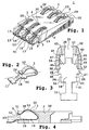
- FIG. 1 shows a connector 1 according to the invention.
- This connector 1 comprises an insulating structure 2 and, in a preferred example, six elastic conductive tabs 3 to 8. They are distributed in groups of three, symmetrically and evenly, along two sides 9 and 10 of the insulating structure 2, these two sides 9 and 10 being opposite.
- the description shall be limited to the elements located on the side 9, the elements of the side 10 being deduced from the side 9 by symmetry.
- solder type contact leads 11, 12, 13 are provided with solder type contact leads 11, 12, 13 respectively.
- these solder type contact leads are in the form of flat plates located at first ends of the tabs 3, 4 and 5 respectively.
- the solder type contact leads 11, 12 and 13 are positioned perpendicularly to the side 9 of the insulating structure 2.
- the insulating structure 2 comprises stops 14, 15, 16 and 17, evenly aligned in a plane. This plane is perpendicular to the side 9.
- the solder type contact leads 11, 12, 13 have a T-shaped widening. These T-shaped widenings, from the solder type contact leads 11, 12, 13 press on stops 14, 15, 16 and 17. To do this, each solder type contact lead is located between two stops.
- the stops 14 to 17 are structures that rise perpendicularly to the side 9 and have at least one plane face. These plane faces are those beneath which the solder type contact leads press. These stops are rigid so that pressures applied by the solder type contact leads are not enough to deform the supporting planes of the stops. Thus, the widenings of the solder type contact lead 11 press on two stops 14 and 15, the solder type contact lead 12 presses on two stops 15 and 16 and so on and so forth.
- the plane of the stops 14 to 17 is by design (moulding) obtained within the desired tolerance.
- Figure 2 shows the conducive elastic tab 3 outside the connector 1. It comprises an anchor plate 18 placed in an intermediate position.
- This intermediate position is a position in which the anchor plate 18 is closer to the end comprising the solder type contact lead 11 than the other end of the elastic conductive tab 3.
- This anchor plate 18 is forcefully inserted into a housing 19 designed for this purpose in the insulating structure 2.
- the insulating structure 2 has as many housings as it has elastic conductive tabs. In the example shown, the insulating structure 2 therefore has six housings 19 to 24.
- This forceful insertion of the anchor plate 18 provides for a fixed link between the anchor plate 18 and the insulating structure 2.
- This anchor plate 18 extends laterally with two lateral arms 25 and 26.
- the forceful insertion of the anchor plate 18 into the housing 19 designed for this purpose in the insulating structure 2 has the effect of inserting the two lateral arms 25 and 26 into two lateral grooves made in each housing.
- the contact lead 11 is prestressed so that it gets placed against the stops 14 and 15 once the tab has been inserted.
- the insulating structure 2 is obtained by moulding.
- the moulding methods currently used make it possible to obtain plane surfaces and dimensions with a precision of about 0.02 mm. This means that it is possible to obtain surfaces whose variations in relief are contained in a space whose thickness may be reduced to about 0.02 mm.
- the elastic properties of the tabs are then used. Indeed, when the solder type contact leads press on the stops, the reaction force is sufficient to obtain a deformation of the solder type contact leads in such a way that a contact between a solder type contact lead and a stop will be a plane contact. Thus, the planeity obtained in the invention for the solder type contact leads 11, 12 and 13 is greater than the planeity obtained in the prior art.
- Figure 3 shows the anchor plate 18 provided with two lateral arms 25 and 26. These two fixing arms 25 and 26 are extended, parallel to a plane passing through the anchor plate 18, by two lateral fixing toes 27 and 28 respectively.
- a lateral fixing toe, 27 or 28 has a harpoon shape in which a first flank 29 or 30 is perpendicular to an end 31 or 32 of a lateral arm 25 or 26 respectively.
- a second flank 33 or 34 is oblique to the end 31 or 32 respectively.
- the toes 27 and 28 are positioned in such a way that, with respect to the direction of insertion of the anchor plate 18, it is the oblique flanks 33 and 34 of the toes 27 and 28 that first penetrate the grooves 35 and 36 respectively designed for this purpose in the walls 37 and 38 of a housing 39.
- the flanks 29 and 30 of the toes 27 and 28 penetrate in a second stage.
- the toes 27 and 28 penetrate the walls 40 and 41 of the grooves 35 and 36 respectively facing them.
- the two toes 27 and 28 bend the walls 40 and 41 under the effect of an insertion force applied to the anchor plate 18.
- This bending of the walls 40 and 41 has the effect of producing a compressive stress on the toes 27 and 28 and therefore of fixing the anchor plate 18.
- the anchor plate 18 reaches a position where it abuts the walls 42 and 43 constituting a termination of the grooves 35 and 36 respectively. In this state, the anchor plate 18 can no longer go forward because of the walls 42 and 43. It cannot move sideways because of the compressive stresses applied by the walls 40 and 41 and it cannot return backwards because of the perpendicular flanks 29 and 30 of the toes 25 and 26 which counter any translational movement along this direction of the anchor plate 18.
- the anchor plate 18 is therefore fixed and has no degree of liberty. Furthermore, two front corners 44 and 45 of the anchor plate 18 are bevelled. These two corners 44 and 45 are angles that are formed at the intersection between the ends 31 and 32, of the lateral arms 25 and 26 with sides 46 and 47 respectively. These sides 46 and 47 are those which, at the end of the insertion of the anchor plate 18, come into contact with the walls 42 and 43 of the grooves 35 and 36 respectively. These bevelled corners 39 and 40 further the engagement of the anchor plate 18 in the grooves 35 and 36 respectively.
- Figure 4 shows a section of the connector 1 along a sectional plane passing through the conductive elastic tabs 3 and 8 (the conductive elastic tab 8 is not shown).
- a housing 19 receiving the conductive tab 3 comprises a first aperture on the side 9 of the insulating structure 2 as well as a second aperture on a side 48 perpendicular to the side 9 but parallel to the contact plane of the stop.
- the elastic conductive tab 3 introduced by the side 9 is compressed in the housing 19.
- the elastic conductive tab 3 has a folded-down shape and a second end 49 that is in a plane parallel to but not the same as the plane passing through the anchor plate 18.
- a part of the elastic conductive tab 3, located between the end 49 and the anchor plate 18, is cambered in such a way that a piece of this part opens into the second aperture of the side 48 with a humped shape 50. It is this position of the elastic conductive tab 3 that is designed to form an electrical contact between the chip card and the connector 1. This contact zone of the hump 50 with the chip card is movable with respect to the anchor plate.
- this cambered shape of this part of the elastic conductive tab 3 makes it possible, when a pressure is applied along an axis perpendicular to the side 48, to obtain a spring effect from this part.
- This spring effect in a preferred example, provides for electrical contact by pressure between the elastic conducive tab 3 and a metal contact zone on the chip card.
- the end 49 of the elastic conductive tab 3 is subjected to a second prestress. For this purpose, it is held, by stops between the walls 37 and 38 of the housing 19, at a height such that a distance between a stop 51, made in the wall 38, and the plane passing through the anchor plate 18 is smaller than the gap between this same plane and the end 49 when it is not subjected to any stress.
- the end 49 therefore cannot move in a housing 52 except in one direction, namely the direction facing the stop 51.
- a T-shaped widening of the end 49 of the elastic conductive tab 3 makes it possible to press on this stop 51.
- This last-mentioned prestress is aimed especially at providing approximately a same contact plane for all the contact zones, this contact plane being parallel to the contact plane of the solder type contact leads.
- the distance between a peak 53 of the hump and the side 48 is such that a penetration of the hump 50 into the housing 19 due to pressure applied by the chip card during the connection always leaves at least the end 53 outside the housing 19.
- the resultant reaction force provides for sufficient mutual facing contact between the contact zones of the connector 1 and the contact zones of the chip card to have electrical contact by pressure according to the criteria explained here above.
- an elastic conductive tab 3 During the insertion of an elastic conductive tab 3 into the housing 19 of the insulating structure 2, a squeezing force needs to be applied between the anchor plate 18 and the end 49. This enables the end 49 to be inserted into the housing 52. After the relaxing of the squeezing force, the end 49 abuts the stop 51. Furthermore, during the insertion, the contact lead 11 of the elastic conductive tab 3 is positioned as defined here above. In this case, the elastic conductive tab 3 is subjected to two prestresses in reaction with the anchor plate 18. The first prestress is that of the solder type contact leads 11, 12 and 13 on the stops 14, 15, 16 and 17. In the example, two stops are used to make a prestress on a solder type contact lead. Thus, each solder type contact lead is between two stops. One consequence of this placing of the solder type contact leads between the stops is that the tabs are no longer mobile. This limits the risks that a fixing tab might get hooked during the mounting operations.
- the insulating structure 2 is made out of a moulding through the use of a thermoplastic insulating material. Materials of this kind have properties of elasticity and deformation used especially during the insertion of the anchor elements of the conductive elastic tabs as explained here above.
- the elastic conductive tabs 3 to 8 in a preferred example, are made of bronze since bronze is an elastic material that is easy to shape. This means that it can be easily deformed. This is one of the aims sought when the contact tabs press on the stops of the insulating structure. The contact tabs thus match the relief features resulting from the stops.
- the humped structure of an elastic conductive tab providing contact with the chip card, is covered with nickel, a tin-lead alloy and/or gold in order to improve the contact characteristics of the elastic conductive tab and thus promote efficient electrical contact between the connector 1 and the chip card.
Landscapes
- Coupling Device And Connection With Printed Circuit (AREA)
- Multi-Conductor Connections (AREA)
Applications Claiming Priority (2)
| Application Number | Priority Date | Filing Date | Title |
|---|---|---|---|
| FR9815618A FR2787245B1 (fr) | 1998-12-10 | 1998-12-10 | Connecteur a contacts precontraints et son utilisation |
| FR9815618 | 1998-12-10 |
Publications (2)
| Publication Number | Publication Date |
|---|---|
| EP1017136A1 true EP1017136A1 (de) | 2000-07-05 |
| EP1017136B1 EP1017136B1 (de) | 2002-09-11 |
Family
ID=9533831
Family Applications (1)
| Application Number | Title | Priority Date | Filing Date |
|---|---|---|---|
| EP99403083A Expired - Lifetime EP1017136B1 (de) | 1998-12-10 | 1999-12-09 | Leiterplattenoberflächenmontierbarer elektrischer Verbinder mit vorgespannten Kontakten |
Country Status (6)
| Country | Link |
|---|---|
| EP (1) | EP1017136B1 (de) |
| JP (1) | JP2000200638A (de) |
| AT (1) | ATE224109T1 (de) |
| CA (1) | CA2291380A1 (de) |
| DE (1) | DE69902865T2 (de) |
| FR (1) | FR2787245B1 (de) |
Cited By (4)
| Publication number | Priority date | Publication date | Assignee | Title |
|---|---|---|---|---|
| FR2816767A1 (fr) * | 2000-11-14 | 2002-05-17 | Fci Pontarlier | Connecteur de carte a puce avec bloc de montage des lames de contact ressorts |
| WO2002056419A3 (en) * | 2000-12-21 | 2002-12-19 | Amphenol Tuchel Elect | A flat contact element for a smart card connector and a smart card connector using a flat contact element |
| ES2383746A1 (es) * | 2004-05-14 | 2012-06-26 | Tyco Electronics Japan G.K. | Conector electrico montado en placa |
| CN120221221A (zh) * | 2025-05-26 | 2025-06-27 | 聚变新能(安徽)有限公司 | 一种接电板、馈电接头、馈电接头保护机构以及真空压力浸渍模具 |
Families Citing this family (7)
| Publication number | Priority date | Publication date | Assignee | Title |
|---|---|---|---|---|
| JP3477640B2 (ja) * | 2000-08-10 | 2003-12-10 | 日本航空電子工業株式会社 | コネクタ |
| JP2002260759A (ja) | 2001-03-05 | 2002-09-13 | Jst Mfg Co Ltd | 横置き電気コネクタ |
| JP3595939B2 (ja) | 2002-03-29 | 2004-12-02 | 日本航空電子工業株式会社 | コネクタ |
| TWI255077B (en) * | 2005-06-27 | 2006-05-11 | Fci Asia Technology Pte Ltd | Housing, terminal and connector using the housing and the terminal |
| JP2009032440A (ja) * | 2007-07-25 | 2009-02-12 | Jst Mfg Co Ltd | 電気コネクタ |
| TWM602744U (zh) * | 2020-01-20 | 2020-10-11 | 唐虞企業股份有限公司 | 受力機構及其構成的連接器 |
| CN216850424U (zh) | 2022-03-18 | 2022-06-28 | 北京小米移动软件有限公司 | 触点模组和电子设备 |
Citations (4)
| Publication number | Priority date | Publication date | Assignee | Title |
|---|---|---|---|---|
| DE9407499U1 (de) * | 1994-05-05 | 1995-09-07 | Itt Composants Et Instruments, Dole Cedex | Elektrisches Kontaktelement |
| WO1996033527A1 (fr) * | 1995-04-21 | 1996-10-24 | Itt Composants Et Instruments | Connecteur electrique, notamment pour le raccordement d'une carte a memoire electronique |
| EP0756355A1 (de) * | 1995-07-28 | 1997-01-29 | Itt Composants Et Instruments | Elektrischer Steckverbinder zur Verbindung mit den Kontakten einer integrierten gedruckten Schaltung |
| WO1998016973A1 (en) * | 1996-10-11 | 1998-04-23 | Bourns, Inc. | Electrical connector assembly |
-
1998
- 1998-12-10 FR FR9815618A patent/FR2787245B1/fr not_active Expired - Fee Related
-
1999
- 1999-12-01 CA CA002291380A patent/CA2291380A1/en not_active Abandoned
- 1999-12-09 EP EP99403083A patent/EP1017136B1/de not_active Expired - Lifetime
- 1999-12-09 DE DE69902865T patent/DE69902865T2/de not_active Expired - Fee Related
- 1999-12-09 AT AT99403083T patent/ATE224109T1/de not_active IP Right Cessation
- 1999-12-10 JP JP11351953A patent/JP2000200638A/ja active Pending
Patent Citations (4)
| Publication number | Priority date | Publication date | Assignee | Title |
|---|---|---|---|---|
| DE9407499U1 (de) * | 1994-05-05 | 1995-09-07 | Itt Composants Et Instruments, Dole Cedex | Elektrisches Kontaktelement |
| WO1996033527A1 (fr) * | 1995-04-21 | 1996-10-24 | Itt Composants Et Instruments | Connecteur electrique, notamment pour le raccordement d'une carte a memoire electronique |
| EP0756355A1 (de) * | 1995-07-28 | 1997-01-29 | Itt Composants Et Instruments | Elektrischer Steckverbinder zur Verbindung mit den Kontakten einer integrierten gedruckten Schaltung |
| WO1998016973A1 (en) * | 1996-10-11 | 1998-04-23 | Bourns, Inc. | Electrical connector assembly |
Cited By (4)
| Publication number | Priority date | Publication date | Assignee | Title |
|---|---|---|---|---|
| FR2816767A1 (fr) * | 2000-11-14 | 2002-05-17 | Fci Pontarlier | Connecteur de carte a puce avec bloc de montage des lames de contact ressorts |
| WO2002056419A3 (en) * | 2000-12-21 | 2002-12-19 | Amphenol Tuchel Elect | A flat contact element for a smart card connector and a smart card connector using a flat contact element |
| ES2383746A1 (es) * | 2004-05-14 | 2012-06-26 | Tyco Electronics Japan G.K. | Conector electrico montado en placa |
| CN120221221A (zh) * | 2025-05-26 | 2025-06-27 | 聚变新能(安徽)有限公司 | 一种接电板、馈电接头、馈电接头保护机构以及真空压力浸渍模具 |
Also Published As
| Publication number | Publication date |
|---|---|
| ATE224109T1 (de) | 2002-09-15 |
| EP1017136B1 (de) | 2002-09-11 |
| DE69902865D1 (de) | 2002-10-17 |
| FR2787245A1 (fr) | 2000-06-16 |
| FR2787245B1 (fr) | 2001-02-23 |
| CA2291380A1 (en) | 2000-06-10 |
| DE69902865T2 (de) | 2003-04-30 |
| JP2000200638A (ja) | 2000-07-18 |
Similar Documents
| Publication | Publication Date | Title |
|---|---|---|
| US7097506B2 (en) | Contact module in which mounting of contacts is simplified | |
| JP2803574B2 (ja) | コネクタのプレスイン端子及びその製造方法 | |
| EP0623248B2 (de) | Elektrischer verbinder mit blech als steckkontaktmaterial | |
| EP1017136B1 (de) | Leiterplattenoberflächenmontierbarer elektrischer Verbinder mit vorgespannten Kontakten | |
| JP3746106B2 (ja) | 基板用電気コネクタ | |
| EP1128477B1 (de) | Elektrischer Verbinder mit Kompressionskontakten | |
| JPH0355779A (ja) | 表面実装型相互接続装置 | |
| US5695353A (en) | Electrical connector | |
| US6830461B2 (en) | Electrical contact and electrical connection device using same | |
| WO2003052877A1 (en) | Interposer assembly for soldered electrical connections | |
| US20010034162A1 (en) | Connector with prestressed contacts and its use | |
| US6508675B1 (en) | Electrical connector configured by wafers including moveable contacts | |
| CN1319218C (zh) | 具有用于接地的连接板的电连接器 | |
| EP0591007B1 (de) | Miniatur Trennstelle | |
| HK35284A (en) | An electrical terminal and an edgecard connector incorporating the same | |
| US20010014559A1 (en) | Electronic component inwhich an insert member is tightly held by a resin portion and prevented from deformation thereof | |
| US6000973A (en) | Electrical connector with plug contact elements of plate material | |
| US6227917B1 (en) | Contact structure for high speed transmission connector | |
| KR100515993B1 (ko) | 전기 커넥터용 접촉자 및 그 접촉자를 구비한 전기커넥터 | |
| US7210225B2 (en) | Methods for controlling contact height | |
| US20030082933A1 (en) | Ball grid array socket | |
| JP2000501225A (ja) | 滑らかなコンタクト端子を形成する方法 | |
| JP2024078870A (ja) | 基板対基板コネクタ | |
| JPS58165282A (ja) | 無はんだ電気接触子 | |
| EP1311032B1 (de) | Steckverbinder hoher Kontaktdichte und Herstellungsverfahren |
Legal Events
| Date | Code | Title | Description |
|---|---|---|---|
| PUAI | Public reference made under article 153(3) epc to a published international application that has entered the european phase |
Free format text: ORIGINAL CODE: 0009012 |
|
| AK | Designated contracting states |
Kind code of ref document: A1 Designated state(s): AT BE CH CY DE DK ES FI FR GB GR IE IT LI LU MC NL PT SE |
|
| AX | Request for extension of the european patent |
Free format text: AL;LT;LV;MK;RO;SI |
|
| 17P | Request for examination filed |
Effective date: 20001114 |
|
| 17Q | First examination report despatched |
Effective date: 20010129 |
|
| AKX | Designation fees paid |
Free format text: AT BE CH CY DE DK ES FI FR GB GR IE IT LI LU MC NL PT SE |
|
| GRAG | Despatch of communication of intention to grant |
Free format text: ORIGINAL CODE: EPIDOS AGRA |
|
| RTI1 | Title (correction) |
Free format text: ELECTRICAL SURFACE MOUNTING CONNECTOR WITH PRESTRESSED CONTACTS |
|
| GRAG | Despatch of communication of intention to grant |
Free format text: ORIGINAL CODE: EPIDOS AGRA |
|
| GRAH | Despatch of communication of intention to grant a patent |
Free format text: ORIGINAL CODE: EPIDOS IGRA |
|
| GRAH | Despatch of communication of intention to grant a patent |
Free format text: ORIGINAL CODE: EPIDOS IGRA |
|
| GRAA | (expected) grant |
Free format text: ORIGINAL CODE: 0009210 |
|
| RAP1 | Party data changed (applicant data changed or rights of an application transferred) |
Owner name: FCI |
|
| AK | Designated contracting states |
Kind code of ref document: B1 Designated state(s): AT BE CH CY DE DK ES FI FR GB GR IE IT LI LU MC NL PT SE |
|
| PG25 | Lapsed in a contracting state [announced via postgrant information from national office to epo] |
Ref country code: NL Free format text: LAPSE BECAUSE OF FAILURE TO SUBMIT A TRANSLATION OF THE DESCRIPTION OR TO PAY THE FEE WITHIN THE PRESCRIBED TIME-LIMIT Effective date: 20020911 Ref country code: LI Free format text: LAPSE BECAUSE OF FAILURE TO SUBMIT A TRANSLATION OF THE DESCRIPTION OR TO PAY THE FEE WITHIN THE PRESCRIBED TIME-LIMIT Effective date: 20020911 Ref country code: IT Free format text: LAPSE BECAUSE OF FAILURE TO SUBMIT A TRANSLATION OF THE DESCRIPTION OR TO PAY THE FEE WITHIN THE PRESCRIBED TIME-LIMIT;WARNING: LAPSES OF ITALIAN PATENTS WITH EFFECTIVE DATE BEFORE 2007 MAY HAVE OCCURRED AT ANY TIME BEFORE 2007. THE CORRECT EFFECTIVE DATE MAY BE DIFFERENT FROM THE ONE RECORDED. Effective date: 20020911 Ref country code: GR Free format text: LAPSE BECAUSE OF FAILURE TO SUBMIT A TRANSLATION OF THE DESCRIPTION OR TO PAY THE FEE WITHIN THE PRESCRIBED TIME-LIMIT Effective date: 20020911 Ref country code: FI Free format text: LAPSE BECAUSE OF FAILURE TO SUBMIT A TRANSLATION OF THE DESCRIPTION OR TO PAY THE FEE WITHIN THE PRESCRIBED TIME-LIMIT Effective date: 20020911 Ref country code: CH Free format text: LAPSE BECAUSE OF FAILURE TO SUBMIT A TRANSLATION OF THE DESCRIPTION OR TO PAY THE FEE WITHIN THE PRESCRIBED TIME-LIMIT Effective date: 20020911 Ref country code: BE Free format text: LAPSE BECAUSE OF FAILURE TO SUBMIT A TRANSLATION OF THE DESCRIPTION OR TO PAY THE FEE WITHIN THE PRESCRIBED TIME-LIMIT Effective date: 20020911 Ref country code: AT Free format text: LAPSE BECAUSE OF FAILURE TO SUBMIT A TRANSLATION OF THE DESCRIPTION OR TO PAY THE FEE WITHIN THE PRESCRIBED TIME-LIMIT Effective date: 20020911 |
|
| REF | Corresponds to: |
Ref document number: 224109 Country of ref document: AT Date of ref document: 20020915 Kind code of ref document: T |
|
| REG | Reference to a national code |
Ref country code: GB Ref legal event code: FG4D |
|
| REG | Reference to a national code |
Ref country code: CH Ref legal event code: EP |
|
| REG | Reference to a national code |
Ref country code: IE Ref legal event code: FG4D |
|
| REF | Corresponds to: |
Ref document number: 69902865 Country of ref document: DE Date of ref document: 20021017 |
|
| ET | Fr: translation filed | ||
| PG25 | Lapsed in a contracting state [announced via postgrant information from national office to epo] |
Ref country code: LU Free format text: LAPSE BECAUSE OF NON-PAYMENT OF DUE FEES Effective date: 20021209 Ref country code: IE Free format text: LAPSE BECAUSE OF NON-PAYMENT OF DUE FEES Effective date: 20021209 |
|
| PG25 | Lapsed in a contracting state [announced via postgrant information from national office to epo] |
Ref country code: SE Free format text: LAPSE BECAUSE OF FAILURE TO SUBMIT A TRANSLATION OF THE DESCRIPTION OR TO PAY THE FEE WITHIN THE PRESCRIBED TIME-LIMIT Effective date: 20021211 Ref country code: DK Free format text: LAPSE BECAUSE OF FAILURE TO SUBMIT A TRANSLATION OF THE DESCRIPTION OR TO PAY THE FEE WITHIN THE PRESCRIBED TIME-LIMIT Effective date: 20021211 |
|
| PG25 | Lapsed in a contracting state [announced via postgrant information from national office to epo] |
Ref country code: PT Free format text: LAPSE BECAUSE OF FAILURE TO SUBMIT A TRANSLATION OF THE DESCRIPTION OR TO PAY THE FEE WITHIN THE PRESCRIBED TIME-LIMIT Effective date: 20021217 |
|
| PG25 | Lapsed in a contracting state [announced via postgrant information from national office to epo] |
Ref country code: CY Free format text: LAPSE BECAUSE OF FAILURE TO SUBMIT A TRANSLATION OF THE DESCRIPTION OR TO PAY THE FEE WITHIN THE PRESCRIBED TIME-LIMIT Effective date: 20021231 |
|
| NLV1 | Nl: lapsed or annulled due to failure to fulfill the requirements of art. 29p and 29m of the patents act | ||
| REG | Reference to a national code |
Ref country code: CH Ref legal event code: PL |
|
| PG25 | Lapsed in a contracting state [announced via postgrant information from national office to epo] |
Ref country code: ES Free format text: LAPSE BECAUSE OF FAILURE TO SUBMIT A TRANSLATION OF THE DESCRIPTION OR TO PAY THE FEE WITHIN THE PRESCRIBED TIME-LIMIT Effective date: 20030328 |
|
| PG25 | Lapsed in a contracting state [announced via postgrant information from national office to epo] |
Ref country code: MC Free format text: LAPSE BECAUSE OF NON-PAYMENT OF DUE FEES Effective date: 20030701 |
|
| PLBE | No opposition filed within time limit |
Free format text: ORIGINAL CODE: 0009261 |
|
| STAA | Information on the status of an ep patent application or granted ep patent |
Free format text: STATUS: NO OPPOSITION FILED WITHIN TIME LIMIT |
|
| 26N | No opposition filed |
Effective date: 20030612 |
|
| REG | Reference to a national code |
Ref country code: IE Ref legal event code: MM4A |
|
| PGFP | Annual fee paid to national office [announced via postgrant information from national office to epo] |
Ref country code: GB Payment date: 20051104 Year of fee payment: 7 |
|
| GBPC | Gb: european patent ceased through non-payment of renewal fee |
Effective date: 20061209 |
|
| PG25 | Lapsed in a contracting state [announced via postgrant information from national office to epo] |
Ref country code: GB Free format text: LAPSE BECAUSE OF NON-PAYMENT OF DUE FEES Effective date: 20061209 |
|
| PGFP | Annual fee paid to national office [announced via postgrant information from national office to epo] |
Ref country code: DE Payment date: 20071228 Year of fee payment: 9 |
|
| PGFP | Annual fee paid to national office [announced via postgrant information from national office to epo] |
Ref country code: FR Payment date: 20071204 Year of fee payment: 9 |
|
| REG | Reference to a national code |
Ref country code: FR Ref legal event code: ST Effective date: 20090831 |
|
| PG25 | Lapsed in a contracting state [announced via postgrant information from national office to epo] |
Ref country code: DE Free format text: LAPSE BECAUSE OF NON-PAYMENT OF DUE FEES Effective date: 20090701 |
|
| PG25 | Lapsed in a contracting state [announced via postgrant information from national office to epo] |
Ref country code: FR Free format text: LAPSE BECAUSE OF NON-PAYMENT OF DUE FEES Effective date: 20081231 |