EP1017156A1 - Dispositif de circuit pour commander une charge électrique à courant alternatif - Google Patents
Dispositif de circuit pour commander une charge électrique à courant alternatif Download PDFInfo
- Publication number
- EP1017156A1 EP1017156A1 EP98830809A EP98830809A EP1017156A1 EP 1017156 A1 EP1017156 A1 EP 1017156A1 EP 98830809 A EP98830809 A EP 98830809A EP 98830809 A EP98830809 A EP 98830809A EP 1017156 A1 EP1017156 A1 EP 1017156A1
- Authority
- EP
- European Patent Office
- Prior art keywords
- electric load
- transistor
- load
- circuit
- electric
- Prior art date
- Legal status (The legal status is an assumption and is not a legal conclusion. Google has not performed a legal analysis and makes no representation as to the accuracy of the status listed.)
- Granted
Links
- 239000003990 capacitor Substances 0.000 claims description 7
- 238000000034 method Methods 0.000 description 4
- 230000001939 inductive effect Effects 0.000 description 3
- 238000001914 filtration Methods 0.000 description 2
- 230000001105 regulatory effect Effects 0.000 description 2
- 230000005534 acoustic noise Effects 0.000 description 1
- 238000013459 approach Methods 0.000 description 1
- 230000002238 attenuated effect Effects 0.000 description 1
- 230000001276 controlling effect Effects 0.000 description 1
- 238000010586 diagram Methods 0.000 description 1
- 239000002184 metal Substances 0.000 description 1
- 229910052751 metal Inorganic materials 0.000 description 1
- 238000012986 modification Methods 0.000 description 1
- 230000004048 modification Effects 0.000 description 1
- 238000004804 winding Methods 0.000 description 1
Images



Classifications
-
- H—ELECTRICITY
- H02—GENERATION; CONVERSION OR DISTRIBUTION OF ELECTRIC POWER
- H02P—CONTROL OR REGULATION OF ELECTRIC MOTORS, ELECTRIC GENERATORS OR DYNAMO-ELECTRIC CONVERTERS; CONTROLLING TRANSFORMERS, REACTORS OR CHOKE COILS
- H02P25/00—Arrangements or methods for the control of AC motors characterised by the kind of AC motor or by structural details
- H02P25/02—Arrangements or methods for the control of AC motors characterised by the kind of AC motor or by structural details characterised by the kind of motor
- H02P25/10—Commutator motors, e.g. repulsion motors
-
- H—ELECTRICITY
- H02—GENERATION; CONVERSION OR DISTRIBUTION OF ELECTRIC POWER
- H02M—APPARATUS FOR CONVERSION BETWEEN AC AND AC, BETWEEN AC AND DC, OR BETWEEN DC AND DC, AND FOR USE WITH MAINS OR SIMILAR POWER SUPPLY SYSTEMS; CONVERSION OF DC OR AC INPUT POWER INTO SURGE OUTPUT POWER; CONTROL OR REGULATION THEREOF
- H02M5/00—Conversion of AC power input into AC power output, e.g. for change of voltage, for change of frequency, for change of number of phases
- H02M5/02—Conversion of AC power input into AC power output, e.g. for change of voltage, for change of frequency, for change of number of phases without intermediate conversion into DC
- H02M5/04—Conversion of AC power input into AC power output, e.g. for change of voltage, for change of frequency, for change of number of phases without intermediate conversion into DC by static converters
- H02M5/22—Conversion of AC power input into AC power output, e.g. for change of voltage, for change of frequency, for change of number of phases without intermediate conversion into DC by static converters using discharge tubes with control electrode or semiconductor devices with control electrode
- H02M5/275—Conversion of AC power input into AC power output, e.g. for change of voltage, for change of frequency, for change of number of phases without intermediate conversion into DC by static converters using discharge tubes with control electrode or semiconductor devices with control electrode using devices of a triode or transistor type requiring continuous application of a control signal
- H02M5/293—Conversion of AC power input into AC power output, e.g. for change of voltage, for change of frequency, for change of number of phases without intermediate conversion into DC by static converters using discharge tubes with control electrode or semiconductor devices with control electrode using devices of a triode or transistor type requiring continuous application of a control signal using semiconductor devices only
-
- H—ELECTRICITY
- H02—GENERATION; CONVERSION OR DISTRIBUTION OF ELECTRIC POWER
- H02M—APPARATUS FOR CONVERSION BETWEEN AC AND AC, BETWEEN AC AND DC, OR BETWEEN DC AND DC, AND FOR USE WITH MAINS OR SIMILAR POWER SUPPLY SYSTEMS; CONVERSION OF DC OR AC INPUT POWER INTO SURGE OUTPUT POWER; CONTROL OR REGULATION THEREOF
- H02M3/00—Conversion of DC power input into DC power output
- H02M3/02—Conversion of DC power input into DC power output without intermediate conversion into AC
- H02M3/04—Conversion of DC power input into DC power output without intermediate conversion into AC by static converters
- H02M3/10—Conversion of DC power input into DC power output without intermediate conversion into AC by static converters using discharge tubes with control electrode or semiconductor devices with control electrode
- H02M3/145—Conversion of DC power input into DC power output without intermediate conversion into AC by static converters using discharge tubes with control electrode or semiconductor devices with control electrode using devices of a triode or transistor type requiring continuous application of a control signal
- H02M3/155—Conversion of DC power input into DC power output without intermediate conversion into AC by static converters using discharge tubes with control electrode or semiconductor devices with control electrode using devices of a triode or transistor type requiring continuous application of a control signal using semiconductor devices only
- H02M3/1555—Conversion of DC power input into DC power output without intermediate conversion into AC by static converters using discharge tubes with control electrode or semiconductor devices with control electrode using devices of a triode or transistor type requiring continuous application of a control signal using semiconductor devices only for the generation of a regulated current to a load whose impedance is substantially inductive
Definitions
- This invention relates to a circuit device for driving an A.C. electric load.
- the invention relates to a device of a type incorporating a rectifying bridge which has a first input connected to one terminal of the electric load and a second input connected to an plug of an A.C. mains supply, the rectifying bridge having output terminals connected to a power switch which is controlled by an electric signal.
- the simplest way of varying the supply voltage to an electric motor, or resistive/inductive load is that of using a Triac device effective to divide the mains voltage being applied to the motor.
- This technique is cost-efficient, but has a problem in that it introduces harmonics in the current waveform of the mains supply.
- the D.C. voltage is obtained by rectifying and filtering the mains supply voltage according to a scheme which is known per se and essentially as shown in Figure 1 of the accompanying drawings.
- a rectifier diode is connected in parallel to a filter capacitor, and to a switch having the electric motor, or another electric load such as a lamp or an electric oven, connected across it.
- the higher order harmonics thus produced cause metal parts and the magnetic circuits associated with the motor to vibrate, thereby producing a rattling noise which is surely objectionable by the house occupants.
- the underlying technical problem of this invention is to provide a circuit device for driving A.C. loads, which has constructional and functional features such that the load can be connected directly to the A.C. supply line, thus drastically reducing the probability of current harmonics being introduced on the supply line, and overcoming the limitations and drawbacks of available prior art solutions.
- the concept behind this invention is one of providing a double bi-directional loop-back path connected in parallel to the electric load.
- the first and second paths are activated alternately by the positive and negative half-waves of the mains supply when the switch is in the "off" state.
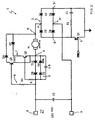
- FIG. 1 generally and schematically shown at 1 is a circuit device according to the invention for driving electric loads M which are supplied an A.C. current.
- These loads could be electric motors, or electric apparatus of any other types presenting a resistive/inductive load and to be driven by varying the mains supply voltage.
- the 220V A.C. mains supply is represented by a pair of plugs 4, 5 having a filtering capacitor C2 connected across them.
- the circuit device of this invention includes a bridge type of rectifying structure 2 which is connected between a mains plug 5 and the electric load M.
- the bridge 2 has two input terminals A, A' and two output terminals B, B'.
- the bridge 2 comprises diodes D1, D2, D3, D4.
- the input terminal A is connected to a terminating node H of the electric load M, and the other terminal A' is connected to the mains plug 5.
- the output B, B' of the bridge 2 is connected to an electronic switch 3 which is controlled by a signal PWM.
- a series of a resistor R1 and a capacitor C1 which are connected between the output terminals B, B' of the bridge 2.
- a discrete bipolar transistor Q1 of the NPN power type, receives the signal PWM on its base terminal, and has its conduction terminals connected between the output terminal B of the bridge 2 and a ground reference supply GND.
- the other output terminal B' is also taken to the ground reference GND.
- the device of this invention comprises a bi-directional current loop-back arrangement which is controlled by the same current as is flowed through the inductive windings of the electric load M.
- a double loop-back circuit path is provided, according to the invention, in parallel with the electric load M.
- a first component pair formed of a selection transistor Q2 and a diode D7 are arranged to form, in accordance with the invention, a first circuit path between the mains plug 4 and the nodes H, K at the input of the electric load M.
- a second pair formed of a selection transistor Q3 and a diode D9 are arranged, according to the invention, to form a second circuit path 8 between the mains plug 4 and the nodes H, K at the electric load M input.
- the first path 7 comprises the NPN bipolar transistor Q2, acting as a selector and having its base terminal connected to the mains plug 4 via a resistor R.
- the conduction, or collector and emitter, terminals of this transistor Q2 are connected to the node H of the load M, via a diode D7, and to the node K of the load M, respectively.
- the second circuit path 8 comprises a bipolar transistor Q3, acting as a selector and having its base terminal connected to the mains plug 4 via a resistor R2.
- This transistor Q3 is a PNP transistor.
- the conduction, or collector and emitter, terminals of the transistor Q3 are connected to the node K of the load M, and via a diode D9 to the node H of the load M, respectively.
- the selection of the two diodes D7 and D9 is differently provided using the positive and negative half-waves of the mains voltage signal.
- the structure of the device 1 also comprises a double pair 6 of diodes D1, D6, D8 and D10, which diodes are connected in antiparallel and essentially connected between the bases and the emitters of both transistors Q2 and Q3.
- This double diode pair 6 is further connected between the mains plug 4 and the terminating input node K of the load M.
- a capacitor C3 is connected between the input and the output of the double diode pair 6.
- first 7 and second 8 paths connected in parallel to the electric load are alternately activated, according to whether the positive half-wave or the negative half-wave happens to be present on the supply line.
- the transistor Q2 would be brought to its saturation range, and the transistor Q3 would be blocked.
- the capacitor C3 is effective to filter the voltage drop of this series of diodes D1, D6, preventing the transistors from being turned off when the power switch 3 is turned off.
- Figure 3 shows schematically a voltage vs. time plot of the base-emitter voltage drop through a full cycle of the mains supply, and the corresponding change in the loop-back current during one of the mains half-waves.
- Figure 4 Shown in Figure 4 is the pattern of the current through the transistor Q1, over a full cycle of the mains supply.
- Figure 4A which has the same time base as Figure 4, the reversal of the mains negative half-wave, as provided by the rectifying bridge 2 formed of the diodes D2, D3, D4 and D5, is shown.
- the series of the two diodes D1, D8 connected in antiparallel ensures saturation of the transistors even at low values of the current being flowed therethrough, and hence low operating power values of the load M.
- the series of the resistor R1 and the capacitor C1, in parallel with the power switch 3, allows the overvoltage peaks to be kept low, along with the voltage differential and the voltage fluctuations in the upper region of the mains sinusoid.
- the size of the components R2 and C2 will be selected at the designing stage to suit the type of the electric load and the type of the switch used.
- FIGS 5 and 5A illustrate schematically the patterns for the switch 3 current and voltage. As can be seen, the voltage peak has been well flattened in the upper region. This is made possible by the loop-back paths provided by the invention.
- Figure 5A shows, in particular, the mains sinusoid envelope.
- a major advantage of the circuit according to the invention is that the overvoltage problems of the power switch 3 have now been significantly attenuated by the use of devices which can operate on a lower voltage, besides being more cost-efficient.
- Figure 6 shows schematically a modified embodiment, denoted by the numeral 10, of the circuit device according to the invention.
- the second path 8 also includes an NPN transistor Q4.
- circuit portion which comprises the antiparallel diodes.
- two discrete portions 6', 6'' are provided, each comprising a single diode and a series of two diodes connected in antiparallel to the single diode, as shown in Figure 6.
- the voltage drop is positive with respect to the potential at the base of the transistor Q2.
- the voltage drop across the diode series D6, D8 is sufficient to bias the transistor Q2.
- the transistor Q2 is held blocked, and the transistor Q3 brought to the saturation range, enabling the diode D9 to loop back the current.
- the device of this invention can be readily adapted for driving three-phase electric loads, as shown schematically in Figure 7.
- the circuit device does solve the technical problem, and affords a number of advantages, foremost among which is that the electric load can be connected directly to the A.C. mains supply.
- the power regulation provided by this device is linear throughout the regulated range.
- the device of this invention can make the operation of electric motors effectively less noisy in many applications.
Landscapes
- Engineering & Computer Science (AREA)
- Power Engineering (AREA)
- Power Conversion In General (AREA)
- Inverter Devices (AREA)
Priority Applications (3)
| Application Number | Priority Date | Filing Date | Title |
|---|---|---|---|
| DE69814426T DE69814426D1 (de) | 1998-12-31 | 1998-12-31 | Schaltungvorrichtung zur Steuerung einer elektrischen Wechselstromlast |
| EP98830809A EP1017156B1 (fr) | 1998-12-31 | 1998-12-31 | Dispositif de circuit pour commander une charge électrique à courant alternatif |
| US09/476,489 US6256211B1 (en) | 1998-12-31 | 1999-12-30 | Circuit device for driving an a.c. electric load |
Applications Claiming Priority (1)
| Application Number | Priority Date | Filing Date | Title |
|---|---|---|---|
| EP98830809A EP1017156B1 (fr) | 1998-12-31 | 1998-12-31 | Dispositif de circuit pour commander une charge électrique à courant alternatif |
Publications (2)
| Publication Number | Publication Date |
|---|---|
| EP1017156A1 true EP1017156A1 (fr) | 2000-07-05 |
| EP1017156B1 EP1017156B1 (fr) | 2003-05-07 |
Family
ID=8236953
Family Applications (1)
| Application Number | Title | Priority Date | Filing Date |
|---|---|---|---|
| EP98830809A Expired - Lifetime EP1017156B1 (fr) | 1998-12-31 | 1998-12-31 | Dispositif de circuit pour commander une charge électrique à courant alternatif |
Country Status (3)
| Country | Link |
|---|---|
| US (1) | US6256211B1 (fr) |
| EP (1) | EP1017156B1 (fr) |
| DE (1) | DE69814426D1 (fr) |
Cited By (7)
| Publication number | Priority date | Publication date | Assignee | Title |
|---|---|---|---|---|
| WO2002078160A1 (fr) * | 2001-03-25 | 2002-10-03 | S.M.M. Pulse System Ltd. | Procede et systeme de commande d'un dispositif electromagnetique |
| EP1304792A1 (fr) * | 2001-10-19 | 2003-04-23 | STMicroelectronics S.r.l. | Dispositif de circuit pour commander une charge électrique à courant alternatif |
| GB2396441A (en) * | 2002-12-20 | 2004-06-23 | Motorola Inc | Circuit and method for supplying an electrical A. C. load |
| CN101783514A (zh) * | 2010-03-09 | 2010-07-21 | 李香龙 | 一种交流负载功率因数的校正方法及电路 |
| WO2008110964A3 (fr) * | 2007-03-09 | 2011-05-12 | Koninklijke Philips Electronics N.V. | Commander une puissance d'un moteur électrique |
| DE102010028506A1 (de) | 2010-05-03 | 2011-11-03 | BSH Bosch und Siemens Hausgeräte GmbH | Schaltung und Verfahren zur Ansteuerung eines Linearverdichters |
| CN111834308A (zh) * | 2019-04-16 | 2020-10-27 | G.卡梯埃技术公司 | 用于电动致动器的最佳冷却控制设备 |
Families Citing this family (4)
| Publication number | Priority date | Publication date | Assignee | Title |
|---|---|---|---|---|
| FR2845480A1 (fr) * | 2002-10-07 | 2004-04-09 | St Microelectronics Sa | Protection d'un interrupteur en alternatif |
| BRPI0613240A2 (pt) * | 2005-06-06 | 2012-12-04 | Lutron Electronics Co | aparelho e método e apararelho para controlar a velocidade de um motor variável silencioso |
| US7489094B2 (en) | 2005-11-18 | 2009-02-10 | Lutron Electronics Co., Inc. | Method and apparatus for quiet fan speed control |
| US11159160B2 (en) * | 2017-07-27 | 2021-10-26 | Toshiba Mitsubishi-Electric Industrial Systems Corporation | AC switch, and uninterruptible power supply and voltage sag compensator including AC switch |
Citations (2)
| Publication number | Priority date | Publication date | Assignee | Title |
|---|---|---|---|---|
| EP0221574A2 (fr) * | 1985-11-08 | 1987-05-13 | Asea Brown Boveri Aktiengesellschaft | Circuit pour régulateur à courant alternatif à commande par impulsion |
| EP0573197A1 (fr) * | 1992-06-04 | 1993-12-08 | Strand Lighting Limited | Système composés de gradateurs et gradateur destiné à un tel système |
Family Cites Families (2)
| Publication number | Priority date | Publication date | Assignee | Title |
|---|---|---|---|---|
| GB9408056D0 (en) * | 1994-04-22 | 1994-06-15 | Switched Reluctance Drives Ltd | A control circuit for an inductive load |
| DE19709264A1 (de) * | 1997-03-06 | 1998-09-10 | Hilti Ag | Verfahren zur Reduzierung von Rückwirkungen auf den Verlauf des einem Netz entnommenen Stroms bei induktiven Lasten und Vorrichtung zum Antreiben von Motoren nach diesem Verfahren |
-
1998
- 1998-12-31 EP EP98830809A patent/EP1017156B1/fr not_active Expired - Lifetime
- 1998-12-31 DE DE69814426T patent/DE69814426D1/de not_active Expired - Lifetime
-
1999
- 1999-12-30 US US09/476,489 patent/US6256211B1/en not_active Expired - Lifetime
Patent Citations (2)
| Publication number | Priority date | Publication date | Assignee | Title |
|---|---|---|---|---|
| EP0221574A2 (fr) * | 1985-11-08 | 1987-05-13 | Asea Brown Boveri Aktiengesellschaft | Circuit pour régulateur à courant alternatif à commande par impulsion |
| EP0573197A1 (fr) * | 1992-06-04 | 1993-12-08 | Strand Lighting Limited | Système composés de gradateurs et gradateur destiné à un tel système |
Cited By (14)
| Publication number | Priority date | Publication date | Assignee | Title |
|---|---|---|---|---|
| WO2002078160A1 (fr) * | 2001-03-25 | 2002-10-03 | S.M.M. Pulse System Ltd. | Procede et systeme de commande d'un dispositif electromagnetique |
| EP1304792A1 (fr) * | 2001-10-19 | 2003-04-23 | STMicroelectronics S.r.l. | Dispositif de circuit pour commander une charge électrique à courant alternatif |
| US6909258B2 (en) | 2001-10-19 | 2005-06-21 | Stmicroelectronics S.R.L. | Circuit device for driving an AC electric load |
| EP2317637A1 (fr) * | 2001-10-19 | 2011-05-04 | STMicroelectronics S.r.l. | Dispositif de circuit pour commander une charge électrique à courant alternatif |
| GB2396441A (en) * | 2002-12-20 | 2004-06-23 | Motorola Inc | Circuit and method for supplying an electrical A. C. load |
| GB2396441B (en) * | 2002-12-20 | 2005-11-30 | Motorola Inc | Circuit and method for supplying an electrical a.c. load |
| US7015679B2 (en) | 2002-12-20 | 2006-03-21 | Freescale Semiconductor, Inc. | Circuit and method for supplying an electrical a.c. load |
| US8125179B2 (en) | 2007-03-09 | 2012-02-28 | Koninklijke Philips Electronics N.V. | Controlling a power of an electrical motor |
| WO2008110964A3 (fr) * | 2007-03-09 | 2011-05-12 | Koninklijke Philips Electronics N.V. | Commander une puissance d'un moteur électrique |
| CN101783514A (zh) * | 2010-03-09 | 2010-07-21 | 李香龙 | 一种交流负载功率因数的校正方法及电路 |
| CN101783514B (zh) * | 2010-03-09 | 2013-04-03 | 河北工业大学 | 一种交流负载功率因数的校正方法及电路 |
| WO2011138110A1 (fr) | 2010-05-03 | 2011-11-10 | BSH Bosch und Siemens Hausgeräte GmbH | Circuit et procédé de commande d'un compresseur linéaire |
| DE102010028506A1 (de) | 2010-05-03 | 2011-11-03 | BSH Bosch und Siemens Hausgeräte GmbH | Schaltung und Verfahren zur Ansteuerung eines Linearverdichters |
| CN111834308A (zh) * | 2019-04-16 | 2020-10-27 | G.卡梯埃技术公司 | 用于电动致动器的最佳冷却控制设备 |
Also Published As
| Publication number | Publication date |
|---|---|
| EP1017156B1 (fr) | 2003-05-07 |
| US6256211B1 (en) | 2001-07-03 |
| DE69814426D1 (de) | 2003-06-12 |
Similar Documents
| Publication | Publication Date | Title |
|---|---|---|
| EP1952527B1 (fr) | Procede et appareil de commande de la vitesse d'un ventilateur silencieux | |
| EP1017156B1 (fr) | Dispositif de circuit pour commander une charge électrique à courant alternatif | |
| JP5753275B2 (ja) | 電力変換装置の駆動装置および電力変換装置の駆動方法 | |
| US5789894A (en) | Solid state motor speed control | |
| US6294901B1 (en) | Power dimmer | |
| US7015679B2 (en) | Circuit and method for supplying an electrical a.c. load | |
| GB2071939A (en) | Drive circuit arrangements of brushless dc motors | |
| US20070194745A1 (en) | Split phase polyphase inverter | |
| EP0666703A1 (fr) | Circuit de commande pour transistor de puissance pour appareil de chauffage par induction | |
| EP2317637B1 (fr) | Dispositif de circuit pour commander une charge électrique à courant alternatif | |
| US4242624A (en) | Direct current stepper motor with a permanent magnet rotor and electronic commutation device | |
| US6266258B1 (en) | Power substrate element topology | |
| EP0444404B1 (fr) | Interface de pont à haute tension pour régulation de moteur à courant alternatif et à courant continu sans balai | |
| JP6254116B2 (ja) | 電力変換装置の駆動装置および電力変換装置の駆動方法 | |
| JP2958075B2 (ja) | 交流電圧制御装置 | |
| CN222484953U (zh) | 一种电磁加热软启动电路以及电磁加热设备 | |
| CN1169214A (zh) | 串激电机的速度控制装置 | |
| US6831441B1 (en) | Speed regulator by pulse width modulation for direct current motors | |
| KR100317382B1 (ko) | 에스알엠모터의전원공급및구동회로 | |
| JP3246354B2 (ja) | 電動機駆動装置 | |
| JP4483006B2 (ja) | インバータ装置 | |
| JP2001178183A (ja) | インバータ装置 | |
| JPH07303388A (ja) | 信号発生回路 | |
| JPH09245952A (ja) | 高周波インバータ | |
| JPS62202213A (ja) | 交流負荷制御方式 |
Legal Events
| Date | Code | Title | Description |
|---|---|---|---|
| PUAI | Public reference made under article 153(3) epc to a published international application that has entered the european phase |
Free format text: ORIGINAL CODE: 0009012 |
|
| AK | Designated contracting states |
Kind code of ref document: A1 Designated state(s): AT BE CH CY DE DK ES FI FR GB GR IE IT LI LU MC NL PT SE |
|
| AX | Request for extension of the european patent |
Free format text: AL;LT;LV;MK;RO;SI |
|
| 17P | Request for examination filed |
Effective date: 20001214 |
|
| AKX | Designation fees paid |
Free format text: DE FR GB IT |
|
| 17Q | First examination report despatched |
Effective date: 20011030 |
|
| GRAH | Despatch of communication of intention to grant a patent |
Free format text: ORIGINAL CODE: EPIDOS IGRA |
|
| GRAH | Despatch of communication of intention to grant a patent |
Free format text: ORIGINAL CODE: EPIDOS IGRA |
|
| GRAA | (expected) grant |
Free format text: ORIGINAL CODE: 0009210 |
|
| AK | Designated contracting states |
Designated state(s): DE FR GB IT |
|
| PG25 | Lapsed in a contracting state [announced via postgrant information from national office to epo] |
Ref country code: FR Free format text: LAPSE BECAUSE OF FAILURE TO SUBMIT A TRANSLATION OF THE DESCRIPTION OR TO PAY THE FEE WITHIN THE PRESCRIBED TIME-LIMIT Effective date: 20030507 |
|
| REG | Reference to a national code |
Ref country code: GB Ref legal event code: FG4D |
|
| REF | Corresponds to: |
Ref document number: 69814426 Country of ref document: DE Date of ref document: 20030612 Kind code of ref document: P |
|
| PG25 | Lapsed in a contracting state [announced via postgrant information from national office to epo] |
Ref country code: DE Free format text: LAPSE BECAUSE OF FAILURE TO SUBMIT A TRANSLATION OF THE DESCRIPTION OR TO PAY THE FEE WITHIN THE PRESCRIBED TIME-LIMIT Effective date: 20030808 |
|
| PLBE | No opposition filed within time limit |
Free format text: ORIGINAL CODE: 0009261 |
|
| STAA | Information on the status of an ep patent application or granted ep patent |
Free format text: STATUS: NO OPPOSITION FILED WITHIN TIME LIMIT |
|
| 26N | No opposition filed |
Effective date: 20040210 |
|
| EN | Fr: translation not filed | ||
| PGFP | Annual fee paid to national office [announced via postgrant information from national office to epo] |
Ref country code: GB Payment date: 20061127 Year of fee payment: 9 |
|
| PGFP | Annual fee paid to national office [announced via postgrant information from national office to epo] |
Ref country code: IT Payment date: 20061231 Year of fee payment: 9 |
|
| GBPC | Gb: european patent ceased through non-payment of renewal fee |
Effective date: 20071231 |
|
| PG25 | Lapsed in a contracting state [announced via postgrant information from national office to epo] |
Ref country code: GB Free format text: LAPSE BECAUSE OF NON-PAYMENT OF DUE FEES Effective date: 20071231 |
|
| PG25 | Lapsed in a contracting state [announced via postgrant information from national office to epo] |
Ref country code: IT Free format text: LAPSE BECAUSE OF NON-PAYMENT OF DUE FEES Effective date: 20071231 |