EP1017164A2 - Stromspiegel mit einem konstanten Strom über einen weiten Bereich der Ausgangslastimpedanz - Google Patents
Stromspiegel mit einem konstanten Strom über einen weiten Bereich der Ausgangslastimpedanz Download PDFInfo
- Publication number
- EP1017164A2 EP1017164A2 EP19990125651 EP99125651A EP1017164A2 EP 1017164 A2 EP1017164 A2 EP 1017164A2 EP 19990125651 EP19990125651 EP 19990125651 EP 99125651 A EP99125651 A EP 99125651A EP 1017164 A2 EP1017164 A2 EP 1017164A2
- Authority
- EP
- European Patent Office
- Prior art keywords
- transistor
- current
- current mirror
- output
- drain
- Prior art date
- Legal status (The legal status is an assumption and is not a legal conclusion. Google has not performed a legal analysis and makes no representation as to the accuracy of the status listed.)
- Withdrawn
Links
- 230000005669 field effect Effects 0.000 claims description 13
- 229910044991 metal oxide Inorganic materials 0.000 claims description 13
- 150000004706 metal oxides Chemical class 0.000 claims description 13
- XUIMIQQOPSSXEZ-UHFFFAOYSA-N Silicon Chemical compound [Si] XUIMIQQOPSSXEZ-UHFFFAOYSA-N 0.000 claims 12
- 229910052710 silicon Inorganic materials 0.000 claims 12
- 239000010703 silicon Substances 0.000 claims 12
- 239000008186 active pharmaceutical agent Substances 0.000 description 4
Images

Classifications
-
- H—ELECTRICITY
- H03—ELECTRONIC CIRCUITRY
- H03F—AMPLIFIERS
- H03F3/00—Amplifiers with only discharge tubes or only semiconductor devices as amplifying elements
- H03F3/34—DC amplifiers in which all stages are DC-coupled
- H03F3/343—DC amplifiers in which all stages are DC-coupled with semiconductor devices only
- H03F3/345—DC amplifiers in which all stages are DC-coupled with semiconductor devices only with field-effect devices
Definitions
- This application is related to a current mirror and more particularly to a current mirror capable of accepting a wide range of output load impedance while providing a substantially constant output current either identical or proportional to the input current.
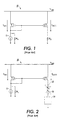
- the current mirror 10 comprises two p-channel metal oxide field effect transistors (PMOS) T 1 and T 2 .
- the sources of both transistors T 1 and T 2 are connected to a power supply V DD and the gates of both transistors T 1 and T 2 are connected each other.
- the gate and the drain of transistor T 1 are connected to each other.
- the drain of transistor T 1 is grounded through an impedance R 1 which represents the impedance of input current source 11 and the drain of transistor T 2 is grounded through an impedance R 2 which represents the output load impedance.
- Current source 11 supplies an input current I IN1 which flows through transistor T 1 .
- the gate of transistor T 1 is connected to its drain.
- a current mirror is designed to duplicate the input current I IN (the current through the transistor T 1 ) at the output as the output current I OUT (the current through transistor T 2 ) or to provide an output current I OUT proportional to the input current I IN1 by a set factor.
- the transistors have to be selected to be identical to generate identical currents or must have a size ratio equal to the set factor. Since the sizes of the transistors, the amount of currents and voltages can be adjusted to provide proportional currents, for the purpose of simplicity, hereinafter, the discussion will include only the current mirrors that provide identical currents.
- FIG. 2 there is shown a representation of output impedance and load impedance.
- the internal impedance of the current mirror which can be observed through the output node 12 at the drain of transistor T 2, is called output impedance R O .
- the internal impedance of the load 14 which can be observed from node 16 (the node that will be connected to node 12), is called load impedance R L .
- a current mirror should act as a current source to provide a constant current for any load impedance.
- the ideal current source model suggests an output impedance of infinity. If the output impedance is infinity, then regardless of the load impedance, the current source provides a constant current. However, since in reality the output impedance is not infinity, depending on the value of the load impedance, the current of the current mirror changes.
- a current mirror which utilizes two MOSFET transistors and an operational amplifier.
- the sources of both transistors are connected to a power supply and the gates of both transistors are connected to the output of the operational amplifier.
- the drain of one transistor is connected to one of the inputs of the operational amplifier and to a current source.
- the drain of the other transistor is connected to the other input of the operational amplifier and to a load impedance.
- Current mirror 20 comprises two same size PMOS transistors T 3 and T 4 .
- the sources of both transistors are connected to V DD , the drain of transistor T 3 is grounded through an impedance R 3 which represents the impedance of input current source 22, and the drain of transistor T 4 is grounded through a load impedance R 4 .
- the value of the load impedance R 4 is considered unknown.
- the positive input of an Op-Amp 24 is connected to the drain of transistor T 3 and the negative input of the Op-Amp 22 is connected to the drain of transistor T 4 .
- the output of the Op-Amp 24 is connected to the gate of transistor T 3 .
- the gate of transistor T 4 is connected to a biasing voltage V BIAS .
- the Op-Amp 24 works in a negative feedback mode and therefore forces the two voltages at its two inputs to be substantially equal. Since nodes 26 and 28 are connected to the positive and negative inputs of Op-Amp 22, they will have substantially the same voltage. With this configuration, node 28 will have the same voltage as the voltage of node 26 regardless of the value of the load impedance. Also, with this configuration, the output of the Op-amp 24 determines the proper voltage for the gate of the transistor T 3 to force the two voltages of nodes 26 and 28 to be equal.
- the Op-Amp 24 regulates the V GS of both transistors T 3 and T 4 to compensate for the changes of the V DS of transistor T 4 based on different load impedance. Therefore, in Figure 4, the V GS of both transistors become the controlling voltage for the current mirror 20.
- the disclosed embodiment of this invention provides a substantially constant_output current I OUT over a wide range of load impedance.
- Current mirror 20 utilizes two p-channel transistors. However, if one desires, the current mirror can be designed to use two n-channel transistors.
- the disclosed embodiments of this invention can be designed to scale the output current.
- the output current can be set to a desired value.
- the ratio of the size of the output transistor to the size of the input transistor determines the ratio between the input and output currents. If the size of the output transistor is larger or smaller than the size of the input transistor then, the output current will be larger or smaller respectively.
Landscapes
- Engineering & Computer Science (AREA)
- Power Engineering (AREA)
- Control Of Electrical Variables (AREA)
- Amplifiers (AREA)
Applications Claiming Priority (2)
| Application Number | Priority Date | Filing Date | Title |
|---|---|---|---|
| US22242898A | 1998-12-28 | 1998-12-28 | |
| US222428 | 1998-12-28 |
Publications (1)
| Publication Number | Publication Date |
|---|---|
| EP1017164A2 true EP1017164A2 (de) | 2000-07-05 |
Family
ID=22832168
Family Applications (1)
| Application Number | Title | Priority Date | Filing Date |
|---|---|---|---|
| EP19990125651 Withdrawn EP1017164A2 (de) | 1998-12-28 | 1999-12-22 | Stromspiegel mit einem konstanten Strom über einen weiten Bereich der Ausgangslastimpedanz |
Country Status (2)
| Country | Link |
|---|---|
| EP (1) | EP1017164A2 (de) |
| JP (1) | JP2000201032A (de) |
Cited By (2)
| Publication number | Priority date | Publication date | Assignee | Title |
|---|---|---|---|---|
| US8575999B2 (en) | 2009-07-07 | 2013-11-05 | Fujitsu Limited | Constant current circuit and semiconductor integrated circuit |
| US8659348B2 (en) | 2012-07-26 | 2014-02-25 | Hewlett-Packard Development Company, L.P. | Current mirrors |
Families Citing this family (4)
| Publication number | Priority date | Publication date | Assignee | Title |
|---|---|---|---|---|
| JP2006338434A (ja) * | 2005-06-03 | 2006-12-14 | New Japan Radio Co Ltd | 基準電圧発生回路 |
| JP4837111B2 (ja) * | 2009-03-02 | 2011-12-14 | 株式会社半導体理工学研究センター | 基準電流源回路 |
| EP2597931B1 (de) * | 2011-09-01 | 2015-05-27 | Silicon Touch Technology, Inc. | Treiberschaltung und zugehörige Fehlererkennungsschaltung und Verfahren hierfür |
| CN103186161B (zh) * | 2011-12-28 | 2015-10-28 | 国民技术股份有限公司 | 一种电流镜像电路 |
-
1999
- 1999-12-21 JP JP11362322A patent/JP2000201032A/ja not_active Withdrawn
- 1999-12-22 EP EP19990125651 patent/EP1017164A2/de not_active Withdrawn
Cited By (2)
| Publication number | Priority date | Publication date | Assignee | Title |
|---|---|---|---|---|
| US8575999B2 (en) | 2009-07-07 | 2013-11-05 | Fujitsu Limited | Constant current circuit and semiconductor integrated circuit |
| US8659348B2 (en) | 2012-07-26 | 2014-02-25 | Hewlett-Packard Development Company, L.P. | Current mirrors |
Also Published As
| Publication number | Publication date |
|---|---|
| JP2000201032A (ja) | 2000-07-18 |
Similar Documents
| Publication | Publication Date | Title |
|---|---|---|
| US5999052A (en) | High speed, fine-resolution gain programmable amplifier | |
| US6194967B1 (en) | Current mirror circuit | |
| US5959446A (en) | High swing current efficient CMOS cascode current mirror | |
| KR100275177B1 (ko) | 저전압차동증폭기 | |
| EP0880735B1 (de) | Cmos-stromspiegel | |
| CN109213248A (zh) | 负电源控制电路以及电源装置 | |
| KR920010237B1 (ko) | 증폭회로 | |
| US6344769B1 (en) | Precision differential switched current source | |
| JP2004194124A (ja) | ヒステリシスコンパレータ回路 | |
| US5043652A (en) | Differential voltage to differential current conversion circuit having linear output | |
| US6717451B1 (en) | Precision analog level shifter with programmable options | |
| US7187223B2 (en) | Comparator with hysteresis | |
| US8723593B2 (en) | Bias voltage generation circuit and differential circuit | |
| EP1017164A2 (de) | Stromspiegel mit einem konstanten Strom über einen weiten Bereich der Ausgangslastimpedanz | |
| US6181195B1 (en) | Impedance transport circuit | |
| JPH0758557A (ja) | 演算増幅器、演算増幅器のdcバイアス回路および演算増幅器をバイアスする方法 | |
| JPH11272786A (ja) | 差動増幅回路 | |
| JP2000286653A (ja) | 相互コンダクタンス増幅器及びこれを用いた自動利得制御装置 | |
| US6583665B2 (en) | Differential amplifier having active load device scaling | |
| EP0711032A1 (de) | Eingangsstufe für CMOS-Operationsverstärker und Verfahren dazu | |
| JP2550871B2 (ja) | Cmos定電流源回路 | |
| US6903607B2 (en) | Operational amplifier | |
| US6118341A (en) | Device with common mode feedback for a differential output | |
| JP4811157B2 (ja) | 増幅器 | |
| US5719524A (en) | Circuit having an input terminal for controlling two functions |
Legal Events
| Date | Code | Title | Description |
|---|---|---|---|
| PUAI | Public reference made under article 153(3) epc to a published international application that has entered the european phase |
Free format text: ORIGINAL CODE: 0009012 |
|
| AK | Designated contracting states |
Kind code of ref document: A2 Designated state(s): AT BE CH CY DE DK ES FI FR GB GR IE IT LI LU MC NL PT SE |
|
| AX | Request for extension of the european patent |
Free format text: AL;LT;LV;MK;RO;SI |
|
| STAA | Information on the status of an ep patent application or granted ep patent |
Free format text: STATUS: THE APPLICATION IS DEEMED TO BE WITHDRAWN |
|
| 18D | Application deemed to be withdrawn |
Effective date: 20020701 |