EP1017645B1 - Procede de realisation d'un panneau de visualisation comportant une dalle a stabilite dimensionnelle amelioree - Google Patents
Procede de realisation d'un panneau de visualisation comportant une dalle a stabilite dimensionnelle amelioree Download PDFInfo
- Publication number
- EP1017645B1 EP1017645B1 EP98945357A EP98945357A EP1017645B1 EP 1017645 B1 EP1017645 B1 EP 1017645B1 EP 98945357 A EP98945357 A EP 98945357A EP 98945357 A EP98945357 A EP 98945357A EP 1017645 B1 EP1017645 B1 EP 1017645B1
- Authority
- EP
- European Patent Office
- Prior art keywords
- glass
- bath
- slab
- display panel
- process according
- Prior art date
- Legal status (The legal status is an assumption and is not a legal conclusion. Google has not performed a legal analysis and makes no representation as to the accuracy of the status listed.)
- Expired - Lifetime
Links
- 238000004519 manufacturing process Methods 0.000 title claims description 7
- 239000011521 glass Substances 0.000 claims description 21
- 238000000034 method Methods 0.000 claims description 13
- 238000010438 heat treatment Methods 0.000 claims description 11
- 125000006850 spacer group Chemical group 0.000 claims description 9
- 230000004888 barrier function Effects 0.000 claims description 7
- 150000003839 salts Chemical class 0.000 claims description 6
- 229910052751 metal Inorganic materials 0.000 claims description 3
- 239000002184 metal Substances 0.000 claims description 3
- 238000007654 immersion Methods 0.000 claims 2
- 229910003002 lithium salt Inorganic materials 0.000 claims 1
- 159000000002 lithium salts Chemical class 0.000 claims 1
- XAEFZNCEHLXOMS-UHFFFAOYSA-M potassium benzoate Chemical compound [K+].[O-]C(=O)C1=CC=CC=C1 XAEFZNCEHLXOMS-UHFFFAOYSA-M 0.000 claims 1
- 159000000000 sodium salts Chemical class 0.000 claims 1
- 238000002791 soaking Methods 0.000 description 8
- 239000005361 soda-lime glass Substances 0.000 description 7
- CPLXHLVBOLITMK-UHFFFAOYSA-N Magnesium oxide Chemical compound [Mg]=O CPLXHLVBOLITMK-UHFFFAOYSA-N 0.000 description 6
- OAICVXFJPJFONN-UHFFFAOYSA-N Phosphorus Chemical compound [P] OAICVXFJPJFONN-UHFFFAOYSA-N 0.000 description 6
- 238000000151 deposition Methods 0.000 description 6
- 238000010411 cooking Methods 0.000 description 5
- 230000008021 deposition Effects 0.000 description 5
- 239000000463 material Substances 0.000 description 5
- 238000011282 treatment Methods 0.000 description 4
- 238000005056 compaction Methods 0.000 description 3
- 238000001816 cooling Methods 0.000 description 3
- 239000003989 dielectric material Substances 0.000 description 3
- 239000000395 magnesium oxide Substances 0.000 description 3
- 238000010791 quenching Methods 0.000 description 3
- 230000000171 quenching effect Effects 0.000 description 3
- 229910001415 sodium ion Inorganic materials 0.000 description 3
- 239000000126 substance Substances 0.000 description 3
- DGAQECJNVWCQMB-PUAWFVPOSA-M Ilexoside XXIX Chemical compound C[C@@H]1CC[C@@]2(CC[C@@]3(C(=CC[C@H]4[C@]3(CC[C@@H]5[C@@]4(CC[C@@H](C5(C)C)OS(=O)(=O)[O-])C)C)[C@@H]2[C@]1(C)O)C)C(=O)O[C@H]6[C@@H]([C@H]([C@@H]([C@H](O6)CO)O)O)O.[Na+] DGAQECJNVWCQMB-PUAWFVPOSA-M 0.000 description 2
- ZLMJMSJWJFRBEC-UHFFFAOYSA-N Potassium Chemical compound [K] ZLMJMSJWJFRBEC-UHFFFAOYSA-N 0.000 description 2
- VYPSYNLAJGMNEJ-UHFFFAOYSA-N Silicium dioxide Chemical compound O=[Si]=O VYPSYNLAJGMNEJ-UHFFFAOYSA-N 0.000 description 2
- 229910052783 alkali metal Inorganic materials 0.000 description 2
- 150000001340 alkali metals Chemical class 0.000 description 2
- 238000003491 array Methods 0.000 description 2
- 230000006835 compression Effects 0.000 description 2
- 238000007906 compression Methods 0.000 description 2
- 150000002500 ions Chemical class 0.000 description 2
- 239000000203 mixture Substances 0.000 description 2
- 229910052700 potassium Inorganic materials 0.000 description 2
- 239000011591 potassium Substances 0.000 description 2
- 229910052708 sodium Inorganic materials 0.000 description 2
- 239000011734 sodium Substances 0.000 description 2
- 238000012800 visualization Methods 0.000 description 2
- WHXSMMKQMYFTQS-UHFFFAOYSA-N Lithium Chemical compound [Li] WHXSMMKQMYFTQS-UHFFFAOYSA-N 0.000 description 1
- 229910002651 NO3 Inorganic materials 0.000 description 1
- NHNBFGGVMKEFGY-UHFFFAOYSA-N Nitrate Chemical compound [O-][N+]([O-])=O NHNBFGGVMKEFGY-UHFFFAOYSA-N 0.000 description 1
- BQCADISMDOOEFD-UHFFFAOYSA-N Silver Chemical compound [Ag] BQCADISMDOOEFD-UHFFFAOYSA-N 0.000 description 1
- 229910052810 boron oxide Inorganic materials 0.000 description 1
- 239000003086 colorant Substances 0.000 description 1
- 210000003298 dental enamel Anatomy 0.000 description 1
- JKWMSGQKBLHBQQ-UHFFFAOYSA-N diboron trioxide Chemical compound O=BOB=O JKWMSGQKBLHBQQ-UHFFFAOYSA-N 0.000 description 1
- 239000006185 dispersion Substances 0.000 description 1
- 238000010304 firing Methods 0.000 description 1
- 230000009477 glass transition Effects 0.000 description 1
- 238000005342 ion exchange Methods 0.000 description 1
- HTUMBQDCCIXGCV-UHFFFAOYSA-N lead oxide Chemical compound [O-2].[Pb+2] HTUMBQDCCIXGCV-UHFFFAOYSA-N 0.000 description 1
- 229910000464 lead oxide Inorganic materials 0.000 description 1
- 229910052744 lithium Inorganic materials 0.000 description 1
- 238000012423 maintenance Methods 0.000 description 1
- 230000000873 masking effect Effects 0.000 description 1
- 229910001414 potassium ion Inorganic materials 0.000 description 1
- 159000000001 potassium salts Chemical class 0.000 description 1
- 230000005855 radiation Effects 0.000 description 1
- 230000035939 shock Effects 0.000 description 1
- 239000000377 silicon dioxide Substances 0.000 description 1
- 229910052709 silver Inorganic materials 0.000 description 1
- 239000004332 silver Substances 0.000 description 1
- HUAUNKAZQWMVFY-UHFFFAOYSA-M sodium;oxocalcium;hydroxide Chemical compound [OH-].[Na+].[Ca]=O HUAUNKAZQWMVFY-UHFFFAOYSA-M 0.000 description 1
- 230000000087 stabilizing effect Effects 0.000 description 1
- 238000003860 storage Methods 0.000 description 1
- 230000007704 transition Effects 0.000 description 1
Images
Classifications
-
- H—ELECTRICITY
- H01—ELECTRIC ELEMENTS
- H01J—ELECTRIC DISCHARGE TUBES OR DISCHARGE LAMPS
- H01J9/00—Apparatus or processes specially adapted for the manufacture, installation, removal, maintenance of electric discharge tubes, discharge lamps, or parts thereof; Recovery of material from discharge tubes or lamps
- H01J9/20—Manufacture of screens on or from which an image or pattern is formed, picked up, converted or stored; Applying coatings to the vessel
-
- C—CHEMISTRY; METALLURGY
- C03—GLASS; MINERAL OR SLAG WOOL
- C03B—MANUFACTURE, SHAPING, OR SUPPLEMENTARY PROCESSES
- C03B27/00—Tempering or quenching glass products
- C03B27/02—Tempering or quenching glass products using liquid
- C03B27/03—Tempering or quenching glass products using liquid the liquid being a molten metal or a molten salt
-
- H—ELECTRICITY
- H01—ELECTRIC ELEMENTS
- H01J—ELECTRIC DISCHARGE TUBES OR DISCHARGE LAMPS
- H01J2217/00—Gas-filled discharge tubes
- H01J2217/38—Cold-cathode tubes
- H01J2217/49—Display panels, e.g. not making use of alternating current
- H01J2217/492—Details
- H01J2217/49264—Vessels
Definitions
- the present invention relates to display panels image whose slabs must maintain dimensions substantially constant throughout their manufacturing process. It concerns more particularly a method of producing a display panel image which is particularly suitable for these applications.
- This process applies in particular to plasma panels of all types, alternative to coplanar maintenance (ACC), alternative type XY, to direct current, and to field emission panels (FED) which undergo heat treatments during their manufacture.
- ACC coplanar maintenance
- XY direct current
- FED field emission panels
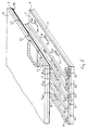
- a plasma display panel uses two glass tiles on which are deposited one or more networks of electrodes. Slabs are joined together so that the electrode arrays are substantially orthogonal. Each intersection of electrodes defines a cell to which a gas space corresponds.
- first slab 2 which forms the front face of the panel visualization, i.e. the face that an observer is looking at, are deposited one or more arrays of metal electrodes Y1 to Y3.
- metal electrodes Y1 to Y3 There is only one network for type X, Y panels and two for type panels coplanar which also applies the method according to the invention. This deposit can be done under vacuum.
- the electrodes Y1 to Y3 are then covered with a layer 5 of dielectric material including on the surface a layer of magnesia 50.
- the electrodes X1 to X5 are also covered with a layer 6 of dielectric material generally also including, on the surface, a layer of magnesia (not shown).
- the dielectric layer 6 is covered with layers forming bands 7, 8, 9 of phosphor materials corresponding for example to the colors green, red and blue.
- the phosphor strips 7, 8, 9 are arranged in parallel to electrodes X1 to X5.
- Y phosphor strips 7, 8, 9 are equipped with Ep1, Ep2, ... Epm savings level of the facing surfaces of two crossed electrodes X1 to X5 and Y1 to Y3.
- Each savings Ep1, Ep2 ... Epn materializes a cell C1, C2 ..., Cn.
- the phosphor strips 7, 8, 9 are separated by barriers 11 which have a confinement function. They prevent the spread from a discharge to neighboring unaddressed cells.
- spacers 12 are used so that the distance between the two slabs 2, 3 or the height of the gas space is substantially constant.
- spacers 12 are produced on one of the two slabs and during the assembly, the other slab abuts against them.
- the quality of panel operation may be degraded if the height of the space gas shows too large variations.
- the dielectric layers 5, 6 are produced, for example, by an enamel based on lead oxide, silica and boron oxide. This deposit is made hot at temperatures of about 580 ° C, which is higher than the softening temperature of ordinary soda lime glass used for slabs 2, 3.
- barriers 11 which can also play a role spacers, is done by layering and baking at temperatures between about 480 ° C and 550 ° C.
- the deposit of the phosphors 7, 8, 9 includes a firing phase at temperatures between 400 ° C and 480 ° C.
- the performance of the panel depends on the geometric and dimensional characteristics of cells and therefore of quality of registration, that is to say the precision of the positioning of these elements relative to each other.
- the electrodes Y1 to Y5 must be correctly positioned on the slab before 2 then after the deposition of the layer of dielectric material 5 and magnesia 50, the spacers 12 must be correctly positioned.
- the main difficulty in making such registrations comes from dimensional variations of slabs 2, 3 when subjected to a heat treatment.
- the glass tiles commonly used are glass soda-lime with a glass transition temperature Tg of the order of 520 ° C.
- Tg glass transition temperature
- This type of glass displays large variations in dimensions in one way or the other (compaction or expansion) when returning to room temperature after heat treatment. These variations are a compaction of the order of 400 to 600 ppm when cooking at approximately 600 ° C. These variations are difficult to take into account in view of the registration because they are not reproducible better than several tens of ppm.
- This cooking step barely meets the requirements of tolerance mentioned above and is expensive and difficult to achieve because the glass with tendency to warp and lose its flatness.
- the present invention aims to remedy these problems of dimensional variations by proposing a method for producing a image display panel comprising at least one glass slab especially soda-lime glass.
- Such a slab has the great advantage of a low material cost and more present, greater resistance to shocks and stresses thermal.
- the realization of the slab includes a soaking operation of the glass in a bath containing at least one molten salt of an alkali metal, a temperature above about 450 ° C, for more than an hour.
- the slab is then subjected to at least one heat treatment during a deposition operation of at least one element such as electrode, layer dielectric, spacer, barrier. Soaking in the bath aims to stabilize the dimensions of the slab during heat treatment.
- the molten salt can advantageously be a salt (for example a nitrate) of sodium and / or potassium and / or lithium.
- the soaking time is about 8 hours.
- the method of producing a panel of image display comprising at least one glass slab comprises a glass soaking operation in a bath containing at least one salt molten from an alkali metal, at a temperature above about 450 ° C, for more than an hour.
- At least one phenomenon occurs during this soaking. he it is a dimensional variation of the glass. However, during subsequent heat treatments to which the slab will be subjected, during deposition of elements such as electrodes, dielectric layers, barriers, spacers, its dimensional variations will be quite acceptable and may be taken into account for registration. The use of such a slab makes it possible to control better than 30 ppm its dimensions throughout the panel manufacturing cycle.
- the parameters of the chemical quenching treatment namely the composition of the bath, its temperature and the duration of soaking can be adapted according to the subsequent heat treatments inflicted on the slab and in particular of the following parameters temperature, cooking time and cooling rate.
- a slab 3 millimeters thick undergoing a soaking for 8 hours in a bath containing potassium salts to 460 ° C will have a zero mean compaction value with.
- the dimension of potassium ions being larger than that of sodium ions, the stresses in the surface glass and up to a few microns deep, are modified and in particular the surface of the glass is in compression after chemical quenching.
- the first baking at high temperature for example for depositing layers dielectric or possibly electrodes, if they are made in silver paste, potassium which was on the diffuse surface in the glass, surface stresses relax and the surface is no longer in compression.
- Such a slab, after its chemical quenching treatment is much more impact resistant and better withstands temperature than a soda lime glass slab conventionally used. This advantage is appreciable during transport and storage of slabs before undertaking heat treatment.
- the present invention applies to all types of visualization whose manufacturing cycle has heat treatments at temperatures above about 400 ° C.
Landscapes
- Chemical & Material Sciences (AREA)
- Engineering & Computer Science (AREA)
- Physics & Mathematics (AREA)
- Thermal Sciences (AREA)
- Materials Engineering (AREA)
- Organic Chemistry (AREA)
- Manufacturing & Machinery (AREA)
- Gas-Filled Discharge Tubes (AREA)
- Glass Compositions (AREA)
- Surface Treatment Of Glass (AREA)
- Manufacture Of Electron Tubes, Discharge Lamp Vessels, Lead-In Wires, And The Like (AREA)
Description
Claims (6)
- Procédé de réalisation d'un panneau de visualisation comportant au moins une dalle en verre, dont les dimensions sont conservées sensiblement constantes lorsqu'elle est soumise à au moins un traitement thermique lors d'une opération de dépôt sur la dalle d'au moins un élément tel qu'électrode, couche diélectrique, espaceur, barrière, caractérisé en ce qu'il comporte avant le traitement thermique, pour stabiliser les dimensions de la dalle, une opération de trempage du verre de la dalle dans un bain contenant au moins un sel fondu d'un métal alcalin, à une température supérieure à environ 450°C, pendant plus d'une heure.
- Procédé selon la revendication 1, caractérisé en ce que la durée du trempage est d'environ huit heures.
- Procédé selon l'une des revendications 1 à 2, caractérisé en ce que la température du bain est d'environ 460°C.
- Procédé selon l'une des revendications 1 à 3, caractérisé en ce que le bain contient au moins un sel de potassium.
- Procédé selon l'une des revendications 1 à 4, caractérisé en ce que le bain contient au moins un sel de sodium.
- Procédé selon l'une des revendications 1 à 5, caractérisé en ce que le bain contient au moins un sel de lithium.
Applications Claiming Priority (3)
| Application Number | Priority Date | Filing Date | Title |
|---|---|---|---|
| FR9711815A FR2768857B1 (fr) | 1997-09-23 | 1997-09-23 | Procede de realisation d'un panneau de visualisation comportant une dalle a stabilite dimensionnelle amelioree |
| FR9711815 | 1997-09-23 | ||
| PCT/FR1998/002033 WO1999015472A1 (fr) | 1997-09-23 | 1998-09-22 | Procede de realisation d'un panneau de visualisation comportant une dalle a stabilite dimensionnelle amelioree |
Publications (2)
| Publication Number | Publication Date |
|---|---|
| EP1017645A1 EP1017645A1 (fr) | 2000-07-12 |
| EP1017645B1 true EP1017645B1 (fr) | 2002-01-23 |
Family
ID=9511367
Family Applications (1)
| Application Number | Title | Priority Date | Filing Date |
|---|---|---|---|
| EP98945357A Expired - Lifetime EP1017645B1 (fr) | 1997-09-23 | 1998-09-22 | Procede de realisation d'un panneau de visualisation comportant une dalle a stabilite dimensionnelle amelioree |
Country Status (7)
| Country | Link |
|---|---|
| EP (1) | EP1017645B1 (fr) |
| JP (1) | JP2001517854A (fr) |
| KR (1) | KR20010023586A (fr) |
| CN (1) | CN1272098A (fr) |
| DE (1) | DE69803590T2 (fr) |
| FR (1) | FR2768857B1 (fr) |
| WO (1) | WO1999015472A1 (fr) |
Families Citing this family (1)
| Publication number | Priority date | Publication date | Assignee | Title |
|---|---|---|---|---|
| US11453612B2 (en) | 2016-04-20 | 2022-09-27 | Corning Incorporated | Glass-based articles including a metal oxide concentration gradient |
Family Cites Families (8)
| Publication number | Priority date | Publication date | Assignee | Title |
|---|---|---|---|---|
| JPS62209414A (ja) * | 1986-03-10 | 1987-09-14 | Alps Electric Co Ltd | 液晶表示素子 |
| JPH0818850B2 (ja) * | 1986-09-05 | 1996-02-28 | セントラル硝子株式会社 | 化学強化ガラス |
| US5296294A (en) * | 1987-02-03 | 1994-03-22 | Nippon Sheet Glass Co., Ltd. | Glass panel resistant to coloring when irradiated with electron rays |
| US4897371A (en) * | 1987-02-03 | 1990-01-30 | Nippon Sheet Glass Co., Ltd. | Glass article protected from coloring by electron rays and method of using |
| FR2696443B1 (fr) * | 1992-10-02 | 1994-12-16 | Saint Gobain Vitrage Int | Substrat en verre, obtenu par désalcalinisation, utilisé dans le domaine électronique. |
| JPH08160405A (ja) * | 1994-12-09 | 1996-06-21 | Seiko Instr Inc | 表示装置及びその製造方法 |
| JP3260592B2 (ja) * | 1995-06-27 | 2002-02-25 | キヤノン株式会社 | 画像形成装置の製造方法及びこの方法により製造された画像形成装置 |
| JP3271691B2 (ja) * | 1996-02-29 | 2002-04-02 | セイコーインスツルメンツ株式会社 | 表示装置の製造方法 |
-
1997
- 1997-09-23 FR FR9711815A patent/FR2768857B1/fr not_active Expired - Fee Related
-
1998
- 1998-09-22 KR KR1020007002234A patent/KR20010023586A/ko not_active Withdrawn
- 1998-09-22 DE DE69803590T patent/DE69803590T2/de not_active Expired - Fee Related
- 1998-09-22 CN CN98809417A patent/CN1272098A/zh active Pending
- 1998-09-22 JP JP2000512786A patent/JP2001517854A/ja active Pending
- 1998-09-22 WO PCT/FR1998/002033 patent/WO1999015472A1/fr not_active Ceased
- 1998-09-22 EP EP98945357A patent/EP1017645B1/fr not_active Expired - Lifetime
Also Published As
| Publication number | Publication date |
|---|---|
| DE69803590T2 (de) | 2002-09-26 |
| DE69803590D1 (de) | 2002-03-14 |
| JP2001517854A (ja) | 2001-10-09 |
| WO1999015472A1 (fr) | 1999-04-01 |
| KR20010023586A (ko) | 2001-03-26 |
| FR2768857A1 (fr) | 1999-03-26 |
| EP1017645A1 (fr) | 2000-07-12 |
| CN1272098A (zh) | 2000-11-01 |
| FR2768857B1 (fr) | 1999-12-03 |
Similar Documents
| Publication | Publication Date | Title |
|---|---|---|
| EP1246780B1 (fr) | Procede de traitement de substrats en verre et substrats en verre pour la realisation d'ecrans de visualisation | |
| US5723945A (en) | Flat-panel display | |
| FR2791808A1 (fr) | Dispositif d'affichage a plasma et procede de fabrication d'une couche de dielectrique comportant une partie ou un champ electrique est concentre | |
| US6614184B2 (en) | Display panel and display panel production method | |
| FR2919110A1 (fr) | Substrat de face avant d'ecran plasma, utilisation et procede de fabrication | |
| EP1017645A1 (fr) | Procede de realisation d'un panneau de visualisation comportant une dalle a stabilite dimensionnelle amelioree | |
| WO2003084890A1 (fr) | Espaceurs possedant une conductivite electronique, procede de fabrication et applications notamment pour les ecrans de visualisation | |
| JP4803719B2 (ja) | 回路パターンを有するガラス基板およびその製造方法 | |
| FR2803945A1 (fr) | Pate pour realiser des electrodes et procede de fabrication d'une dalle de panneau a plasma | |
| JPH10334814A (ja) | 交流型プラズマ表示素子 | |
| KR100789056B1 (ko) | 플라즈마 디스플레이 패널 및 그 제조 방법 | |
| JP3095057B2 (ja) | 自発光型ディスプレイ用スペーサー付き基板の製造方法 | |
| EP1301937B1 (fr) | Dalle en verre munie d'electrodes en un materiau conducteur | |
| JPH09291358A (ja) | 光学薄膜の製造方法および光学薄膜 | |
| KR100477741B1 (ko) | 플라즈마 표시 패널의 전면 기판 구조체 제작방법 | |
| FR2813431A1 (fr) | Procede de fabrication d'une dalle dotee d'un reseau de barrieres et application a la fabrication d'un panneau a plasma | |
| KR100477740B1 (ko) | 플라즈마 표시 패널의 전면 기판 구조체 제작방법 | |
| JPH0766237B2 (ja) | 表示パネルの製造方法 | |
| JPH1165481A (ja) | 誘電体層形成方法 | |
| FR2774087A1 (fr) | Procede de depot d'une couche a base d'oxyde de magnesium sur un substrat, substrat obtenu et utilisation dudit substrat | |
| KR100351149B1 (ko) | 표시소자 제조방법 | |
| JPH06105589B2 (ja) | ガス放電パネル用電極基板の製造方法 | |
| JPWO1998039789A1 (ja) | プラズマディスプレイパネルおよびその製造方法 | |
| FR2781308A1 (fr) | Procede de realisation de moyens d'entretoisement pour panneaux de visualisation | |
| JP2007328947A (ja) | プラズマディスプレイパネルの誘電体層を形成する方法 |
Legal Events
| Date | Code | Title | Description |
|---|---|---|---|
| PUAI | Public reference made under article 153(3) epc to a published international application that has entered the european phase |
Free format text: ORIGINAL CODE: 0009012 |
|
| 17P | Request for examination filed |
Effective date: 20000303 |
|
| AK | Designated contracting states |
Kind code of ref document: A1 Designated state(s): DE FR GB |
|
| GRAG | Despatch of communication of intention to grant |
Free format text: ORIGINAL CODE: EPIDOS AGRA |
|
| 17Q | First examination report despatched |
Effective date: 20010105 |
|
| GRAG | Despatch of communication of intention to grant |
Free format text: ORIGINAL CODE: EPIDOS AGRA |
|
| GRAH | Despatch of communication of intention to grant a patent |
Free format text: ORIGINAL CODE: EPIDOS IGRA |
|
| GRAH | Despatch of communication of intention to grant a patent |
Free format text: ORIGINAL CODE: EPIDOS IGRA |
|
| GRAA | (expected) grant |
Free format text: ORIGINAL CODE: 0009210 |
|
| REG | Reference to a national code |
Ref country code: GB Ref legal event code: IF02 |
|
| AK | Designated contracting states |
Kind code of ref document: B1 Designated state(s): DE FR GB |
|
| REF | Corresponds to: |
Ref document number: 69803590 Country of ref document: DE Date of ref document: 20020314 |
|
| GBT | Gb: translation of ep patent filed (gb section 77(6)(a)/1977) |
Effective date: 20020407 |
|
| PGFP | Annual fee paid to national office [announced via postgrant information from national office to epo] |
Ref country code: GB Payment date: 20020809 Year of fee payment: 5 |
|
| PGFP | Annual fee paid to national office [announced via postgrant information from national office to epo] |
Ref country code: FR Payment date: 20020917 Year of fee payment: 5 |
|
| PGFP | Annual fee paid to national office [announced via postgrant information from national office to epo] |
Ref country code: DE Payment date: 20020930 Year of fee payment: 5 |
|
| PLBE | No opposition filed within time limit |
Free format text: ORIGINAL CODE: 0009261 |
|
| STAA | Information on the status of an ep patent application or granted ep patent |
Free format text: STATUS: NO OPPOSITION FILED WITHIN TIME LIMIT |
|
| 26N | No opposition filed | ||
| PG25 | Lapsed in a contracting state [announced via postgrant information from national office to epo] |
Ref country code: GB Free format text: LAPSE BECAUSE OF NON-PAYMENT OF DUE FEES Effective date: 20030922 |
|
| PG25 | Lapsed in a contracting state [announced via postgrant information from national office to epo] |
Ref country code: DE Free format text: LAPSE BECAUSE OF NON-PAYMENT OF DUE FEES Effective date: 20040401 |
|
| GBPC | Gb: european patent ceased through non-payment of renewal fee |
Effective date: 20030922 |
|
| PG25 | Lapsed in a contracting state [announced via postgrant information from national office to epo] |
Ref country code: FR Free format text: LAPSE BECAUSE OF NON-PAYMENT OF DUE FEES Effective date: 20040528 |
|
| REG | Reference to a national code |
Ref country code: FR Ref legal event code: ST |