EP1018686A2 - Speicherplattenanordnung-Steuerungsvorrichtung - Google Patents
Speicherplattenanordnung-Steuerungsvorrichtung Download PDFInfo
- Publication number
- EP1018686A2 EP1018686A2 EP99126061A EP99126061A EP1018686A2 EP 1018686 A2 EP1018686 A2 EP 1018686A2 EP 99126061 A EP99126061 A EP 99126061A EP 99126061 A EP99126061 A EP 99126061A EP 1018686 A2 EP1018686 A2 EP 1018686A2
- Authority
- EP
- European Patent Office
- Prior art keywords
- units
- disk
- unit
- channel
- access
- Prior art date
- Legal status (The legal status is an assumption and is not a legal conclusion. Google has not performed a legal analysis and makes no representation as to the accuracy of the status listed.)
- Granted
Links
Images








Classifications
-
- G—PHYSICS
- G06—COMPUTING OR CALCULATING; COUNTING
- G06F—ELECTRIC DIGITAL DATA PROCESSING
- G06F3/00—Input arrangements for transferring data to be processed into a form capable of being handled by the computer; Output arrangements for transferring data from processing unit to output unit, e.g. interface arrangements
- G06F3/06—Digital input from, or digital output to, record carriers, e.g. RAID, emulated record carriers or networked record carriers
- G06F3/0601—Interfaces specially adapted for storage systems
- G06F3/0602—Interfaces specially adapted for storage systems specifically adapted to achieve a particular effect
- G06F3/061—Improving I/O performance
- G06F3/0613—Improving I/O performance in relation to throughput
-
- G—PHYSICS
- G06—COMPUTING OR CALCULATING; COUNTING
- G06F—ELECTRIC DIGITAL DATA PROCESSING
- G06F12/00—Accessing, addressing or allocating within memory systems or architectures
- G06F12/02—Addressing or allocation; Relocation
- G06F12/08—Addressing or allocation; Relocation in hierarchically structured memory systems, e.g. virtual memory systems
- G06F12/0802—Addressing of a memory level in which the access to the desired data or data block requires associative addressing means, e.g. caches
- G06F12/0866—Addressing of a memory level in which the access to the desired data or data block requires associative addressing means, e.g. caches for peripheral storage systems, e.g. disk cache
-
- G—PHYSICS
- G06—COMPUTING OR CALCULATING; COUNTING
- G06F—ELECTRIC DIGITAL DATA PROCESSING
- G06F3/00—Input arrangements for transferring data to be processed into a form capable of being handled by the computer; Output arrangements for transferring data from processing unit to output unit, e.g. interface arrangements
- G06F3/06—Digital input from, or digital output to, record carriers, e.g. RAID, emulated record carriers or networked record carriers
- G06F3/0601—Interfaces specially adapted for storage systems
- G06F3/0602—Interfaces specially adapted for storage systems specifically adapted to achieve a particular effect
- G06F3/0604—Improving or facilitating administration, e.g. storage management
- G06F3/0607—Improving or facilitating administration, e.g. storage management by facilitating the process of upgrading existing storage systems, e.g. for improving compatibility between host and storage device
-
- G—PHYSICS
- G06—COMPUTING OR CALCULATING; COUNTING
- G06F—ELECTRIC DIGITAL DATA PROCESSING
- G06F3/00—Input arrangements for transferring data to be processed into a form capable of being handled by the computer; Output arrangements for transferring data from processing unit to output unit, e.g. interface arrangements
- G06F3/06—Digital input from, or digital output to, record carriers, e.g. RAID, emulated record carriers or networked record carriers
- G06F3/0601—Interfaces specially adapted for storage systems
- G06F3/0602—Interfaces specially adapted for storage systems specifically adapted to achieve a particular effect
- G06F3/061—Improving I/O performance
-
- G—PHYSICS
- G06—COMPUTING OR CALCULATING; COUNTING
- G06F—ELECTRIC DIGITAL DATA PROCESSING
- G06F3/00—Input arrangements for transferring data to be processed into a form capable of being handled by the computer; Output arrangements for transferring data from processing unit to output unit, e.g. interface arrangements
- G06F3/06—Digital input from, or digital output to, record carriers, e.g. RAID, emulated record carriers or networked record carriers
- G06F3/0601—Interfaces specially adapted for storage systems
- G06F3/0628—Interfaces specially adapted for storage systems making use of a particular technique
- G06F3/0629—Configuration or reconfiguration of storage systems
- G06F3/0635—Configuration or reconfiguration of storage systems by changing the path, e.g. traffic rerouting, path reconfiguration
-
- G—PHYSICS
- G06—COMPUTING OR CALCULATING; COUNTING
- G06F—ELECTRIC DIGITAL DATA PROCESSING
- G06F3/00—Input arrangements for transferring data to be processed into a form capable of being handled by the computer; Output arrangements for transferring data from processing unit to output unit, e.g. interface arrangements
- G06F3/06—Digital input from, or digital output to, record carriers, e.g. RAID, emulated record carriers or networked record carriers
- G06F3/0601—Interfaces specially adapted for storage systems
- G06F3/0628—Interfaces specially adapted for storage systems making use of a particular technique
- G06F3/0655—Vertical data movement, i.e. input-output transfer; data movement between one or more hosts and one or more storage devices
- G06F3/0658—Controller construction arrangements
-
- G—PHYSICS
- G06—COMPUTING OR CALCULATING; COUNTING
- G06F—ELECTRIC DIGITAL DATA PROCESSING
- G06F3/00—Input arrangements for transferring data to be processed into a form capable of being handled by the computer; Output arrangements for transferring data from processing unit to output unit, e.g. interface arrangements
- G06F3/06—Digital input from, or digital output to, record carriers, e.g. RAID, emulated record carriers or networked record carriers
- G06F3/0601—Interfaces specially adapted for storage systems
- G06F3/0628—Interfaces specially adapted for storage systems making use of a particular technique
- G06F3/0655—Vertical data movement, i.e. input-output transfer; data movement between one or more hosts and one or more storage devices
- G06F3/0659—Command handling arrangements, e.g. command buffers, queues, command scheduling
-
- G—PHYSICS
- G06—COMPUTING OR CALCULATING; COUNTING
- G06F—ELECTRIC DIGITAL DATA PROCESSING
- G06F3/00—Input arrangements for transferring data to be processed into a form capable of being handled by the computer; Output arrangements for transferring data from processing unit to output unit, e.g. interface arrangements
- G06F3/06—Digital input from, or digital output to, record carriers, e.g. RAID, emulated record carriers or networked record carriers
- G06F3/0601—Interfaces specially adapted for storage systems
- G06F3/0628—Interfaces specially adapted for storage systems making use of a particular technique
- G06F3/0655—Vertical data movement, i.e. input-output transfer; data movement between one or more hosts and one or more storage devices
- G06F3/0661—Format or protocol conversion arrangements
-
- G—PHYSICS
- G06—COMPUTING OR CALCULATING; COUNTING
- G06F—ELECTRIC DIGITAL DATA PROCESSING
- G06F3/00—Input arrangements for transferring data to be processed into a form capable of being handled by the computer; Output arrangements for transferring data from processing unit to output unit, e.g. interface arrangements
- G06F3/06—Digital input from, or digital output to, record carriers, e.g. RAID, emulated record carriers or networked record carriers
- G06F3/0601—Interfaces specially adapted for storage systems
- G06F3/0668—Interfaces specially adapted for storage systems adopting a particular infrastructure
- G06F3/067—Distributed or networked storage systems, e.g. storage area networks [SAN], network attached storage [NAS]
-
- G—PHYSICS
- G06—COMPUTING OR CALCULATING; COUNTING
- G06F—ELECTRIC DIGITAL DATA PROCESSING
- G06F3/00—Input arrangements for transferring data to be processed into a form capable of being handled by the computer; Output arrangements for transferring data from processing unit to output unit, e.g. interface arrangements
- G06F3/06—Digital input from, or digital output to, record carriers, e.g. RAID, emulated record carriers or networked record carriers
- G06F3/0601—Interfaces specially adapted for storage systems
- G06F3/0668—Interfaces specially adapted for storage systems adopting a particular infrastructure
- G06F3/0671—In-line storage system
- G06F3/0683—Plurality of storage devices
-
- G—PHYSICS
- G06—COMPUTING OR CALCULATING; COUNTING
- G06F—ELECTRIC DIGITAL DATA PROCESSING
- G06F3/00—Input arrangements for transferring data to be processed into a form capable of being handled by the computer; Output arrangements for transferring data from processing unit to output unit, e.g. interface arrangements
- G06F3/06—Digital input from, or digital output to, record carriers, e.g. RAID, emulated record carriers or networked record carriers
- G06F3/0601—Interfaces specially adapted for storage systems
- G06F3/0668—Interfaces specially adapted for storage systems adopting a particular infrastructure
- G06F3/0671—In-line storage system
- G06F3/0683—Plurality of storage devices
- G06F3/0689—Disk arrays, e.g. RAID, JBOD
Definitions
- the present invention relates to control devices of disk array devices for storing data in a plurality of magnetic disk devices.
- I/O input/output
- subsystem disk subsystem
- attempts have conventionally been made to reduce this difference, namely, to improve the I/O throughput of the subsystem.
- One prior known approach to improving the subsystem's I/O throughput is to use a system, called “disk array,” for constituting the subsystem from a plurality of magnetic disk devices such as fixed or “hard” disk drives (HDDs) adaptable for use in storing data in such plurality of HDDs.
- disk array for constituting the subsystem from a plurality of magnetic disk devices such as fixed or “hard” disk drives (HDDs) adaptable for use in storing data in such plurality of HDDs.
- HDDs hard disk drives
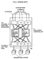
- Fig. 2 shows an arrangement of one prior art disk array.
- This includes a plurality of channel interface (IF) units 11 for execution of data transmission between a mainframe 50 and a disk array controller 2, a plurality of disk IF units 12 for execution of data transfer between HDDs 20 and the disk array control unit 2, a cache memory unit 14 for temporality storing data of HDDs 20, and a shared memory unit 15 for storing control information as to the disk array controller 2 (for example, information concerning data transfer control between the channel and disk IF units 11, 12 and the cache memory unit 14), wherein the cache memory unit 14 and shared memory unit 15 are arranged so that these are accessible from all of the channel IF units 11 and disk IF units 12.
- IF channel interface
- the channel IF unit 11 has an interface for connection with the mainframe 50 and also a microprocessor (not shown) for controlling input/output with respect to the mainframe 50.
- the disk IF unit 12 has an interface for connection to the HDDs 20 and a microprocessor (not shown ) for controlling input/output relative to HDDs 20.
- the disk IF unit 12 also executes RAID functions.
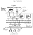
- the number of disk IF units In order to make the architecture of a disk array scalable, the number of disk IF units must be increased according to the capacity of the disk (the number of logical volumes) connected to a disk controller. In addition, the number of channel IF units in the object disk array controller must be increased according to the necessary number of channels connected to the host computer. For the disk array controller that employs the shared bus connection form, however, increasing of the number of channel IF units and disk IF units such way disables the data transfer throughput of the access path between each of the channel IF units and/or the disk IF units and a cache memory unit or a shared memory unit to become scalable according to an increase in number of channel IF units or disk IF units. This is because the shared bus becomes a bottleneck in making the access path throughput scalable.
- the disk array controller should further include a selector unit connected to the first and second channel interface units, the disk interface units, and the cache memory.
- the first and second channel interface units and the disk interface unit are connected to the selector unit through an access path respectively in a one-by-one manner.
- the selector unit and the cache memory are also connected to each other through an access path.
- the total number of access paths for the connection between the first and second channel interface units and/or the disk interface unit and the selector unit is more than the total number of access paths for the connection between the selector unit and the cache memory unit.
- the first and second channel interface units and the disk interface units are connected to the selector unit and the shared memory through an access path respectively in a one-by-one manner.
- the disk array controller should preferably be provided with a plurality of the selector units.
- the first channel interface units and the second channel interface units should be connected to different selector units respectively.
- the disk array controller of further another invention includes a first host interface group; a second host interface group; a first disk interface group; a second disk interface group; a first selector unit connected to the first host interface group and the disk interface group through the first access path; the second selector unit connected to the second host interface group and the first disk interface group through the second access path; a cache memory connected to the first and second selector groups.
- the bandwidth of the first access paths is set equally to that of the second access paths.
- Each of the first and second host interface groups should preferably include a host interface for the first type channels and a host interface for the second type channels, which is narrower than the bandwidth of the first type channels.
- Each of the first and second disk interface groups should preferably include a disk interface for the first type channels and a disk interface for the third type channels, which is narrower than the bandwidth of the first type channels.
- the disk array controller of further another invention is provided with a first selector unit, a second selector unit, and a cache memory connected to the first and second selector units.
- the first selector unit is connected to k (k: a natural number) host interface units for the first type channels; l (l: a natural number) host interfaces for the second type channels; m (m: a natural number) disk interface units for the first type channels; and n (n: a natural number) host interface units for the third type channels.
- the second selector unit is connected to k (k: a natural number) host interface units for the first type channels, which are different from the host interface units connected to the first selector unit; l (l: a natural number) host interfaces for the second type channels, which are different from the host interface units connected to the first selector unit; m (m: a natural number) disk interface units for the first type channels, which are different from the disk interface units connected to the first selector unit; and n (n: a natural number) host interface units for the third type channels, which are different from the disk interface units connected to the first selector unit.
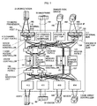
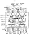
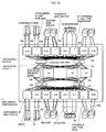
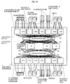
- Fig.1 is a block diagram of the disk array controller in an embodiment of the present invention.
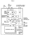
- the data transfer control unit 315 switches the selector 306 (step 504) while at the same time returning via control line(s) 2:212 to the data transfer control unit(s) 310 within the CM access control unit(s) 104 a signal (ACK) indicative of the fact that the right of connection to the access path(s) 1:136 has been obtained (step 505).
- the data transfer control unit 315 outputs via control lines 3:213 to the data transfer control unit(s) 315 within the CM controller(s) 107 a signal (REQ) indicating the start of access (step 506). Subsequently, send forth an address and command (step 507).
Landscapes
- Engineering & Computer Science (AREA)
- Theoretical Computer Science (AREA)
- Physics & Mathematics (AREA)
- General Engineering & Computer Science (AREA)
- General Physics & Mathematics (AREA)
- Human Computer Interaction (AREA)
- Computer Networks & Wireless Communication (AREA)
- Memory System Of A Hierarchy Structure (AREA)
Applications Claiming Priority (2)
| Application Number | Priority Date | Filing Date | Title |
|---|---|---|---|
| JP166899 | 1999-01-07 | ||
| JP00166899A JP4400895B2 (ja) | 1999-01-07 | 1999-01-07 | ディスクアレイ制御装置 |
Publications (3)
| Publication Number | Publication Date |
|---|---|
| EP1018686A2 true EP1018686A2 (de) | 2000-07-12 |
| EP1018686A3 EP1018686A3 (de) | 2002-03-27 |
| EP1018686B1 EP1018686B1 (de) | 2004-03-03 |
Family
ID=11507911
Family Applications (1)
| Application Number | Title | Priority Date | Filing Date |
|---|---|---|---|
| EP99126061A Expired - Lifetime EP1018686B1 (de) | 1999-01-07 | 1999-12-28 | Speicherplattenanordnung-Steuerungsvorrichtung |
Country Status (4)
| Country | Link |
|---|---|
| US (6) | US6578108B1 (de) |
| EP (1) | EP1018686B1 (de) |
| JP (1) | JP4400895B2 (de) |
| DE (1) | DE69915243T2 (de) |
Cited By (1)
| Publication number | Priority date | Publication date | Assignee | Title |
|---|---|---|---|---|
| EP1370947A4 (de) * | 2001-02-13 | 2009-05-27 | Candera Inc | Speicherungsvirtualisierungsserver auf siliciumbasis |
Families Citing this family (36)
| Publication number | Priority date | Publication date | Assignee | Title |
|---|---|---|---|---|
| JP4400895B2 (ja) * | 1999-01-07 | 2010-01-20 | 株式会社日立製作所 | ディスクアレイ制御装置 |
| JP3812928B2 (ja) * | 1999-07-14 | 2006-08-23 | 株式会社日立製作所 | 外部記憶装置及び情報処理システム |
| US6948031B2 (en) * | 2000-12-19 | 2005-09-20 | Emc Corporation | Methods and apparatus for transferring a data element within a data storage system |
| JP4039821B2 (ja) * | 2001-05-09 | 2008-01-30 | 株式会社日立製作所 | ディスク制御装置を用いた計算機システムおよびその運用サービス |
| US6973529B2 (en) * | 2001-09-28 | 2005-12-06 | International Business Machines Corporation | Multiple I/O path selection among disparate channel paths |
| US6868479B1 (en) * | 2002-03-28 | 2005-03-15 | Emc Corporation | Data storage system having redundant service processors |
| JP2003323261A (ja) * | 2002-04-26 | 2003-11-14 | Hitachi Ltd | ディスク制御システム、ディスク制御装置、ディスクシステム、及びその制御方法 |
| US7873868B1 (en) * | 2003-01-17 | 2011-01-18 | Unisys Corporation | Method for obtaining higher throughput in a computer system utilizing a clustered systems manager |
| JP2004234555A (ja) * | 2003-01-31 | 2004-08-19 | Hitachi Ltd | ストレージシステムの制御方法、ストレージシステム、及びプログラム |
| JP2004234558A (ja) * | 2003-01-31 | 2004-08-19 | Hitachi Ltd | 記憶デバイス制御装置、及びプログラム |
| JP4342804B2 (ja) * | 2003-01-31 | 2009-10-14 | 株式会社日立製作所 | ストレージシステムの制御方法、ストレージシステム、及びプログラム |
| JP4651913B2 (ja) | 2003-02-17 | 2011-03-16 | 株式会社日立製作所 | 記憶装置システム |
| JP4322031B2 (ja) | 2003-03-27 | 2009-08-26 | 株式会社日立製作所 | 記憶装置 |
| US7237021B2 (en) * | 2003-04-04 | 2007-06-26 | Bluearc Uk Limited | Network-attached storage system, device, and method supporting multiple storage device types |
| JP4060235B2 (ja) | 2003-05-22 | 2008-03-12 | 株式会社日立製作所 | ディスクアレイ装置及びディスクアレイ装置の制御方法 |
| JP2004348464A (ja) | 2003-05-22 | 2004-12-09 | Hitachi Ltd | ストレージ装置、及び通信信号の整形回路 |
| JP2005078596A (ja) * | 2003-09-03 | 2005-03-24 | Hitachi Ltd | データ転送装置の制御方法、データ転送装置、チャネル制御装置、及び記憶デバイス制御装置 |
| JP4156499B2 (ja) * | 2003-11-28 | 2008-09-24 | 株式会社日立製作所 | ディスクアレイ装置 |
| JP4497918B2 (ja) * | 2003-12-25 | 2010-07-07 | 株式会社日立製作所 | ストレージシステム |
| JP4634049B2 (ja) | 2004-02-04 | 2011-02-16 | 株式会社日立製作所 | ディスクアレイ装置における異常通知制御 |
| US7467238B2 (en) * | 2004-02-10 | 2008-12-16 | Hitachi, Ltd. | Disk controller and storage system |
| JP4405277B2 (ja) * | 2004-02-16 | 2010-01-27 | 株式会社日立製作所 | ディスク制御装置 |
| JP4441286B2 (ja) * | 2004-02-10 | 2010-03-31 | 株式会社日立製作所 | ストレージシステム |
| US9495263B2 (en) * | 2004-12-21 | 2016-11-15 | Infortrend Technology, Inc. | Redundant SAS storage virtualization subsystem and system using the same, and method therefor |
| US8301810B2 (en) * | 2004-12-21 | 2012-10-30 | Infortrend Technology, Inc. | SAS storage virtualization controller, subsystem and system using the same, and method therefor |
| JP2006268215A (ja) * | 2005-03-23 | 2006-10-05 | Hitachi Ltd | ストレージシステム |
| JP4486633B2 (ja) * | 2006-11-16 | 2010-06-23 | 株式会社日立製作所 | ディスクアレイ装置 |
| US20080162813A1 (en) * | 2007-01-02 | 2008-07-03 | International Business Machines Corporation | Multiple logic media drive |
| JP4685079B2 (ja) * | 2007-10-26 | 2011-05-18 | 株式会社日立製作所 | 記憶装置システム |
| JP2008135031A (ja) * | 2007-11-26 | 2008-06-12 | Hitachi Ltd | ディスクアレイ装置及びディスクアレイ装置の制御方法 |
| US9626127B2 (en) * | 2010-07-21 | 2017-04-18 | Nxp Usa, Inc. | Integrated circuit device, data storage array system and method therefor |
| US9690703B1 (en) * | 2012-06-27 | 2017-06-27 | Netapp, Inc. | Systems and methods providing storage system write elasticity buffers |
| US9697111B2 (en) * | 2012-08-02 | 2017-07-04 | Samsung Electronics Co., Ltd. | Method of managing dynamic memory reallocation and device performing the method |
| JP5883743B2 (ja) * | 2012-08-20 | 2016-03-15 | 株式会社日立製作所 | パケット通信網における通信途絶時間短縮方法 |
| US8898272B1 (en) | 2012-10-02 | 2014-11-25 | Amazon Technologies, Inc. | Identifying information in resource locators |
| US9678681B2 (en) * | 2015-06-17 | 2017-06-13 | International Business Machines Corporation | Secured multi-tenancy data in cloud-based storage environments |
Family Cites Families (19)
| Publication number | Priority date | Publication date | Assignee | Title |
|---|---|---|---|---|
| US5155836A (en) * | 1987-01-27 | 1992-10-13 | Jordan Dale A | Block diagram system and method for controlling electronic instruments with simulated graphic display |
| US5206939A (en) * | 1990-09-24 | 1993-04-27 | Emc Corporation | System and method for disk mapping and data retrieval |
| US5155835A (en) * | 1990-11-19 | 1992-10-13 | Storage Technology Corporation | Multilevel, hierarchical, dynamically mapped data storage subsystem |
| JPH05143242A (ja) * | 1991-11-25 | 1993-06-11 | Hitachi Ltd | 磁気デイスクシステム |
| US5237573A (en) * | 1992-03-31 | 1993-08-17 | Apple Computer, Inc. | Method and apparatus for selectively switching between input signals |
| EP0601715A1 (de) * | 1992-12-11 | 1994-06-15 | National Semiconductor Corporation | Für den On-Chip-Speicherzugriff optimierter CPV-Kernbus |
| US5476495A (en) * | 1993-03-16 | 1995-12-19 | Ep Technologies, Inc. | Cardiac mapping and ablation systems |
| JP3200500B2 (ja) | 1993-05-27 | 2001-08-20 | 株式会社日立製作所 | ディスク装置及びディスク制御方法 |
| JP3264465B2 (ja) * | 1993-06-30 | 2002-03-11 | 株式会社日立製作所 | 記憶システム |
| US5583876A (en) * | 1993-10-05 | 1996-12-10 | Hitachi, Ltd. | Disk array device and method of updating error correction codes by collectively writing new error correction code at sequentially accessible locations |
| JP3236166B2 (ja) * | 1994-06-08 | 2001-12-10 | 株式会社日立製作所 | キャッシュ制御方法および情報処理装置 |
| US5504882A (en) * | 1994-06-20 | 1996-04-02 | International Business Machines Corporation | Fault tolerant data storage subsystem employing hierarchically arranged controllers |
| US5768623A (en) * | 1995-09-19 | 1998-06-16 | International Business Machines Corporation | System and method for sharing multiple storage arrays by dedicating adapters as primary controller and secondary controller for arrays reside in different host computers |
| JP3776496B2 (ja) | 1996-01-17 | 2006-05-17 | 株式会社日立製作所 | データ記憶システム |
| JP3781212B2 (ja) | 1996-06-04 | 2006-05-31 | 株式会社日立製作所 | サブシステム |
| JP2786175B2 (ja) | 1996-11-18 | 1998-08-13 | 株式会社日立製作所 | 情報処理システム |
| JPH10333836A (ja) | 1997-05-29 | 1998-12-18 | Hitachi Ltd | ディスクアレイ制御装置 |
| JP2912299B2 (ja) * | 1997-06-10 | 1999-06-28 | 四国日本電気ソフトウェア株式会社 | ディスクアレイ制御装置 |
| JP4400895B2 (ja) | 1999-01-07 | 2010-01-20 | 株式会社日立製作所 | ディスクアレイ制御装置 |
-
1999
- 1999-01-07 JP JP00166899A patent/JP4400895B2/ja not_active Expired - Fee Related
- 1999-12-28 DE DE69915243T patent/DE69915243T2/de not_active Expired - Lifetime
- 1999-12-28 EP EP99126061A patent/EP1018686B1/de not_active Expired - Lifetime
-
2000
- 2000-01-06 US US09/478,341 patent/US6578108B1/en not_active Expired - Fee Related
-
2003
- 2003-04-07 US US10/407,456 patent/US6745287B2/en not_active Expired - Fee Related
-
2004
- 2004-04-13 US US10/822,710 patent/US6839805B2/en not_active Expired - Fee Related
- 2004-11-18 US US10/990,496 patent/US7213104B2/en not_active Expired - Fee Related
-
2006
- 2006-10-02 US US11/540,552 patent/US7318122B2/en not_active Expired - Fee Related
-
2007
- 2007-08-21 US US11/892,190 patent/US7519770B2/en not_active Expired - Fee Related
Cited By (1)
| Publication number | Priority date | Publication date | Assignee | Title |
|---|---|---|---|---|
| EP1370947A4 (de) * | 2001-02-13 | 2009-05-27 | Candera Inc | Speicherungsvirtualisierungsserver auf siliciumbasis |
Also Published As
| Publication number | Publication date |
|---|---|
| US7318122B2 (en) | 2008-01-08 |
| US7519770B2 (en) | 2009-04-14 |
| DE69915243D1 (de) | 2004-04-08 |
| US20050071552A1 (en) | 2005-03-31 |
| EP1018686B1 (de) | 2004-03-03 |
| US7213104B2 (en) | 2007-05-01 |
| US6839805B2 (en) | 2005-01-04 |
| US6745287B2 (en) | 2004-06-01 |
| US20070022247A1 (en) | 2007-01-25 |
| EP1018686A3 (de) | 2002-03-27 |
| US20040193799A1 (en) | 2004-09-30 |
| US20080010402A1 (en) | 2008-01-10 |
| US20030191892A1 (en) | 2003-10-09 |
| US6578108B1 (en) | 2003-06-10 |
| JP2000200156A (ja) | 2000-07-18 |
| DE69915243T2 (de) | 2004-10-14 |
| JP4400895B2 (ja) | 2010-01-20 |
Similar Documents
| Publication | Publication Date | Title |
|---|---|---|
| EP1018686B1 (de) | Speicherplattenanordnung-Steuerungsvorrichtung | |
| US6684295B2 (en) | Disk array control device with two different internal connection systems | |
| US7631218B2 (en) | RAID system and Rebuild/Copy back processing method thereof | |
| US7562249B2 (en) | RAID system, RAID controller and rebuilt/copy back processing method thereof | |
| US5694619A (en) | System for exclusively controlling access of a semiconductor memory module using a backup memory and compression and decompression techniques | |
| JP4477906B2 (ja) | ストレージシステム | |
| JP3946873B2 (ja) | ディスクアレイ制御装置 | |
| KR100224525B1 (ko) | 어레이 컨트롤러를 위한 채널 하드웨어 성능을 개선하기 위한 시스템 | |
| US5958078A (en) | Storage unit and storage unit subsystem | |
| US7502886B1 (en) | Data storage device with two-tier raid control circuitry | |
| US20020144028A1 (en) | Method and apparatus for increased performance of sequential I/O operations over busses of differing speeds | |
| JP2774728B2 (ja) | ディスクアレイ制御方式 | |
| JP4025032B2 (ja) | ディスク制御装置、および、そのデータアクセス方法 | |
| US7174422B1 (en) | Data storage device with two-tier raid control circuitry | |
| JP4571963B2 (ja) | ディスクアレイ制御装置 | |
| JP4452697B2 (ja) | ディスクアレイ制御装置 | |
| JP2003263278A (ja) | ディスクアレイ制御装置 | |
| JP2003263279A (ja) | ディスクアレイ制御装置 | |
| JP4485503B2 (ja) | ディスクアレイ制御装置及びディスクアレイ制御方法 | |
| JP2000010900A (ja) | ディスクアレイ制御装置、及びディスクアレイ | |
| JP2005190499A (ja) | 記憶サブシステム及び記憶制御装置 |
Legal Events
| Date | Code | Title | Description |
|---|---|---|---|
| PUAI | Public reference made under article 153(3) epc to a published international application that has entered the european phase |
Free format text: ORIGINAL CODE: 0009012 |
|
| AK | Designated contracting states |
Kind code of ref document: A2 Designated state(s): AT BE CH CY DE DK ES FI FR GB GR IE IT LI LU MC NL PT SE Kind code of ref document: A2 Designated state(s): DE FR GB |
|
| AX | Request for extension of the european patent |
Free format text: AL;LT;LV;MK;RO;SI |
|
| PUAL | Search report despatched |
Free format text: ORIGINAL CODE: 0009013 |
|
| AK | Designated contracting states |
Kind code of ref document: A3 Designated state(s): AT BE CH CY DE DK ES FI FR GB GR IE IT LI LU MC NL PT SE |
|
| AX | Request for extension of the european patent |
Free format text: AL;LT;LV;MK;RO;SI |
|
| 17P | Request for examination filed |
Effective date: 20020430 |
|
| 17Q | First examination report despatched |
Effective date: 20020919 |
|
| AKX | Designation fees paid |
Free format text: DE FR GB |
|
| GRAP | Despatch of communication of intention to grant a patent |
Free format text: ORIGINAL CODE: EPIDOSNIGR1 |
|
| GRAS | Grant fee paid |
Free format text: ORIGINAL CODE: EPIDOSNIGR3 |
|
| GRAA | (expected) grant |
Free format text: ORIGINAL CODE: 0009210 |
|
| AK | Designated contracting states |
Kind code of ref document: B1 Designated state(s): DE FR GB |
|
| REG | Reference to a national code |
Ref country code: GB Ref legal event code: FG4D |
|
| REG | Reference to a national code |
Ref country code: IE Ref legal event code: FG4D |
|
| REF | Corresponds to: |
Ref document number: 69915243 Country of ref document: DE Date of ref document: 20040408 Kind code of ref document: P |
|
| ET | Fr: translation filed | ||
| PLBE | No opposition filed within time limit |
Free format text: ORIGINAL CODE: 0009261 |
|
| STAA | Information on the status of an ep patent application or granted ep patent |
Free format text: STATUS: NO OPPOSITION FILED WITHIN TIME LIMIT |
|
| 26N | No opposition filed |
Effective date: 20041206 |
|
| PGFP | Annual fee paid to national office [announced via postgrant information from national office to epo] |
Ref country code: FR Payment date: 20130107 Year of fee payment: 14 |
|
| REG | Reference to a national code |
Ref country code: FR Ref legal event code: ST Effective date: 20140829 |
|
| PG25 | Lapsed in a contracting state [announced via postgrant information from national office to epo] |
Ref country code: FR Free format text: LAPSE BECAUSE OF NON-PAYMENT OF DUE FEES Effective date: 20131231 |
|
| PGFP | Annual fee paid to national office [announced via postgrant information from national office to epo] |
Ref country code: GB Payment date: 20141224 Year of fee payment: 16 |
|
| PGFP | Annual fee paid to national office [announced via postgrant information from national office to epo] |
Ref country code: DE Payment date: 20141223 Year of fee payment: 16 |
|
| REG | Reference to a national code |
Ref country code: DE Ref legal event code: R119 Ref document number: 69915243 Country of ref document: DE |
|
| GBPC | Gb: european patent ceased through non-payment of renewal fee |
Effective date: 20151228 |
|
| PG25 | Lapsed in a contracting state [announced via postgrant information from national office to epo] |
Ref country code: DE Free format text: LAPSE BECAUSE OF NON-PAYMENT OF DUE FEES Effective date: 20160701 Ref country code: GB Free format text: LAPSE BECAUSE OF NON-PAYMENT OF DUE FEES Effective date: 20151228 |