EP1018761A1 - Halbleiteranordnung und herstellungsverfahren dafür - Google Patents
Halbleiteranordnung und herstellungsverfahren dafür Download PDFInfo
- Publication number
- EP1018761A1 EP1018761A1 EP98938929A EP98938929A EP1018761A1 EP 1018761 A1 EP1018761 A1 EP 1018761A1 EP 98938929 A EP98938929 A EP 98938929A EP 98938929 A EP98938929 A EP 98938929A EP 1018761 A1 EP1018761 A1 EP 1018761A1
- Authority
- EP
- European Patent Office
- Prior art keywords
- semiconductor device
- electrode pads
- forming
- film
- semiconductor chip
- Prior art date
- Legal status (The legal status is an assumption and is not a legal conclusion. Google has not performed a legal analysis and makes no representation as to the accuracy of the status listed.)
- Withdrawn
Links
Images



Classifications
-
- H—ELECTRICITY
- H10—SEMICONDUCTOR DEVICES; ELECTRIC SOLID-STATE DEVICES NOT OTHERWISE PROVIDED FOR
- H10W—GENERIC PACKAGES, INTERCONNECTIONS, CONNECTORS OR OTHER CONSTRUCTIONAL DETAILS OF DEVICES COVERED BY CLASS H10
- H10W74/00—Encapsulations, e.g. protective coatings
- H10W74/01—Manufacture or treatment
- H10W74/012—Manufacture or treatment of encapsulations on active surfaces of flip-chip devices, e.g. forming underfills
-
- H—ELECTRICITY
- H10—SEMICONDUCTOR DEVICES; ELECTRIC SOLID-STATE DEVICES NOT OTHERWISE PROVIDED FOR
- H10W—GENERIC PACKAGES, INTERCONNECTIONS, CONNECTORS OR OTHER CONSTRUCTIONAL DETAILS OF DEVICES COVERED BY CLASS H10
- H10W72/00—Interconnections or connectors in packages
- H10W72/01—Manufacture or treatment
- H10W72/012—Manufacture or treatment of bump connectors, dummy bumps or thermal bumps
-
- H—ELECTRICITY
- H10—SEMICONDUCTOR DEVICES; ELECTRIC SOLID-STATE DEVICES NOT OTHERWISE PROVIDED FOR
- H10W—GENERIC PACKAGES, INTERCONNECTIONS, CONNECTORS OR OTHER CONSTRUCTIONAL DETAILS OF DEVICES COVERED BY CLASS H10
- H10W72/00—Interconnections or connectors in packages
- H10W72/20—Bump connectors, e.g. solder bumps or copper pillars; Dummy bumps; Thermal bumps
-
- H—ELECTRICITY
- H10—SEMICONDUCTOR DEVICES; ELECTRIC SOLID-STATE DEVICES NOT OTHERWISE PROVIDED FOR
- H10W—GENERIC PACKAGES, INTERCONNECTIONS, CONNECTORS OR OTHER CONSTRUCTIONAL DETAILS OF DEVICES COVERED BY CLASS H10
- H10W74/00—Encapsulations, e.g. protective coatings
- H10W74/10—Encapsulations, e.g. protective coatings characterised by their shape or disposition
- H10W74/15—Encapsulations, e.g. protective coatings characterised by their shape or disposition on active surfaces of flip-chip devices, e.g. underfills
-
- H—ELECTRICITY
- H10—SEMICONDUCTOR DEVICES; ELECTRIC SOLID-STATE DEVICES NOT OTHERWISE PROVIDED FOR
- H10W—GENERIC PACKAGES, INTERCONNECTIONS, CONNECTORS OR OTHER CONSTRUCTIONAL DETAILS OF DEVICES COVERED BY CLASS H10
- H10W72/00—Interconnections or connectors in packages
- H10W72/01—Manufacture or treatment
- H10W72/012—Manufacture or treatment of bump connectors, dummy bumps or thermal bumps
- H10W72/01215—Manufacture or treatment of bump connectors, dummy bumps or thermal bumps forming coatings
-
- H—ELECTRICITY
- H10—SEMICONDUCTOR DEVICES; ELECTRIC SOLID-STATE DEVICES NOT OTHERWISE PROVIDED FOR
- H10W—GENERIC PACKAGES, INTERCONNECTIONS, CONNECTORS OR OTHER CONSTRUCTIONAL DETAILS OF DEVICES COVERED BY CLASS H10
- H10W72/00—Interconnections or connectors in packages
- H10W72/01—Manufacture or treatment
- H10W72/012—Manufacture or treatment of bump connectors, dummy bumps or thermal bumps
- H10W72/01231—Manufacture or treatment of bump connectors, dummy bumps or thermal bumps using blanket deposition
-
- H—ELECTRICITY
- H10—SEMICONDUCTOR DEVICES; ELECTRIC SOLID-STATE DEVICES NOT OTHERWISE PROVIDED FOR
- H10W—GENERIC PACKAGES, INTERCONNECTIONS, CONNECTORS OR OTHER CONSTRUCTIONAL DETAILS OF DEVICES COVERED BY CLASS H10
- H10W72/00—Interconnections or connectors in packages
- H10W72/01—Manufacture or treatment
- H10W72/012—Manufacture or treatment of bump connectors, dummy bumps or thermal bumps
- H10W72/01251—Changing the shapes of bumps
-
- H—ELECTRICITY
- H10—SEMICONDUCTOR DEVICES; ELECTRIC SOLID-STATE DEVICES NOT OTHERWISE PROVIDED FOR
- H10W—GENERIC PACKAGES, INTERCONNECTIONS, CONNECTORS OR OTHER CONSTRUCTIONAL DETAILS OF DEVICES COVERED BY CLASS H10
- H10W72/00—Interconnections or connectors in packages
- H10W72/01—Manufacture or treatment
- H10W72/019—Manufacture or treatment of bond pads
-
- H—ELECTRICITY
- H10—SEMICONDUCTOR DEVICES; ELECTRIC SOLID-STATE DEVICES NOT OTHERWISE PROVIDED FOR
- H10W—GENERIC PACKAGES, INTERCONNECTIONS, CONNECTORS OR OTHER CONSTRUCTIONAL DETAILS OF DEVICES COVERED BY CLASS H10
- H10W72/00—Interconnections or connectors in packages
- H10W72/071—Connecting or disconnecting
- H10W72/0711—Apparatus therefor
-
- H—ELECTRICITY
- H10—SEMICONDUCTOR DEVICES; ELECTRIC SOLID-STATE DEVICES NOT OTHERWISE PROVIDED FOR
- H10W—GENERIC PACKAGES, INTERCONNECTIONS, CONNECTORS OR OTHER CONSTRUCTIONAL DETAILS OF DEVICES COVERED BY CLASS H10
- H10W72/00—Interconnections or connectors in packages
- H10W72/071—Connecting or disconnecting
- H10W72/0711—Apparatus therefor
- H10W72/07141—Means for applying energy, e.g. ovens or lasers
-
- H—ELECTRICITY
- H10—SEMICONDUCTOR DEVICES; ELECTRIC SOLID-STATE DEVICES NOT OTHERWISE PROVIDED FOR
- H10W—GENERIC PACKAGES, INTERCONNECTIONS, CONNECTORS OR OTHER CONSTRUCTIONAL DETAILS OF DEVICES COVERED BY CLASS H10
- H10W72/00—Interconnections or connectors in packages
- H10W72/071—Connecting or disconnecting
- H10W72/072—Connecting or disconnecting of bump connectors
-
- H—ELECTRICITY
- H10—SEMICONDUCTOR DEVICES; ELECTRIC SOLID-STATE DEVICES NOT OTHERWISE PROVIDED FOR
- H10W—GENERIC PACKAGES, INTERCONNECTIONS, CONNECTORS OR OTHER CONSTRUCTIONAL DETAILS OF DEVICES COVERED BY CLASS H10
- H10W72/00—Interconnections or connectors in packages
- H10W72/071—Connecting or disconnecting
- H10W72/072—Connecting or disconnecting of bump connectors
- H10W72/07231—Techniques
- H10W72/07236—Soldering or alloying
-
- H—ELECTRICITY
- H10—SEMICONDUCTOR DEVICES; ELECTRIC SOLID-STATE DEVICES NOT OTHERWISE PROVIDED FOR
- H10W—GENERIC PACKAGES, INTERCONNECTIONS, CONNECTORS OR OTHER CONSTRUCTIONAL DETAILS OF DEVICES COVERED BY CLASS H10
- H10W72/00—Interconnections or connectors in packages
- H10W72/071—Connecting or disconnecting
- H10W72/073—Connecting or disconnecting of die-attach connectors
-
- H—ELECTRICITY
- H10—SEMICONDUCTOR DEVICES; ELECTRIC SOLID-STATE DEVICES NOT OTHERWISE PROVIDED FOR
- H10W—GENERIC PACKAGES, INTERCONNECTIONS, CONNECTORS OR OTHER CONSTRUCTIONAL DETAILS OF DEVICES COVERED BY CLASS H10
- H10W72/00—Interconnections or connectors in packages
- H10W72/071—Connecting or disconnecting
- H10W72/074—Connecting or disconnecting of anisotropic conductive adhesives
-
- H—ELECTRICITY
- H10—SEMICONDUCTOR DEVICES; ELECTRIC SOLID-STATE DEVICES NOT OTHERWISE PROVIDED FOR
- H10W—GENERIC PACKAGES, INTERCONNECTIONS, CONNECTORS OR OTHER CONSTRUCTIONAL DETAILS OF DEVICES COVERED BY CLASS H10
- H10W72/00—Interconnections or connectors in packages
- H10W72/20—Bump connectors, e.g. solder bumps or copper pillars; Dummy bumps; Thermal bumps
- H10W72/221—Structures or relative sizes
- H10W72/225—Bumps having a filler embedded in a matrix
-
- H—ELECTRICITY
- H10—SEMICONDUCTOR DEVICES; ELECTRIC SOLID-STATE DEVICES NOT OTHERWISE PROVIDED FOR
- H10W—GENERIC PACKAGES, INTERCONNECTIONS, CONNECTORS OR OTHER CONSTRUCTIONAL DETAILS OF DEVICES COVERED BY CLASS H10
- H10W72/00—Interconnections or connectors in packages
- H10W72/20—Bump connectors, e.g. solder bumps or copper pillars; Dummy bumps; Thermal bumps
- H10W72/241—Dispositions, e.g. layouts
-
- H—ELECTRICITY
- H10—SEMICONDUCTOR DEVICES; ELECTRIC SOLID-STATE DEVICES NOT OTHERWISE PROVIDED FOR
- H10W—GENERIC PACKAGES, INTERCONNECTIONS, CONNECTORS OR OTHER CONSTRUCTIONAL DETAILS OF DEVICES COVERED BY CLASS H10
- H10W72/00—Interconnections or connectors in packages
- H10W72/20—Bump connectors, e.g. solder bumps or copper pillars; Dummy bumps; Thermal bumps
- H10W72/251—Materials
- H10W72/253—Materials not comprising solid metals or solid metalloids, e.g. polymers or ceramics
-
- H—ELECTRICITY
- H10—SEMICONDUCTOR DEVICES; ELECTRIC SOLID-STATE DEVICES NOT OTHERWISE PROVIDED FOR
- H10W—GENERIC PACKAGES, INTERCONNECTIONS, CONNECTORS OR OTHER CONSTRUCTIONAL DETAILS OF DEVICES COVERED BY CLASS H10
- H10W72/00—Interconnections or connectors in packages
- H10W72/30—Die-attach connectors
- H10W72/321—Structures or relative sizes of die-attach connectors
- H10W72/325—Die-attach connectors having a filler embedded in a matrix
-
- H—ELECTRICITY
- H10—SEMICONDUCTOR DEVICES; ELECTRIC SOLID-STATE DEVICES NOT OTHERWISE PROVIDED FOR
- H10W—GENERIC PACKAGES, INTERCONNECTIONS, CONNECTORS OR OTHER CONSTRUCTIONAL DETAILS OF DEVICES COVERED BY CLASS H10
- H10W72/00—Interconnections or connectors in packages
- H10W72/30—Die-attach connectors
- H10W72/351—Materials of die-attach connectors
- H10W72/352—Materials of die-attach connectors comprising metals or metalloids, e.g. solders
-
- H—ELECTRICITY
- H10—SEMICONDUCTOR DEVICES; ELECTRIC SOLID-STATE DEVICES NOT OTHERWISE PROVIDED FOR
- H10W—GENERIC PACKAGES, INTERCONNECTIONS, CONNECTORS OR OTHER CONSTRUCTIONAL DETAILS OF DEVICES COVERED BY CLASS H10
- H10W72/00—Interconnections or connectors in packages
- H10W72/30—Die-attach connectors
- H10W72/351—Materials of die-attach connectors
- H10W72/353—Materials of die-attach connectors not comprising solid metals or solid metalloids, e.g. ceramics
- H10W72/354—Materials of die-attach connectors not comprising solid metals or solid metalloids, e.g. ceramics comprising polymers
-
- H—ELECTRICITY
- H10—SEMICONDUCTOR DEVICES; ELECTRIC SOLID-STATE DEVICES NOT OTHERWISE PROVIDED FOR
- H10W—GENERIC PACKAGES, INTERCONNECTIONS, CONNECTORS OR OTHER CONSTRUCTIONAL DETAILS OF DEVICES COVERED BY CLASS H10
- H10W72/00—Interconnections or connectors in packages
- H10W72/851—Dispositions of multiple connectors or interconnections
- H10W72/853—On the same surface
- H10W72/856—Bump connectors and die-attach connectors
-
- H—ELECTRICITY
- H10—SEMICONDUCTOR DEVICES; ELECTRIC SOLID-STATE DEVICES NOT OTHERWISE PROVIDED FOR
- H10W—GENERIC PACKAGES, INTERCONNECTIONS, CONNECTORS OR OTHER CONSTRUCTIONAL DETAILS OF DEVICES COVERED BY CLASS H10
- H10W72/00—Interconnections or connectors in packages
- H10W72/90—Bond pads, in general
- H10W72/921—Structures or relative sizes of bond pads
- H10W72/923—Bond pads having multiple stacked layers
-
- H—ELECTRICITY
- H10—SEMICONDUCTOR DEVICES; ELECTRIC SOLID-STATE DEVICES NOT OTHERWISE PROVIDED FOR
- H10W—GENERIC PACKAGES, INTERCONNECTIONS, CONNECTORS OR OTHER CONSTRUCTIONAL DETAILS OF DEVICES COVERED BY CLASS H10
- H10W72/00—Interconnections or connectors in packages
- H10W72/90—Bond pads, in general
- H10W72/941—Dispositions of bond pads
- H10W72/9415—Dispositions of bond pads relative to the surface, e.g. recessed, protruding
-
- H—ELECTRICITY
- H10—SEMICONDUCTOR DEVICES; ELECTRIC SOLID-STATE DEVICES NOT OTHERWISE PROVIDED FOR
- H10W—GENERIC PACKAGES, INTERCONNECTIONS, CONNECTORS OR OTHER CONSTRUCTIONAL DETAILS OF DEVICES COVERED BY CLASS H10
- H10W72/00—Interconnections or connectors in packages
- H10W72/90—Bond pads, in general
- H10W72/951—Materials of bond pads
- H10W72/952—Materials of bond pads comprising metals or metalloids, e.g. PbSn, Ag or Cu
-
- H—ELECTRICITY
- H10—SEMICONDUCTOR DEVICES; ELECTRIC SOLID-STATE DEVICES NOT OTHERWISE PROVIDED FOR
- H10W—GENERIC PACKAGES, INTERCONNECTIONS, CONNECTORS OR OTHER CONSTRUCTIONAL DETAILS OF DEVICES COVERED BY CLASS H10
- H10W90/00—Package configurations
- H10W90/701—Package configurations characterised by the relative positions of pads or connectors relative to package parts
- H10W90/721—Package configurations characterised by the relative positions of pads or connectors relative to package parts of bump connectors
- H10W90/724—Package configurations characterised by the relative positions of pads or connectors relative to package parts of bump connectors between a chip and a stacked insulating package substrate, interposer or RDL
-
- H—ELECTRICITY
- H10—SEMICONDUCTOR DEVICES; ELECTRIC SOLID-STATE DEVICES NOT OTHERWISE PROVIDED FOR
- H10W—GENERIC PACKAGES, INTERCONNECTIONS, CONNECTORS OR OTHER CONSTRUCTIONAL DETAILS OF DEVICES COVERED BY CLASS H10
- H10W90/00—Package configurations
- H10W90/701—Package configurations characterised by the relative positions of pads or connectors relative to package parts
- H10W90/731—Package configurations characterised by the relative positions of pads or connectors relative to package parts of die-attach connectors
- H10W90/734—Package configurations characterised by the relative positions of pads or connectors relative to package parts of die-attach connectors between a chip and a stacked insulating package substrate, interposer or RDL
Definitions
- the invention relates to a semiconductor device and a method of fabricating the same. More particularly, the invention is concerned with a semiconductor device mounted on a glass substrate of a liquid crystal display panel for use as a display unit of information equipment such as televisions, computers, and so forth by the chip-on-glass (COG) method, or a semiconductor device mounted by the chip-on-board (COB) method on a printed circuit board built in electronic equipment for performing control operation, and is also concerned with a method of fabricating the same.
- COG chip-on-glass
- COB chip-on-board
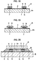
- Figs. 18 and 19 show a conventional semiconductor device, respectively, Fig. 18 being a sectional view of the conventional semiconductor device provided with straight wall bumps, and Fig. 19 a sectional view of the conventional semiconductor device provided with mushroom bumps.
- Fig. 20 is a schematic sectional view showing a condition wherein the semiconductor device shown in Fig. 18 is mounted on the glass substrate of the liquid crystal display panel with the anisotropic conductive film interposed therebetween.
- the semiconductor device 10 shown in Fig. 18 is provided with a multitude of electrode pads 2 (only two pieces thereof as enlarged are shown in the figure), made of aluminum, serving as I /O terminals, which are formed on a surface of a semiconductor chip 10a (shown in a simplified sectional view, however, a multitude of elements such as MOS transistors are in fact formed thereon).
- An insulating film 3 having an opening 3a over the respective electrode pads 2 is formed on the semiconductor chip 10a, and a plurality of the straight wall bumps 15 is provided at positions corresponding to the respective electrode pads 2 over the insulating film 3 through the intermediary of respective electrode films 12 kept in contact with the respective electrode pads 2 through the respective openings 3a.
- the semiconductor device 10 is mounted on a glass substrate 16 of a liquid crystal display panel, provided with wirings 17 patterned thereon by use of indium tin oxide (ITO) in such a way as to sandwich therebetween an anisotropic conductive film 18 containing conductive particles 19 dispersed therein.
- ITO indium tin oxide
- the bumps 15 is rendered electrically connecting with the wirings 17 by sandwiching the conductive particles 19 between the bumps 15 of the semiconductor device 10 and the wirings 17 formed on the glass substrate 16, and by applying heat and pressure thereto. Insulation between the bumps 15, adjacent to each other, can be maintained because the conductive particles 19 are not sandwiched therebetween.
- the conductive particles 19 are made up of a laminated film composed of nickel (Ni) and gold (Au), formed on a surface of an organic polymer resin, and those having a diameter in the range of 5 ⁇ m to 10 ⁇ m are in use.
- Fig. 20 for the sake of convenience in illustration, two or three pieces of the conductive particles 19 are shown to be sandwiched between the respective bumps 15 and the respective wirings 17. However, in order to secure electrical conduction with resistance at not more than 1 ⁇ , at least about ten pieces of the conductive particles 19 needs to be sandwiched therebetween.
- an upper surface area of the respective bumps 15 needs to be not less than 3000 ⁇ m 2 .
- the respective bumps 15 need to have an upper surface area not less than 3000 ⁇ m 2 , the respective bumps 15 were needed to be formed in size at 60 ⁇ m ⁇ 50 ⁇ m if the same were designed based on the assumption that the bumps 15 are arranged at an alignment pitch of 80 ⁇ m, and gap between the adjacent bumps 15 is set at 20 ⁇ m.
- the respective bumps 15 were designed to have a height (height of an upper surface of the respective bumps 15 from the surface of the insulating film 3) in the range between 10 ⁇ m and 20 ⁇ m, taking into consideration capability of the respective bumps 15 for efficiently arresting the conductive particles 19 over the top thereof, and the fact that a gap between the semiconductor device 10 and the glass substrate 16 is to be filled up with resin composing the anisotropic conductive film 18.
- the alignment pitch (connection pitch) of the bumps 15 as small as 50 ⁇ m could be accommodated.
- the mushroom bumps 25 are made up of a laminated film composed of gold (Au) or copper (Cu) and gold (Au), and are formed by means of the plating. And as with the case of the straight wall bumps, the mushroom bumps 25 are electrically connected with respective electrode pads 2 of a semiconductor chip 20a via an electrode film 12.
- a pixel pitch is required to be in the range of 20 ⁇ m to 40 ⁇ m in size.
- the conductive particles are less than 5 ⁇ m in diameter, the bumps of a semiconductor device, corresponding to the pixel pitch from 20 ⁇ m to 40 ⁇ m, can be designed. But if the conductive particles are 5 ⁇ m in diameter, it is impossible to mount the semiconductor device 10 so as to correspond to the pixel pitch as required such as from 20 ⁇ m to 40 ⁇ m because even in the case of the straight wall bumps 15, the connection pitch is 50 ⁇ m at the minimum.
- the bumps need to be formed such that a width of respective openings in a resist is not more than 10 ⁇ m to a thickness of the resist in the range of 10 ⁇ m to 20 ⁇ m.
- a tight aspect ratio of the resist ratio of the thickness to the width of the openings
- the alignment pitch is 80 ⁇ m at the minimum, and accordingly, the connection pitch needs to be designed wider relative the pixel pitch than in the case of the straight wall bumps.
- a picture-frame size of portions of the liquid crystal display unit, outside display regions thereof, needs to be enlarged, thus resulting in further depreciation of the commercial value of the liquid crystal display unit than in the case of the semiconductor device provided with the straight wall bumps.
- the bumps In the case of the mushroom bumps, it is practically impossible to form the bumps with a height in the range of 10 ⁇ m to 20 ⁇ m, corresponding to the connection pitch at 20 ⁇ m due to a structural feature of the mushroom bumps having a cap on top thereof.
- the invention has been developed to solve such problems as described above encountered by the conventional semiconductor device, and an object of the invention is to provide a semiconductor device wherein electrical connection in a packaged state is ensured and stabilized while the connection pitch can be rendered sufficiently small, and also to provide a method of fabricating the semiconductor device.
- the invention provides a semiconductor device comprising an insulating film formed on a surface of a semiconductor chip, having an opening over respective electrode pads serving as a plurality of I /O terminals of the semiconductor chip, a plurality of connecting electrodes formed on the insulating film so as to be in contact with the respective electrode pads through the respective openings, and a thermoplastic resin formed on the respective connecting electrodes, a plurality of pieces of conductive particles being contained in the respective thermoplastic resin.
- the respective connecting electrodes are preferably formed of a two-layer film made up of chromium, and copper, or a three-layer film made up of chromium, copper, and gold.
- a method of fabricating a semiconductor device according to the invention comprises the following steps from (1) to (5):
- a photosensitive resin film having thermoplasticity and containing conductive particles may be formed substantially across a surface of the metal film.
- a two-layer film composed of chromium and copper, or a three-layer film composed of chromium, copper, and gold is preferably formed by the sputtering across a surface of the semiconductor chip with the insulating film formed thereon.
- a plurality of connecting electrodes in contact with the respective electrode pads through the respective openings, having a surface area larger than the respective openings, may be formed on the insulating film by electroless plating, a thermoplastic resin may be formed on top of the respective connecting electrodes, and the conductive particles may be attached to the respective thermoplastic resins.
- thermoplastic resins containing the conductive particles on top of the respective connecting electrodes formed by the electroless plating, the step of attaching the conductive particles to the respective thermoplastic resins becomes unnecessary.
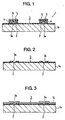
- Fig. 1 parts corresponding to those in Fig. 18 are denoted by the same reference numerals.
- the semiconductor device 1 shown in Fig. 1 is provided with a multitude of electrode pads 2 (only two pieces thereof are shown in enlarged form in the figure) serving as I /O terminals, which are formed on a surface of a semiconductor chip 1a (shown in a simplified sectional view, however, a multitude of elements such as MOS transistors are in fact formed thereon).
- An insulating film 3 is formed so as to cover a surface of the semiconductor chip 1a, and is provided with an opening 3a over the respective electrode pads 2.
- a plurality of connecting electrodes 4 is provided at positions corresponding to the respective electrode pads 2 over the insulating film 3 so as to be in contact with the respective electrode pads 2 through the respective openings 3a, and the respective connecting electrodes 4 are provided with a resin 5 having thermoplasticity, formed thereon.
- a plurality of pieces (preferably, not less than ten pieces) of conductive particles 9 (beads) is attached to or contained in an upper surface of the respective resins 5.
- the insulating film 3 is formed of a silicon nitride (SiN) film with a thickness in the range of 0.2 ⁇ m to 3 ⁇ m.
- a silicon oxide film containing impurities such as a phosphoric silicate glass (PSG), or a polyimide film which is an organic film may be used.
- a two-layer structure composed of a combination of the inorganic film as represented by the silicon nitride (SiN) film, and the organic film may be used instead.
- the respective connecting electrodes 4 are preferably formed of a single-layer metal film of gold (Au), silver (Ag), copper (Cu), and so forth, a laminated metal film composed of two layers, made of chromium (Cr) and copper (Cu), or a three-layer film made up of chromium (Cr), copper (Cu) and gold (Au). Otherwise, a two-layer film made up of titanium (Ti)-tungsten (W) alloy and gold (Au) may be used instead.
- the connecting electrode 4 is formed to a thickness in the range of 0.5 ⁇ m to 5 ⁇ m. If the connecting electrode 4 is formed to a thickness in excess of 5 ⁇ m, this is not desirable because not only time required for forming the same by the sputtering described hereinafter will be lengthened, but also time required for etching the metal film to form the connecting electrode 4 will be lengthened. Furthermore, this is not desirable also from the viewpoint of difficulty with obtaining good etching characteristics because a sidewall at opposite ends of the connecting electrode 4 tend to be in a tapered shape.
- a photosensitive resin is used in view of a method of fabricating the same as adopted, and a rubber base resist or a diazide base resist for example, THB manufactured by JSR, OMR 83 (negative resist) or OFPR 800 (positive resist) manufactured by TOKYO OHKA KOGYO CO., LTD. or the like is used.
- thermoplastic resin may suffice.
- the respective resins 5 are formed to a thickness ranging from one third to three times a diameter of the conductive particles 9 so as to enable the same to have a function of holding the conductive particles 9 to be attached thereto in the manner described later.
- the respective resins 5 have a thickness more than three times the diameter of the conductive particles 9, there arises a possibility that the shape of the respective resins 5 will collapse and the resins 5 will spread out on both sides thereof during a process of attaching the conductive particles 9 thereto in the manner as described later, thereby raising a risk of a gap between the respective connecting electrodes 4, adjacent to each other, being filled up with the resins 5.
- the gap between the respective connecting electrodes 4, adjacent to each other can not be filled up with an insulating resin (adhesive) when mounting the semiconductor device 1 on a substrate through the intermediary of the insulating resin as described later, representing an undesirable case from the viewpoint of reliability in respect of a packaged structure.
- the conductive particles 9 are spherical particles ranging from 1 ⁇ m to 15 ⁇ m in diameter, however, the diameter thereof may be not more than 5 ⁇ m.
- the conductive particles 9 are made up of a core made of a polymer resin with a laminated film composed of nickel (Ni) and gold (Au), formed on the surface of the core.
- a composition of the conductive particles 9 is not limited to the above-mentioned, and simple metal particles and alloy particles, composed of nickel (Ni), palladium (Pd) / tin (Sn), gold (Au), silver (Ag), copper (Cu), and so forth, may be used instead.
- the semiconductor device 1 is provided with the resin 5 having thermoplasticity formed on top of the respective connecting electrodes 4, direct contact of the respective connecting electrodes 4 with air can be prevented. Consequently, this enables use of a metal relatively susceptible to oxidation such as silver (Ag), copper (Cu), and so forth on the surface of the respective connecting electrodes 4, thereby enabling cost of fabrication to be reduced.
- a metal relatively susceptible to oxidation such as silver (Ag), copper (Cu), and so forth on the surface of the respective connecting electrodes 4, thereby enabling cost of fabrication to be reduced.
- the conductive particles 9 are provided on top of the respective connecting electrodes 4 by attaching the former onto the respective thermoplastic resins 5, a multitude of the conductive particles 9 can be brought into contact with wirings only at the locations where the respective connecting electrodes 4 exist when the semiconductor device 1 is mounted on the substrate by press-bonding the former with the latter. As a result, electrical connection when the semiconductor device 1 is mounted can be maintained in an excellent condition.
- uniformity in the height of the respective connecting electrodes 4 can be improved by forming the same with the use of the sputtering or the vacuum evaporation, and consequently, a condition of connection with the wirings will become highly uniform.
- the semiconductor device 1 is mounted on a glass substrate of a liquid crystal display panel, excellent display performance can be ensured.
- the semiconductor device 1 is constructed such that the conductive particles 9 are not present in any part thereof other than the connecting electrodes 4, insulation characteristics are improved if thermosetting resin, thermoplastic resin, or optosetting resin is used for the insulating resin (adhesive) at the time of mounting the semiconductor device 1.
- the conductive particles 9 are provided over the respective connecting electrodes 4 only, and none of the conductive particles 9 is sandwiched between the respective connecting electrodes 4, adjacent to each other, electrical insulation between the respective connecting electrodes 4 can be enhanced. Accordingly, excellent insulation can be maintained even if spacing between the respective connecting electrodes 4 is narrowed down, and consequently, electrical connection at a connection pitch finer than for the conventional case can be attained.
- connection pitch in the range of 20 ⁇ m to 40 ⁇ m can be accommodated.
- a method of fabricating the semiconductor device 1 shown in Fig. 1 is described hereinafter as a first embodiment of a method of fabricating a semiconductor device according to the invention.
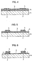
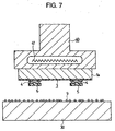
- Figs. 2 to 7 are schematic sectional views showing steps of the method of fabricating the same in sequence, and Fig. 1 shows the semiconductor device which has been completed by the method.
- an insulating film 3 having an opening 3a over respective electrode pads 2 is first formed to a thickness in the range of 0.5 ⁇ m to 5 ⁇ m on a surface of a semiconductor chip 1a provided with a plurality of the electrode pads 2 formed thereon.
- the insulating film 3 is formed of a silicon nitride (SiN) film across the surface of the semiconductor chip 1a by the plasma chemical vapor deposition (CVD). Thereafter, a photosensitive resin is applied to a surface of the SiN film, openings are formed in portions of the photosensitive resin, corresponding to the respective electrode pads 2, by use of the photolithography, and the SiN film is etched using the photosensitive resin as masks, thereby forming openings 3a.
- SiN silicon nitride
- a metal film 14 is formed to a substantially uniform thickness in the range of 0.5 ⁇ m to 10 ⁇ m across an upper surface of the insulating film 3 on the semiconductor chip 1a by use of the sputtering or the vacuum evaporation.
- the metal film 14 is formed of any of a single-layer metal film and a multiple-layer metal film, preferably a two-layer film composed of chromium and copper, a three-layer film composed of chromium, copper, and gold, or a two-layer film composed of a titanium-tungsten alloy and gold.
- the metal film 14 is in contact with the respective electrode pads 2 through the respective openings 3a of the insulating film 3.
- the metal film 14 is formed of a metal film having good intimate contact with the electrode pads 2 made of aluminum for underlayer, and is formed of a metal film having a high electric conductivity for upper layer.
- a film of a photosensitive resin 5 having thermoplasticity is formed across a surface of the metal film 14.
- patterning of the photosensitive resin 5 is performed by use of the photolithography whereby exposure and development processes are applied to the photosensitive resin 5 such that masks having a surface area larger than the respective openings 3a of the insulating film 3 are formed at portions thereof, corresponding to the respective electrode pads 2.
- the photosensitive resin 5 is patterned in such a shape as to overlap the respective openings 3a to the extent of not less than 2 ⁇ m from the periphery thereof.
- the respective portions of the photosensitive resin 5, left intact as the masks can be rendered to have a surface area equivalent to or smaller than the size of the respective openings 3a of the insulating film 3 provided that an etch selectivity between the metal film 14 and the electrode pads 2 is increased.
- a fiat plate 30 with a multitude of conductive particles 9 placed on a surface thereof at a high density is prepared.
- the semiconductor chip 1a shown in Fig. 6 is fixedly attached to the underside surface of a press heating tool 40 incorporating a heater 41 therein such that a surface of the semiconductor chip 1a with the photosensitive resins 5 formed thereon points downward.
- the semiconductor chip 1a is fixed to the press heating tool 40 by vacuum holding.
- the press heating tool 40 is caused to descend, thereby pressing the photosensitive resins 5 side of the semiconductor chip 1a against the flat plate 30.
- thermoplastic photosensitive resins 5 are softened to some extent by heat applied by the heater 41 inside the press heating tool 40, so that the multitude of the conductive particles 9 placed on the flat plate 30 can be attached to the photosensitive resins 5.
- the flat plate 30 is then loses the number of the conductive particles 9 thereof to the extent that have been attached to the photosensitive resins 5.
- the semiconductor device 1 provided with the plurality of the conductive particles 9 attached to the photosensitive resins 5 on top of the respective connecting electrodes 4 as shown in Fig. 1 is completed.
- an effective load for pressing is set in the range of 1 kg to 5 kg, heating temperature at 100°C, and a duration for heating in the range of 5 seconds to 10 seconds.
- a density at which the conductive particles 9 are placed on the flat plate 30 satisfies at least a relationship S1 >S2 ⁇ 10 provided that a surface area of the respective connecting electrodes 4 is defined S1, and a surface area of the conductive particles 9 after press-bonded as seen by projecting the same in the direction of press-bonding is defined S2.
- the metal film 14 is formed by use of the sputtering or the vacuum evaporation, and the respective connecting electrodes 4 are formed by etching the former, variation in a height thereof (film thickness) fails within 0.5 ⁇ m, and consequently, substantially uniform connecting electrodes with very small variation in thickness can be obtained.
- this embodiment wherein a plating process as required in the conventional case is not necessary has also an advantage of shortening a fabrication process.
- Fig. 8 shows in detail a step of attaching the conductive particles 9 to the respective photosensitive resins 5 in such a case.
- parts corresponding to those in Fig. 7 are denoted by the same reference numerals.
- FIG. 8 shows a flat plate 30 provided with a multitude of the conductive particles 9 placed thereon in a compact manner, and (b) shows a condition wherein a surface of a semiconductor chip 1a, on the photosensitive resins 5 side thereof, where the connecting electrodes 4 and the photosensitive resins 5 are formed, is butted against tile conductive particles 9 placed on the flat plate 30.
- (c) shows a condition wherein the semiconductor chip 1a is being pressed and heated by the press heating tool 40.
- (d) shows a condition wherein a multitude of the conductive particles 9 are caused to be attached to the respective photosensitive resins 5 after the semiconductor chip 1a is detached from the flat plate 30, thereby completing the semiconductor device 1.
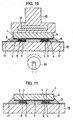
- an insulating resin (adhesive) 13 serving as a sealant is applied with the use of a dispenser to an area on a glass substrate 16 of the liquid crystal display panel, with wirings 17 patterned thereon, where the semiconductor device 1 is to be mounted. Subsequently, the wirings 17 are aligned with the connecting electrodes 4 of the semiconductor device 1, and pressure and heat are applied from the rear surface side of the semiconductor device 1 by the press heating tool 40, thereby curing the insulating resin 13.
- the photosensitive resins 5 on the respective connecting electrodes 4 are softened, so that the respective conductive particles 9 are sandwiched between the respective connecting electrodes 4 and the respective wirings 17 in such a way so as to be in contact with both.
- the respective conductive particles 9 sandwiched in-between causes electrical conduction to occur between the respective connecting electrodes 4 and the respective wirings 17, however, the conductive particles 9 which are not sandwiched therebetween maintain insulation by the photosensitive resin 5 and the insulating resin 13.
- the insulating resin 13 When using the insulating resin 13 formed in a sheet-like shape, the insulating resin 13 is disposed on the glass substrate 16 by press-bonding the same thereto with the use of the press heating tool.
- thermosetting resin or thermoplastic resin for the insulating resin 13 When using thermosetting resin or thermoplastic resin for the insulating resin 13, a light source lamp 50 shown in Fig. 10 is unnecessary, however, when using optosetting resin, the insulating resin 13 needs to be cured by irradiating the same with light by lighting up the light source lamp 50 disposed on a side of the glass substrate 16, opposite from the semiconductor device 1 while keeping the semiconductor device 1 in a pressurized condition.
- Fig. 11 shows a condition wherein the semiconductor device 1 is mounted on the glass substrate 16 in such a way as described above (that is, a packaged structure).
- the respective connecting electrodes 4 of the semiconductor device 1 and the respective wirings 17 on the glass substrate 16 are in contact with each other through the intermediary of the conductive particles 9 contained in the respective photosensitive resins 5, and consequently, are electrically connected with each other.
- the connecting electrodes 4, adjacent to each other are insulated from each other since electrical connection through the intermediary of the conductive particles 9 does not occur therebetween.
- the conductive particles 9 sandwiched between the respective connecting electrodes 4 and the respective wirings 17 undergo deformation to the extent of 5 to 50 % thereof, and by curing the insulating resin 13 while keeping the conductive particles 9 in such a deformed condition, a connection condition described above is maintained, so that excellent electrical connection can be maintained.
- the second embodiment of the invention up to steps of forming an insulating film 3 and a metal film 14 on a surface of a semiconductor chip 1a with electrode pads 2 provided thereon, is the same as the first embodiment as described with reference to Figs. 2 and 3.
- thermoplastic and photosensitive resin 6 with a multitude of conductive particles 9 mixed therein is applied to the metal film 14 formed across a surface of the semiconductor chip 1a, thereby forming a photosensitive resin film.
- patterning of the photosensitive resin 6 is performed by use of the photolithography as with the case of the first embodiment such that masks having a surface area larger than those of respective openings 3a of the insulating film 3 are formed at portions thereof, corresponding to the respective electrode pads 2 on the semiconductor chip 1a.
- connecting electrodes 4 are formed over the respective electrode pads 2.
- the semiconductor device 1 with the photosensitive resin 6 containing the conductive particles 9, provided on top of the respective connecting electrode 4, is completed. Consequently, with this embodiment, the step of attaching the conductive particles 9 to the respective photosensitive resins 5 as required in the first embodiment becomes unnecessary.
- the insulating film 3 is formed on the surface of the semiconductor chip 1a provided with the electrode pads 2 formed thereon by use of the sputtering or the vacuum evaporation.
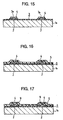
- a connecting electrode 4 made up of a metal film, composed of two layers or three layers, is formed only over the respective electrode pads 2 by electroless plating as shown in Fig. 15.
- a photosensitive resin film is formed across a surface of a semiconductor chip 1a, provided with an insulating film 3 formed thereon. and by applying exposure and development processes to the photosensitive resin film, an opening is formed at positions thereof, corresponding to the respective electrode pads 2. Subsequently, electroless plating by use of, for example, nickel (Ni) is applied using remaining portions of the photosensitive resin film as masks, thereby forming a nickel film within the respective openings only, and further, by applying gold (Au) electroless plating, a metal film is formed on top of the respective nickel films, so that the connecting electrodes 4, each made up of a two-layer metal film, are formed. Thereafter, upon removal of the remaining portions of the photosensitive resin used as the masks, the semiconductor chip 1a will be in a condition as shown in Fig. 15.
- a film of photosensitive resin 5 having thermoplasticity is formed across a surface of the semiconductor chip 1a, provided with the connecting electrode 4 formed on the respective electrode pads 2 as described above, and patterning of the photosensitive resin 5 is performed by applying exposure and development processes thereto such that portions of the photosensitive resin 5, only over the respective connecting electrodes 4, are left intact, and by attaching conductive particles 9 to respective remaining portions of the photosensitive resin 5 as with the case of the first embodiment, the same semiconductor device as that shown in Fig. 1 is completed.
- a film of photosensitive resin 6 having thermoplasticity and containing conductive particles 9 mixed therein is formed across a surface of the semiconductor chip 1a, provided with a connecting electrode 4 formed on respective electrode pads 2 as shown in Fig. 15, and patterning of the photosensitive resin 6 is performed by applying exposure and development processes thereto such that portions of the photosensitive resin 6 with the conductive particles 9 mixed therein, only over the respective connecting electrodes 4, are left intact.
- the same semiconductor device as that shown in Fig. 14 is completed.
- the semiconductor device fabricated in this way can also be securely mounted on a glass substrate or a printed circuit board through the intermediary of an insulating resin (adhesive).
- the connecting electrodes each made up of the metal film having a very high uniformity in height in comparison with the bumps of the conventional semiconductor device, are provided, and the thermoplastic resin containing the conductive particles mixed therein is provided on top of the respective connecting electrodes, so that the conductive particles can be provided beforehand at a high density only at spots where electrical connection is required. Accordingly, the conductive particles not more than 5 ⁇ m in diameter can be used. Consequently, when mounting the semiconductor device according to the invention on, for example, a glass substrate of a liquid crystal display panel, it becomes possible to implement a packaged structure with a fine connection pitch at less than 40 ⁇ m.
- the conductive particles can be prevented from spilling out because the respective connecting electrodes are formed of the metal film which can be held low in height unlike the case of the conventional bumps, so that conductive beads can be effectively arrested over the respective connecting electrodes.
- the semiconductor device according to the invention is effective for use as vanous types of semiconductor devices such as ICs for driving a liquid crystal display panel, ICs, LSIs, etc. mounted on a printed circuit board of various electronic equipment, gate arrays, and so forth.
Landscapes
- Wire Bonding (AREA)
Applications Claiming Priority (5)
| Application Number | Priority Date | Filing Date | Title |
|---|---|---|---|
| JP22477997 | 1997-08-21 | ||
| JP22477997 | 1997-08-21 | ||
| JP17851198 | 1998-06-25 | ||
| JP17851198 | 1998-06-25 | ||
| PCT/JP1998/003709 WO1999010928A1 (fr) | 1997-08-21 | 1998-08-21 | Dispositif semi-conducteur et procede de fabrication correspondant |
Publications (2)
| Publication Number | Publication Date |
|---|---|
| EP1018761A1 true EP1018761A1 (de) | 2000-07-12 |
| EP1018761A4 EP1018761A4 (de) | 2000-12-06 |
Family
ID=26498672
Family Applications (1)
| Application Number | Title | Priority Date | Filing Date |
|---|---|---|---|
| EP98938929A Withdrawn EP1018761A4 (de) | 1997-08-21 | 1998-08-21 | Halbleiteranordnung und herstellungsverfahren dafür |
Country Status (5)
| Country | Link |
|---|---|
| EP (1) | EP1018761A4 (de) |
| KR (1) | KR20010022036A (de) |
| CN (1) | CN1267395A (de) |
| AU (1) | AU8748698A (de) |
| WO (1) | WO1999010928A1 (de) |
Cited By (2)
| Publication number | Priority date | Publication date | Assignee | Title |
|---|---|---|---|---|
| EP1942365A3 (de) * | 2006-11-22 | 2009-07-01 | Samsung Electronics Co., Ltd. | Treiberschaltung für eine Flüssigkristallanzeigevorrichtung, Herstellungsverfahren dafür und Anzeigevorrichtung damit |
| US8119449B2 (en) | 2006-03-14 | 2012-02-21 | Panasonic Corporation | Method of manufacturing an electronic part mounting structure |
Families Citing this family (5)
| Publication number | Priority date | Publication date | Assignee | Title |
|---|---|---|---|---|
| JP3891133B2 (ja) * | 2003-03-26 | 2007-03-14 | セイコーエプソン株式会社 | 電子部品の製造方法および電子部品の実装方法 |
| JP2006286736A (ja) * | 2005-03-31 | 2006-10-19 | Sony Chemical & Information Device Corp | 電気部品、電気装置、及び電気部品の製造方法 |
| JP4800253B2 (ja) * | 2007-04-04 | 2011-10-26 | 新光電気工業株式会社 | 配線基板の製造方法 |
| CA3049152C (en) * | 2017-01-04 | 2024-04-02 | Shih-Hsien Tseng | Pixel unit structure and manufacturing method thereof |
| US20200185345A1 (en) * | 2018-12-07 | 2020-06-11 | Nanya Technology Corporation | Semiconductor device |
Family Cites Families (9)
| Publication number | Priority date | Publication date | Assignee | Title |
|---|---|---|---|---|
| KR910006967B1 (ko) * | 1987-11-18 | 1991-09-14 | 가시오 게이상기 가부시기가이샤 | 반도체 장치의 범프 전극 구조 및 그 형성 방법 |
| JP2596960B2 (ja) * | 1988-03-07 | 1997-04-02 | シャープ株式会社 | 接続構造 |
| JPH02280334A (ja) * | 1989-04-21 | 1990-11-16 | Citizen Watch Co Ltd | 半導体装置及びその製造方法 |
| JPH03218644A (ja) * | 1990-01-24 | 1991-09-26 | Sharp Corp | 回路基板の接続構造 |
| JPH0669278A (ja) * | 1992-08-18 | 1994-03-11 | Toshiba Corp | 半導体素子の接続方法 |
| JP2581572Y2 (ja) * | 1993-04-09 | 1998-09-21 | シチズン時計株式会社 | 液晶表示装置 |
| JP3297144B2 (ja) * | 1993-05-11 | 2002-07-02 | シチズン時計株式会社 | 突起電極およびその製造方法 |
| JPH0864637A (ja) * | 1994-08-26 | 1996-03-08 | Rohm Co Ltd | 半導体装置の製造方法 |
| JP2710234B2 (ja) * | 1995-07-31 | 1998-02-10 | 日本電気株式会社 | 端子接続方法およびこの方法により製造される回路基板 |
-
1998
- 1998-08-21 EP EP98938929A patent/EP1018761A4/de not_active Withdrawn
- 1998-08-21 CN CN98808360A patent/CN1267395A/zh active Pending
- 1998-08-21 WO PCT/JP1998/003709 patent/WO1999010928A1/ja not_active Ceased
- 1998-08-21 AU AU87486/98A patent/AU8748698A/en not_active Abandoned
- 1998-08-21 KR KR1020007000605A patent/KR20010022036A/ko not_active Ceased
Cited By (3)
| Publication number | Priority date | Publication date | Assignee | Title |
|---|---|---|---|---|
| US8119449B2 (en) | 2006-03-14 | 2012-02-21 | Panasonic Corporation | Method of manufacturing an electronic part mounting structure |
| EP1942365A3 (de) * | 2006-11-22 | 2009-07-01 | Samsung Electronics Co., Ltd. | Treiberschaltung für eine Flüssigkristallanzeigevorrichtung, Herstellungsverfahren dafür und Anzeigevorrichtung damit |
| US8576368B2 (en) | 2006-11-22 | 2013-11-05 | Samsung Display Co., Ltd. | Driving circuit for a liquid crystal display device, method of manufacturing the same and display device having the same |
Also Published As
| Publication number | Publication date |
|---|---|
| EP1018761A4 (de) | 2000-12-06 |
| AU8748698A (en) | 1999-03-16 |
| WO1999010928A1 (fr) | 1999-03-04 |
| CN1267395A (zh) | 2000-09-20 |
| KR20010022036A (ko) | 2001-03-15 |
Similar Documents
| Publication | Publication Date | Title |
|---|---|---|
| KR100352566B1 (ko) | 액티브 매트릭스 액정 표시 장치 | |
| US6232563B1 (en) | Bump electrode and method for fabricating the same | |
| TWI257650B (en) | Method for mounting semiconductor device, as well as circuit board, electrooptic device, and electronic device | |
| US8421248B2 (en) | Electronic device and electronic apparatus | |
| US6339247B1 (en) | Structure for mounting a semiconductor device on a liquid crystal display, and semiconductor device | |
| WO1999010928A1 (fr) | Dispositif semi-conducteur et procede de fabrication correspondant | |
| KR100225398B1 (ko) | 반도체 범프의 본딩구조 및 방법 | |
| CN101807554B (zh) | 电子基板及其制造方法、电光学装置、及电子设备 | |
| JP2001244366A (ja) | 半導体集積回路装置及びその製造方法 | |
| JPH11297751A (ja) | 半導体装置 | |
| JP4145902B2 (ja) | 半導体装置及びその製造方法 | |
| JP2002134541A (ja) | 半導体装置とその製造方法ならびに半導体装置の実装構造 | |
| JP2003007749A (ja) | 集積回路及び表示装置 | |
| JP2004205551A (ja) | 画像表示パネル、フォトマスク、画像表示装置、画像表示パネルを製造する方法 | |
| JPH02280334A (ja) | 半導体装置及びその製造方法 | |
| JP3283947B2 (ja) | 半導体装置およびその製造方法 | |
| JP2012079956A (ja) | 半導体装置及び半導体装置の製造方法 | |
| CN100521151C (zh) | 电子基板与其制法、电光学装置的制法及电子设备的制法 | |
| JP2002196703A (ja) | 半導体素子の実装構造及びその構造を有する液晶表示装置 | |
| JP4873144B2 (ja) | 電子デバイスの製造方法、及び、半導体装置 | |
| KR0157008B1 (ko) | 이방성 도전막을 이용한 칩형 소자의 실장방법 | |
| JPWO1999010928A1 (ja) | 半導体装置およびその製造方法 | |
| JP2008109024A (ja) | 半導体装置及び電子デバイス、並びに、電子デバイスの製造方法 | |
| JP2001358252A (ja) | 半導体装置 | |
| JP2001274193A (ja) | 半導体装置およびその製造方法 |
Legal Events
| Date | Code | Title | Description |
|---|---|---|---|
| PUAI | Public reference made under article 153(3) epc to a published international application that has entered the european phase |
Free format text: ORIGINAL CODE: 0009012 |
|
| 17P | Request for examination filed |
Effective date: 20000303 |
|
| AK | Designated contracting states |
Kind code of ref document: A1 Designated state(s): CH DE FR GB LI NL |
|
| A4 | Supplementary search report drawn up and despatched |
Effective date: 20001019 |
|
| AK | Designated contracting states |
Kind code of ref document: A4 Designated state(s): CH DE FR GB LI NL |
|
| RIC1 | Information provided on ipc code assigned before grant |
Free format text: 7H 01L 21/60 A, 7H 01L 23/485 B |
|
| 17Q | First examination report despatched |
Effective date: 20010918 |
|
| RAP1 | Party data changed (applicant data changed or rights of an application transferred) |
Owner name: CITIZEN WATCH CO. LTD. |
|
| GRAH | Despatch of communication of intention to grant a patent |
Free format text: ORIGINAL CODE: EPIDOS IGRA |
|
| RTI1 | Title (correction) |
Free format text: METHOD OF FABRICATING A SEMICONDUCTOR DEVICE |
|
| STAA | Information on the status of an ep patent application or granted ep patent |
Free format text: STATUS: THE APPLICATION IS DEEMED TO BE WITHDRAWN |
|
| 18D | Application deemed to be withdrawn |
Effective date: 20031031 |