EP1018778B1 - Antenne à microbandes multi-couches - Google Patents
Antenne à microbandes multi-couches Download PDFInfo
- Publication number
- EP1018778B1 EP1018778B1 EP99124675A EP99124675A EP1018778B1 EP 1018778 B1 EP1018778 B1 EP 1018778B1 EP 99124675 A EP99124675 A EP 99124675A EP 99124675 A EP99124675 A EP 99124675A EP 1018778 B1 EP1018778 B1 EP 1018778B1
- Authority
- EP
- European Patent Office
- Prior art keywords
- plane
- patch
- dielectric layer
- feed member
- ground plane
- Prior art date
- Legal status (The legal status is an assumption and is not a legal conclusion. Google has not performed a legal analysis and makes no representation as to the accuracy of the status listed.)
- Expired - Lifetime
Links
- 239000000758 substrate Substances 0.000 description 14
- 230000005855 radiation Effects 0.000 description 7
- 239000004020 conductor Substances 0.000 description 5
- 230000009977 dual effect Effects 0.000 description 4
- 239000000523 sample Substances 0.000 description 4
- 230000008878 coupling Effects 0.000 description 3
- 238000010168 coupling process Methods 0.000 description 3
- 238000005859 coupling reaction Methods 0.000 description 3
- 230000005684 electric field Effects 0.000 description 3
- 230000005670 electromagnetic radiation Effects 0.000 description 3
- 230000005284 excitation Effects 0.000 description 3
- 238000004519 manufacturing process Methods 0.000 description 3
- 230000010287 polarization Effects 0.000 description 3
- 238000003491 array Methods 0.000 description 1
- 230000005540 biological transmission Effects 0.000 description 1
- 238000010276 construction Methods 0.000 description 1
- 239000006185 dispersion Substances 0.000 description 1
- 230000008030 elimination Effects 0.000 description 1
- 238000003379 elimination reaction Methods 0.000 description 1
- 238000002955 isolation Methods 0.000 description 1
- 239000007769 metal material Substances 0.000 description 1
- 238000004806 packaging method and process Methods 0.000 description 1
- 230000010363 phase shift Effects 0.000 description 1
- 238000000926 separation method Methods 0.000 description 1
Images

Classifications
-
- H—ELECTRICITY
- H01—ELECTRIC ELEMENTS
- H01Q—ANTENNAS, i.e. RADIO AERIALS
- H01Q3/00—Arrangements for changing or varying the orientation or the shape of the directional pattern of the waves radiated from an antenna or antenna system
- H01Q3/44—Arrangements for changing or varying the orientation or the shape of the directional pattern of the waves radiated from an antenna or antenna system varying the electric or magnetic characteristics of reflecting, refracting, or diffracting devices associated with the radiating element
- H01Q3/46—Active lenses or reflecting arrays
-
- H—ELECTRICITY
- H01—ELECTRIC ELEMENTS
- H01Q—ANTENNAS, i.e. RADIO AERIALS
- H01Q5/00—Arrangements for simultaneous operation of antennas on two or more different wavebands, e.g. dual-band or multi-band arrangements
- H01Q5/40—Imbricated or interleaved structures; Combined or electromagnetically coupled arrangements, e.g. comprising two or more non-connected fed radiating elements
- H01Q5/42—Imbricated or interleaved structures; Combined or electromagnetically coupled arrangements, e.g. comprising two or more non-connected fed radiating elements using two or more imbricated arrays
Definitions
- This invention relates to microstrip patch antennas and to arrays of such antennas and, more particularly, to a horn fed array for the generation of shaped or pencil beams.
- lens antennas are utilized to form shaped or pencil beams.
- an array of unit cells are formed on a single lens comprising a dielectric substrate with one or more conducting layers.
- the unit cells have stripline feed members which channel electromagnetic waves.
- the stripline feed members vary in length in order to provide appropriate phase differences required to generate the shaped/pencil beam.
- the electromagnetic radiation to be received or transmitted is typically provided directly to the feed member in the form of electrical power.
- the phase versus frequency characteristic of each unit cell is preferably linear in order to maintain the desired beam shape over a range of frequencies.
- DE 42 39 597 A1 discloses a dual-polarization planar antenna which includes: a first feeding substrate having a plurality of first radiation elements and a first feeding line; a first dielectric member; a first ground conductor having a plurality of slots; a second dielectric member; a second feeding substrate having a plurality of second radiation elements and a second feeding line; a third dielectric member; and a second ground conductor.
- the first feeding substrate, the first dielectric member, the first ground conductor, the second dielectric member, the second feeding substrate, the third dielectric member, and the second ground conductor are successively superposed in this order.
- the first feeding substrate, the first ground conductor, and the second feeding substrate are arranged so that the slots, the first radiation elements, and the second radiation elements are overlapped with one another at the same positions.
- the first and the second feeding substrates are arranged so that the first radiation elements are excited by the first feeding line in a first excitation direction, while the second radiation elements are excited by a second feeding line in a second excitation direction perpendicular to the first excitation direction.
- the present invention discloses a novel horn-fed, multi-layered, patch antenna which is capable of transmitting and receiving shaped or pencil beams without the need for direct electrical connections.
- the inventive antenna includes an array of unit cells. Each unit cell includes a transmitting patch, located on a first patch plane, and a feeding patch located on a second patch plane. Interposed between these patches are two ground planes each containing corresponding slots. The ground planes are separated by feed members which further correspond with the slots of both ground planes. These components are all configured within a dielectric substrate.
- the horn In operation, the horn emits electromagnetic waves which strike the second patch plane.
- the energy is coupled between the second and first patch planes via the slots and feed members.
- the feed members vary in length, or size, in order to provide appropriate phase differences required to generate the desired shaped or pencil beams. Since the feed members propagate in the transverse electromagnetic (TEM) mode, the phase versus frequency characteristic of each unit cell (patch-slot-feed-member-slot-patch) is linear. This has the advantage of maintaining the beam shape over a range of frequencies.
- TEM transverse electromagnetic
- the ability of the present invention to couple energy from the second patch plane to the first, via slots and feed members, eliminates the drawbacks of the previous art. Specifically, direct connections are no longer necessary to couple the feed patches to the transmitting patches or the feed members.
- the present invention thus has the further advantage of eliminating the need for layer piercing probes thereby simplifying the antenna manufacture. In addition, the elimination of the probe connection enhances temperature stability.
- inventive antenna over prior art is its flat structure, and light weight, making it ideal for packaging within a satellite application.
- the linear phase versus frequency characteristics make wide band applications possible and the antenna's center-fed structure helps to eliminate dispersion problems.
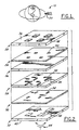
- a lens antenna structure 20 is preferred for use in a satellite 10 application as a result of its low profile and ease in which it can be configured to specialized geometries.
- Structure 20 is a horn-fed, multi-layered, printed circuit lens antenna particularly suited for shaped or pencil beams in the Ku and Ka bands.
- one embodiment of the lens antenna structure 20 is composed of a series of stacked layers.
- a first dielectric layer 22 is positioned adjacent to a first ground plane 24 which in turn is positioned adjacent to a second dielectric layer 26.
- the second dielectric layer 26 is positioned adjacent to a third dielectric layer 28 which in turn is adjacent to a second ground plane 30.
- the second ground plane 30 is positioned adjacent to a fourth dielectric layer 32.
- a feed member plane 34 Interposed between the second dielectric layer 26 and the third dielectric layer 28 is a feed member plane 34.
- positioned on a top surface 36 of the first dielectric layer 22 is a first patch plane 38, and positioned on a bottom surface 40 of the fourth dielectric layer 32 is a second patch plane 42.
- slots 50, 54 are arranged in the first and second ground planes 24, 30 respectively.
- Feed members 52 corresponding to slots 50, 54 are arranged in the third dielectric layer 28.
- the feed members 52 capacitively and electromagnetically couple the first and second patch planes 38, 42.
- a horn 44 remotely positioned below the second patch plane 42, emits electromagnetic energy in the direction of the antenna structure. This signal is received by the second patch plane 42, converted to TEM waves by the slots 50, 54 and feed members 52 in the intermediate ground planes 24, 30 and dielectric plane 28, and subsequently transmitted by the first patch plane 38.
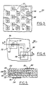
- FIG 3 is a top view of a lens antenna structure 20 in accordance with one embodiment of the present invention.
- the lens antenna structure 20 comprises a plurality of unit cells 46.
- a unit cell 46 is shown in further detail in Figure 4.
- each unit cell 46 contains a portion of the layers and planes mentioned above.
- Each unit cell 46 comprises a first patch 48 from the first patch plane 38, a top slot 50 from the first ground plane 24, a feed member 52 from the feed member plane 34, a bottom slot 54 from the second ground plane 30, and a second patch 56 from the second patch plane 42.
- Each of the elements comprising the unit cell 46 are separated by a dielectric substrate.
- patch 48 is separated from slot 50 by the first dielectric layer 22; slot 50 is separated from feed member 52 by the second dielectric layer 26; feed member 52 is separated from slot 54 by the third dielectric layer 28; and slot 54 is separated from the second patch 56 by the fourth dielectric layer 32.
- the first patch 48 is substantially centered over the top slot 50, and the second patch 56 is centered beneath the bottom slot 54.
- the first patch 48 is off-centered from the second patch 56.
- the feed member 52 has a first end 58 positioned substantially perpendicular to the top slot 50, and a second end 60 positioned substantially perpendicular to the bottom slot 54.
- the feed member ends 58 and 60 extend to, and slightly beyond, the slots 50 and 54, respectively.
- the second patch 56 receives electromagnetic energy from the horn 44.
- Patch 56 radiates a frequency band centered at the second patch 56 resonance frequency.
- This radiation induces an electric field in the bottom slot 54 which extends transversely to the long dimension of the slot 54.
- This electric field creates a TEM wave which travels along feed member 52.
- This wave induces a second electric field in the top slot 50 which, in turn, excites first patch 48 at its resonating frequency.
- First patch 48 then transmits a frequency band centered about its resonating frequency.
- the feed member 52 can be configured in different shapes.
- the feed member 52 may be straight, so that the associated top slot 50 is parallel with the associated bottom slot 54, or the feed member 52 may be bent as shown in Figure 9.
- the preferred shape of the feed member 52 is a shape which positions the first end 58 orthogonal to the second end 60.
- Such a feed member shape permits variations of feed member lengths from one unit cell 46 to the next within the same array in a spacially efficient fashion.
- the orthogonal positioning of the first end 58 to the second end 60 simplifies manufacturing and reduces associated costs since the same patch plane pattern may be utilized for both the first patch plane 38 and the second patch plane 42.
- the same ground plane pattern may be utilized for the first and second ground planes 24, 30.
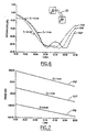
- “l” represents the distance from “s” to “s'" along the feed member 52.
- the feed member 52 propagates in the TEM mode, therefore the phase versus frequency characteristic of the unit cell 46 is linear (lines 106, 107, 108).
- the beam shape can be maintained over a range of frequencies.
- the transmitted bandwidth can be increased by using thicker substrate for the first and fourth dielectric layers 22, 32 and/or using stacked first patches 48.
- the stacked patches are approximately equal in size so as to resonate at approximately the same frequencies, but differ enough so as to broaden the bandwidth.
- the dielectric substrate utilized between stacked patches will also cause broadening of the transmitted frequency bandwidth.
- the dielectric constant is higher for the second and third dielectric layers 26, 28 than for the first and fourth dielectric layers 22, 32 in order to provide a sufficient electromagnetic coupling between the first patch 48 and the second patch 56.
- a high dielectric substrate in the feed region provides a large dynamic range for the phase.
- the lens antenna structure 20 In order to generate shaped or pencil beams, the lens antenna structure 20 must operate at appropriate phase differences. Phase differences are provided by varying the length of the feed member 52 from one unit cell 46 to the next. Figure 8 illustrates the phase shift versus feed member 52 length for a representative frequency (line 110).
- FIG. 9 shows another embodiment of a unit cell.
- a dual polarization application can be configured when utilizing a dual unit cell 62.
- Dual unit cell 62 is similar to unit cell 46 with an additional feed member 52 coupled with additional top and bottom slots 50, 54.
- the additional slots are spaced apart from, and positioned perpendicular to, the original slots. This positioning provides the preferred orthogonal coupling of electromagnetic radiation for dual polarization applications.
- the two polarizations are further isolated by a plurality of holes 64 plated with conductive metallic material connecting the respective ground planes in which slots 50 and 54 reside. To ensure proper isolation, the separation between the plurality of holes 64 is preferably less than 0.2 times the wavelength of the resonating frequency of the first and second patches 48 and 56.
- the present invention relates to an antenna structure being formed of a first patch plane, a first ground plane, a feed member plane, a second ground plane, and a second patch plane all spaced apart by layers of laminated dielectric substrate.
- a horn transmits energy upon the second patch plane.
- the energy is controlled in terms of phase and frequency, and is further electromagnetically coupled to the first patch plane which transmits in the form of shaped or pencil beams.
- the coupling between patch planes is accomplished by an array of slots located through the ground planes and an array of feed members interposed between the ground planes.
- the phase differences are established by utilization of feed members with different lengths.
Landscapes
- Physics & Mathematics (AREA)
- Electromagnetism (AREA)
- Waveguide Aerials (AREA)
- Aerials With Secondary Devices (AREA)
- Variable-Direction Aerials And Aerial Arrays (AREA)
Claims (8)
- Structure d'antenne (20), comprenant :et caractérisée par :une pluralité de cellules élémentaires (46) ayant chacune :un premier plan plaqué (38) ayant une première zone plaquée (48) ;un premier plan de masse (24) adjacent audit premier plan plaqué (38), ledit premier plan de masse (24) ayant une fente supérieure (50) en communication fonctionnelle avec ladite première zone plaquée (48) ;une première couche diélectrique (22) interposée entre ledit premier plan plaqué (38) et ledit premier plan de masse (24) ;un plan d'élément formant source primaire (34) adjacent audit premier plan de masse (24), ledit plan d'élément formant source primaire (34) ayant un élément formant source primaire (52) en communication fonctionnelle avec ladite fente supérieure (50) ;une seconde couche diélectrique (26) interposée entre ledit premier plan de masse (24) et ledit plan d'élément formant source primaire (34) ;un second plan de masse (30) adjacent audit plan d'élément formant source primaire (34) ;une troisième couche diélectrique (28) interposée entre ledit plan d'élément formant source primaire (34) et ledit second plan de masse (30) ;le fait que ledit second plan de masse (30) a une fente inférieure (54) en communication fonctionnelle avec ledit élément formant source primaire (52) ;un second plan plaqué (42) adjacent audit second plan de masse (30), ledit second plan plaqué (42) ayant une seconde zone plaquée (56) en communication fonctionnelle avec ladite fente inférieure (54) et étant apte à recevoir de l'énergie électromagnétique d'un cornet (44) ; etune quatrième couche diélectrique (32) interposée entre ledit second plan de masse (30) et ledit second plan plaqué (42).
- Structure d'antenne (20) selon la revendication 1, caractérisée en ce que ledit élément formant source primaire (52) a une première extrémité (58) positionnée perpendiculairement à, et sensiblement en dessous de, ladite fente supérieure (50), et une seconde extrémité (60) positionnée perpendiculairement à, et sensiblement au-dessus, de ladite fente inférieure (54).
- Structure d'antenne (20) selon la revendication 1 ou 2, caractérisée en chaque cellule élémentaire de ladite pluralité de cellules élémentaires (46) comporte ledit élément formant source primaire (52) ayant des longueurs variables.
- Structure d'antenne (20) selon la revendication 2, caractérisée en ce que ladite première extrémité (58) et ladite seconde extrémité (60) sont respectivement positionnées perpendiculairement l'une à l'autre.
- Structure d'antenne (20) selon l'une quelconque des revendications 1 à 4, caractérisée en ce que ledit premier plan plaqué (38) et ledit second plan plaqué (42) sont symétriquement identiques, et en ce que ledit premier plan de masse (24) et ledit second plan de masse (30) sont symétriquement identiques.
- Structure d'antenne (20) selon l'une quelconque des revendications 1 à 5, caractérisée en ce que ladite seconde couche diélectrique (26) et ladite troisième couche diélectrique (28) ont une constante diélectrique plus élevée que ladite première couche diélectrique (22) et ladite quatrième couche diélectrique (32).
- Structure d'antenne de satellite (20) selon l'une quelconque des revendications 1 à 6, caractérisée en ce que chacune de ladite pluralité de cellules élémentaires (46) comprend un second élément formant source primaire (52) et des fentes supérieure et inférieure associées (50, 54), dans laquelle lesdits éléments formant sources primaires sont séparés par une pluralité de trous (64) plaqués de façon conductrice et s'étendant à travers ladite seconde couche diélectrique (26) et ladite troisième couche diélectrique (28) afin de connecter le premier plan de masse (24) au second plan de masse (30).
- Structure d'antenne (20) selon l'une quelconque des revendications 1 à 7, caractérisée par un cornet (44) pour émettre de l'énergie sur ledit second plan plaqué (42).
Applications Claiming Priority (2)
| Application Number | Priority Date | Filing Date | Title |
|---|---|---|---|
| US220128 | 1980-12-24 | ||
| US09/220,128 US5990836A (en) | 1998-12-23 | 1998-12-23 | Multi-layered patch antenna |
Publications (2)
| Publication Number | Publication Date |
|---|---|
| EP1018778A1 EP1018778A1 (fr) | 2000-07-12 |
| EP1018778B1 true EP1018778B1 (fr) | 2003-04-02 |
Family
ID=22822189
Family Applications (1)
| Application Number | Title | Priority Date | Filing Date |
|---|---|---|---|
| EP99124675A Expired - Lifetime EP1018778B1 (fr) | 1998-12-23 | 1999-12-10 | Antenne à microbandes multi-couches |
Country Status (5)
| Country | Link |
|---|---|
| US (1) | US5990836A (fr) |
| EP (1) | EP1018778B1 (fr) |
| JP (1) | JP3314069B2 (fr) |
| CA (1) | CA2292129C (fr) |
| DE (1) | DE69906468T2 (fr) |
Families Citing this family (17)
| Publication number | Priority date | Publication date | Assignee | Title |
|---|---|---|---|---|
| US6249439B1 (en) * | 1999-10-21 | 2001-06-19 | Hughes Electronics Corporation | Millimeter wave multilayer assembly |
| US20030048226A1 (en) * | 2001-01-31 | 2003-03-13 | Tantivy Communications, Inc. | Antenna for array applications |
| US6369771B1 (en) | 2001-01-31 | 2002-04-09 | Tantivy Communications, Inc. | Low profile dipole antenna for use in wireless communications systems |
| US6417806B1 (en) | 2001-01-31 | 2002-07-09 | Tantivy Communications, Inc. | Monopole antenna for array applications |
| US6396456B1 (en) | 2001-01-31 | 2002-05-28 | Tantivy Communications, Inc. | Stacked dipole antenna for use in wireless communications systems |
| US6369770B1 (en) | 2001-01-31 | 2002-04-09 | Tantivy Communications, Inc. | Closely spaced antenna array |
| GB2403069B8 (en) | 2003-06-16 | 2008-07-17 | Antenova Ltd | Hybrid antenna using parasiting excitation of conducting antennas by dielectric antennas |
| US7071879B2 (en) * | 2004-06-01 | 2006-07-04 | Ems Technologies Canada, Ltd. | Dielectric-resonator array antenna system |
| JP2006029834A (ja) * | 2004-07-13 | 2006-02-02 | Hitachi Ltd | 車載用レーダ |
| US7098854B2 (en) * | 2004-09-09 | 2006-08-29 | Raytheon Company | Reflect antenna |
| US7656345B2 (en) * | 2006-06-13 | 2010-02-02 | Ball Aerospace & Technoloiges Corp. | Low-profile lens method and apparatus for mechanical steering of aperture antennas |
| US7595760B2 (en) * | 2006-08-04 | 2009-09-29 | Raytheon Company | Airship mounted array |
| US7605767B2 (en) * | 2006-08-04 | 2009-10-20 | Raytheon Company | Space-fed array operable in a reflective mode and in a feed-through mode |
| US7800542B2 (en) * | 2008-05-23 | 2010-09-21 | Agc Automotive Americas R&D, Inc. | Multi-layer offset patch antenna |
| JP5983760B2 (ja) * | 2012-11-07 | 2016-09-06 | 株式会社村田製作所 | アレーアンテナ |
| KR20210138418A (ko) * | 2020-05-12 | 2021-11-19 | 삼성전자주식회사 | 안테나 모듈 및 상기 안테나 모듈을 포함하는 전자 장치 |
| WO2024036550A1 (fr) * | 2022-08-18 | 2024-02-22 | 京东方科技集团股份有限公司 | Antenne, réseau d'antennes et dispositif électronique |
Family Cites Families (5)
| Publication number | Priority date | Publication date | Assignee | Title |
|---|---|---|---|---|
| JP2846081B2 (ja) * | 1990-07-25 | 1999-01-13 | 日立化成工業株式会社 | トリプレート型平面アンテナ |
| JPH0567912A (ja) * | 1991-04-24 | 1993-03-19 | Matsushita Electric Works Ltd | 平面アンテナ |
| DE4239597C2 (de) * | 1991-11-26 | 1999-11-04 | Hitachi Chemical Co Ltd | Ebene Antenne mit dualer Polarisation |
| US5394163A (en) * | 1992-08-26 | 1995-02-28 | Hughes Missile Systems Company | Annular slot patch excited array |
| US5661494A (en) * | 1995-03-24 | 1997-08-26 | The United States Of America As Represented By The Administrator Of The National Aeronautics And Space Administration | High performance circularly polarized microstrip antenna |
-
1998
- 1998-12-23 US US09/220,128 patent/US5990836A/en not_active Expired - Lifetime
-
1999
- 1999-12-10 EP EP99124675A patent/EP1018778B1/fr not_active Expired - Lifetime
- 1999-12-10 DE DE69906468T patent/DE69906468T2/de not_active Expired - Lifetime
- 1999-12-13 CA CA002292129A patent/CA2292129C/fr not_active Expired - Lifetime
- 1999-12-22 JP JP36437199A patent/JP3314069B2/ja not_active Expired - Lifetime
Also Published As
| Publication number | Publication date |
|---|---|
| CA2292129A1 (fr) | 2000-06-23 |
| JP3314069B2 (ja) | 2002-08-12 |
| JP2000196347A (ja) | 2000-07-14 |
| EP1018778A1 (fr) | 2000-07-12 |
| US5990836A (en) | 1999-11-23 |
| DE69906468D1 (de) | 2003-05-08 |
| CA2292129C (fr) | 2002-04-23 |
| DE69906468T2 (de) | 2003-10-30 |
Similar Documents
| Publication | Publication Date | Title |
|---|---|---|
| EP0447218B1 (fr) | Antenne microbande pour plusieurs fréquences | |
| US5070340A (en) | Broadband microstrip-fed antenna | |
| EP0972317B1 (fr) | Antenne reseau a microrubans | |
| EP0449492B1 (fr) | Antenne microbande dont l'uniformité de la polarisation est mise en sûreté | |
| EP1018778B1 (fr) | Antenne à microbandes multi-couches | |
| US5382959A (en) | Broadband circular polarization antenna | |
| US6535169B2 (en) | Source antennas for transmitting/receiving electromagnetic waves for satellite telecommunications systems | |
| US4929959A (en) | Dual-polarized printed circuit antenna having its elements capacitively coupled to feedlines | |
| US6545647B1 (en) | Antenna system for communicating simultaneously with a satellite and a terrestrial system | |
| US4710775A (en) | Parasitically coupled, complementary slot-dipole antenna element | |
| EP1647072B1 (fr) | Element rayonnant d'antenne a balayage electronique large bande | |
| JP3029231B2 (ja) | 二重円形偏波temモードのスロットアレーアンテナ | |
| JPH09326631A (ja) | マイクロ波平面アレイアンテナ | |
| US20040080455A1 (en) | Microstrip array antenna | |
| US5633646A (en) | Mini-cap radiating element | |
| US5233364A (en) | Dual-polarized microwave antenna element | |
| CN118315815B (zh) | 一种基于f-p谐振腔的跨频段双圆极化融合天线 | |
| Baghel et al. | SICL fed Ka-band dual polarized dipole antenna array for 5G endfire application | |
| CN1985406A (zh) | 微带阵列天线 | |
| Abd El-Rahman et al. | Dual-Band Cavity-Backed KA-band antenna for satellite communication | |
| Yang et al. | A Compact Tri-Band Dual-Circularly Polarized Shared-Aperture Antenna for Modern Internet of Vehicles | |
| CN121307504A (zh) | 一种低剖面串行馈电双频段正交极化波束可重构天线 | |
| JPH1188048A (ja) | グリッドアレイアンテナ | |
| HK1107875A (en) | Microstrip array antenna |
Legal Events
| Date | Code | Title | Description |
|---|---|---|---|
| PUAI | Public reference made under article 153(3) epc to a published international application that has entered the european phase |
Free format text: ORIGINAL CODE: 0009012 |
|
| AK | Designated contracting states |
Kind code of ref document: A1 Designated state(s): DE FR GB IT |
|
| AX | Request for extension of the european patent |
Free format text: AL;LT;LV;MK;RO;SI |
|
| 17P | Request for examination filed |
Effective date: 20001214 |
|
| AKX | Designation fees paid |
Free format text: DE FR GB IT |
|
| 17Q | First examination report despatched |
Effective date: 20010907 |
|
| GRAG | Despatch of communication of intention to grant |
Free format text: ORIGINAL CODE: EPIDOS AGRA |
|
| GRAG | Despatch of communication of intention to grant |
Free format text: ORIGINAL CODE: EPIDOS AGRA |
|
| GRAH | Despatch of communication of intention to grant a patent |
Free format text: ORIGINAL CODE: EPIDOS IGRA |
|
| GRAH | Despatch of communication of intention to grant a patent |
Free format text: ORIGINAL CODE: EPIDOS IGRA |
|
| GRAA | (expected) grant |
Free format text: ORIGINAL CODE: 0009210 |
|
| AK | Designated contracting states |
Designated state(s): DE FR GB IT |
|
| REG | Reference to a national code |
Ref country code: GB Ref legal event code: FG4D |
|
| REF | Corresponds to: |
Ref document number: 69906468 Country of ref document: DE Date of ref document: 20030508 Kind code of ref document: P |
|
| ET | Fr: translation filed | ||
| PLBE | No opposition filed within time limit |
Free format text: ORIGINAL CODE: 0009261 |
|
| STAA | Information on the status of an ep patent application or granted ep patent |
Free format text: STATUS: NO OPPOSITION FILED WITHIN TIME LIMIT |
|
| 26N | No opposition filed |
Effective date: 20040105 |
|
| REG | Reference to a national code |
Ref country code: FR Ref legal event code: PLFP Year of fee payment: 17 |
|
| REG | Reference to a national code |
Ref country code: FR Ref legal event code: PLFP Year of fee payment: 18 |
|
| PG25 | Lapsed in a contracting state [announced via postgrant information from national office to epo] |
Ref country code: IT Free format text: LAPSE BECAUSE OF NON-PAYMENT OF DUE FEES Effective date: 20151210 |
|
| PG25 | Lapsed in a contracting state [announced via postgrant information from national office to epo] |
Ref country code: IT Free format text: LAPSE BECAUSE OF NON-PAYMENT OF DUE FEES Effective date: 20151210 |
|
| PGRI | Patent reinstated in contracting state [announced from national office to epo] |
Ref country code: IT Effective date: 20170710 |
|
| REG | Reference to a national code |
Ref country code: FR Ref legal event code: PLFP Year of fee payment: 19 |
|
| PGFP | Annual fee paid to national office [announced via postgrant information from national office to epo] |
Ref country code: FR Payment date: 20181226 Year of fee payment: 20 Ref country code: GB Payment date: 20181227 Year of fee payment: 20 |
|
| PGFP | Annual fee paid to national office [announced via postgrant information from national office to epo] |
Ref country code: DE Payment date: 20181231 Year of fee payment: 20 Ref country code: IT Payment date: 20181220 Year of fee payment: 20 |
|
| REG | Reference to a national code |
Ref country code: DE Ref legal event code: R071 Ref document number: 69906468 Country of ref document: DE |
|
| REG | Reference to a national code |
Ref country code: GB Ref legal event code: PE20 Expiry date: 20191209 |
|
| PG25 | Lapsed in a contracting state [announced via postgrant information from national office to epo] |
Ref country code: GB Free format text: LAPSE BECAUSE OF EXPIRATION OF PROTECTION Effective date: 20191209 |