EP1020749A1 - Optischer wellenleiter mit mikrospiegel, sein herstellungsverfahren, und optischer signalprozessor - Google Patents
Optischer wellenleiter mit mikrospiegel, sein herstellungsverfahren, und optischer signalprozessor Download PDFInfo
- Publication number
- EP1020749A1 EP1020749A1 EP98945563A EP98945563A EP1020749A1 EP 1020749 A1 EP1020749 A1 EP 1020749A1 EP 98945563 A EP98945563 A EP 98945563A EP 98945563 A EP98945563 A EP 98945563A EP 1020749 A1 EP1020749 A1 EP 1020749A1
- Authority
- EP
- European Patent Office
- Prior art keywords
- optical waveguide
- substrate
- clad layer
- salient
- optical
- Prior art date
- Legal status (The legal status is an assumption and is not a legal conclusion. Google has not performed a legal analysis and makes no representation as to the accuracy of the status listed.)
- Granted
Links
Images


Classifications
-
- G—PHYSICS
- G02—OPTICS
- G02B—OPTICAL ELEMENTS, SYSTEMS OR APPARATUS
- G02B6/00—Light guides; Structural details of arrangements comprising light guides and other optical elements, e.g. couplings
- G02B6/02—Optical fibres with cladding with or without a coating
-
- G—PHYSICS
- G02—OPTICS
- G02B—OPTICAL ELEMENTS, SYSTEMS OR APPARATUS
- G02B6/00—Light guides; Structural details of arrangements comprising light guides and other optical elements, e.g. couplings
- G02B6/24—Coupling light guides
- G02B6/42—Coupling light guides with opto-electronic elements
- G02B6/4201—Packages, e.g. shape, construction, internal or external details
- G02B6/4246—Bidirectionally operating package structures
-
- G—PHYSICS
- G02—OPTICS
- G02B—OPTICAL ELEMENTS, SYSTEMS OR APPARATUS
- G02B6/00—Light guides; Structural details of arrangements comprising light guides and other optical elements, e.g. couplings
- G02B6/10—Light guides; Structural details of arrangements comprising light guides and other optical elements, e.g. couplings of the optical waveguide type
- G02B6/12—Light guides; Structural details of arrangements comprising light guides and other optical elements, e.g. couplings of the optical waveguide type of the integrated circuit kind
- G02B6/122—Basic optical elements, e.g. light-guiding paths
-
- G—PHYSICS
- G02—OPTICS
- G02B—OPTICAL ELEMENTS, SYSTEMS OR APPARATUS
- G02B6/00—Light guides; Structural details of arrangements comprising light guides and other optical elements, e.g. couplings
- G02B6/10—Light guides; Structural details of arrangements comprising light guides and other optical elements, e.g. couplings of the optical waveguide type
- G02B6/12—Light guides; Structural details of arrangements comprising light guides and other optical elements, e.g. couplings of the optical waveguide type of the integrated circuit kind
- G02B2006/12083—Constructional arrangements
- G02B2006/12104—Mirror; Reflectors or the like
-
- G—PHYSICS
- G02—OPTICS
- G02B—OPTICAL ELEMENTS, SYSTEMS OR APPARATUS
- G02B6/00—Light guides; Structural details of arrangements comprising light guides and other optical elements, e.g. couplings
- G02B6/24—Coupling light guides
- G02B6/42—Coupling light guides with opto-electronic elements
- G02B6/4201—Packages, e.g. shape, construction, internal or external details
- G02B6/4204—Packages, e.g. shape, construction, internal or external details the coupling comprising intermediate optical elements, e.g. lenses, holograms
- G02B6/4214—Packages, e.g. shape, construction, internal or external details the coupling comprising intermediate optical elements, e.g. lenses, holograms the intermediate optical element having redirecting reflective means, e.g. mirrors, prisms for deflecting the radiation from horizontal to down- or upward direction toward a device
Definitions
- the present invention relates to an optical waveguide to be used for connecting integrated circuits, a manufacturing method thereof, and an optical information processing apparatus that propagates an optical signal through the optical wave.
- a technique of optical interconnection in which, in order to transmit and receive a signal between a plurality of integrated circuits, an electric signal is once converted into an optical signal and the optical signal is transmitted and received, is disclosed in a document, Jpn. J. Appl. Phys. Vol. 36 (1997) pp. 1903 - 1906.
- the document discloses structure in which an electric signal is propagated through an optical waveguide on a substrate.
- a light emitting diode and a photodetector are provided to an LSI substrate for conversion between an electric signal and an optical signal, and this LSI substrate is mounted on a substrate in which an optical waveguide is formed.
- the optical signal that propagates through the optical waveguide is deflected by a micro mirror provided within the optical waveguide into a perpendicular direction to the substrate surface so as to be emitted from the optical waveguide.
- This optical signal is received by the photodetector on the LSI substrate.
- an optical signal emitted from the light emitting diode toward the optical waveguide is deflected by the micro mirror provided within the optical waveguide into the propagating direction in the optical waveguide, so as to propagate through the optical waveguide.
- a mountain-shaped aluminum mirror formed on a lower surface of the waveguide is used. Light is reflected by an inclined surface of the mountain-shaped aluminum mirror so as to be deflected.
- input and output signals of an LSI are converted into optical signals, and accordingly, they can be transmitted through an optical waveguide, while the power-supply voltage should still be supplied to the LSI, light emitting diodes, and photodetectors. This causes a problem of where lines for supplying power-supply voltage should be arranged.
- a first object of the present invention is to provide a manufacturing method for easily manufacturing an optical waveguide provided with a micro mirror within the inside so that propagated light is received/emitted downward/upward by/from a substrate surface.
- a second object of the present invention is to provide an optical waveguide in which multistage micro mirrors are provided to receive/emit propagated light downward/upward by/from a substrate surface, and intensity of light reflected by a micro mirror in a later stage can be held in a certain degree or more.
- a third object of the present invention is to provide an optical information processing apparatus constructed such that a substrate formed with electric circuits and light receiving/emitting elements is mounted on an optical waveguide substrate, while lines for power supply to the electric circuits etc. can be arranged efficiently and compactly.
- the present invention provides a following manufacturing method of an optical waveguide:
- the present invention provides a following optical waveguide
- the present invention provides a following optical information processing apparatus:
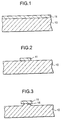
- a resist film 11 of about 1 ⁇ m in thickness is first formed on a silicon substrate 10.
- the resist film 11 is formed by spreading a photosensitive resin solution having viscosity of 20 cp (OFPR-800 made by Tokyo Ohka Kogyo Co., Ltd.) is spread at 1500 rpm for 2 seconds, and at 3000 rpm for 30 seconds using a spinner, followed by curing, to form the resistfilm 11.
- patterning is effected by exposure and development produce a shape such as shown in Fig. 2.
- a developer one containing 2.38 % of tetramethylammonium hydroxide (NMD-3 made by Tokyo Ohka Kogyo Co., Ltd.) is used.
- the silicon substrate 10 is etched using the resist film 11 as a mask and an isotropic etchant for etching the silicon substrate 10, so as to form a salient 15 of about 0.5 ⁇ m in height (Fig. 3).
- the resist film 11 is removed, and the whole surface of the silicon substrate 10 is subjected to thermal oxidation at 1100° C for 6 hours, to form an oxide film of about 1.2 ⁇ m in thickness (Fig. 4).
- This oxide film becomes a lower clad 12.
- an aluminum film 13 of 0.2 ⁇ m in thickness is formed by sputter deposition (Fig. 5). Thereafter, the aluminum film 13 is removed by photolithography, leaving the part that covers the inclined surfaces of the salient 15. By this, a micro mirror made of the aluminum film 13 is constructed.
- ultrathin coating of an organozirconium compound is formed on the order of molecule in thickness.
- organozirconium compound coating is formed to improve adhesion strength between the lower clad 12 and a polyimide optical waveguide 14 to be formed on this coating.
- OPI-N3505 made by Hitachi Chemical Co., Ltd. is coated and baked to form a polyimide layer of a desired thickness, and thereafter, as shown in Fig. 8, the polyimide layer is dry etched to have a shape of a ridge wavegguide to form an optical waveguide 14 of polyimide.
- this optical waveguide 14 propagates light utilizing air as an upper clad. A part of the propagated light is deflected upward from the silicon substrate 10 by one inclined surface 13a of the micro mirror of the aluminum film 13 to be emitted upward from the optical waveguide 14. Accordingly, by arranging a substrate 100 mounted with LSI 103, a photodetector 101 and a light emitting diode (a light emitting element including, for example, a laser diode, in addition to LED) over the silicon substrate 10, a part of the propagated light from the optical waveguide 14 can be received by the photodetector 101. By this, the optical signal being formed of the propagated light can be converted into an electric signal, which can be processed in the LSI 103.
- a light emitting diode a light emitting element including, for example, a laser diode, in addition to LED
- an electric signal outputted from the LSI 103 can be converted into an optical signal by the light emitting diode 102, and emitted toward the micro mirror of the aluminum film 13, so that it is reflected by the other inclined surface 13b of the aluminum film 13 to be deflected into the propagating direction in the optical waveguide 14. Accordingly, the electric signal outputted from the LSI 103 can be transmitted through the optical waveguide 14.
- utilization of the under-etching by isotropic etching can easily form a salient having inclined surfaces suited for a micro mirror. Accordingly, by coating a metal film on this salient, an optical waveguide 14 provided with a micro mirror can be easily manufactured. Further, the shape of the formed salient can be controlled by changing etching conditions for the isotraopic etching. Thus, it is possible to manufacture a micro mirror that deflects light in a desired direction, by controlling an angle of an inclined surface of the salient in accordance with a mode of the light propagated through the optical waveguide.
- an aluminum film 13 is employed to construct a micro mirror.
- a film of other metal such as Cr, Cu, Au, or Ag, for example, may be employed, of course.
- a dielectric film that reflects propagated light may be employed.
- a micro mirror with the salient 15 only, without particularly providing a reflecting film such as a metal film, by making the refractive index of the salient 15 smaller than the refractive index of the optical waveguide 14 and adjusting the angle of the formed inclined surface of the salient 15. In that case, it is possible to form a total reflection micro mirror by adjusting the angle of the inclined surface of the salient 15 in accordance with the refractive indexes of the optical waveguide 14 and the salient 15.
- thermal oxidation is employed to form the oxide film that makes the lower clad 12.
- CVD, sputtering etc. may be employed to form an SiO 2 film or the like on the substrate 10, the formed film serves as the lower clad 12. In that case, a thick lower clad 12 can be easily formed.
- the lower clad 12 may be formed by coating an SOG (Spin On Glass) film and curing it.
- the lower clad 12 may be formed of resin that has a smaller refractive index than that of the waveguide 14. In that case, the lower clad 12 can be formed at reduced costs.
- the salient 15 is formed on the surface of the substrate 10, and then lower clad 12 is formed to copy it in shape so that the salient 15 is formed on the surface of the lower clad 12.
- a salient may be directly formed on the surface of the lower clad 12 by forming the lower clad 12 on a flat substrate 10, and thereafter subjecting the surface of the lower clad 12 to isotropic etching.
- the substrate 10 may be formed thereon with power lines for supplying driving power to current to the LSI 103, the light emitting diode 102 and the photodetector 101, and ground lines and electric wiring for transmitting electric signals outputted from these elements, as described below.
- patterning may be carried out to form a desired pattern such as the power lines, the ground lines, and the wiring, at the same time with the patterning of the aluminum film 13 into the shape of the micro mirror.
- the micro mirror and the wiring are manufactured together.
- the micro mirror may be formed as a part of a line that crosses the optical waveguide 14.
- a metal film is subjected to isotropic etching in order to form a micro mirror having inclined surfaces.
- an SiO 2 film is made on the silicon substrate 10 to form the lower clad 21, and thereafter, an aluminum film 22 is formed on it (Fig. 10).
- a resist film 23 is formed and patterning is carried out (Fig. 11).
- This resist film 23 is used as a mask for carrying out etching of the aluminum film 22 using an etchant for isotropic etching.
- the etchant goes round to the part under the resist film 23 to cause under-etching, and accordingly, a micro mirror of a convex-shaped aluminum film 22 having inclined surfaces can be formed.
- the surface of the lower clad 21 is processed with an OPI coupler by a method similar to the first embodiment, and then, an optical waveguide 14 of polyimide is formed.
- this method directly carries out isotropic etching of the aluminum film 22, it is possible to obtain flat lower clad 21 and accordingly to improve the propagation efficiency.
- the lower clad 21 can be formed of an organic resin such as polyimide.
- the present embodiment utilizes anisotropic etching to make a salient having inclined surfaces on a substrate.
- the manufacturing method according to the present third embodiment is almost similar to that of the first embodiment, it uses a silicon substrate 10 having a (100) plane as its surface.
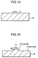
- a resist film 11 is formed as shown in Fig. 14, and potassium hydroxide solution is used as an etchant, then it is possible to form a salient 25 having inclined surfaces of (111) planes as its side faces, utilizing the characteristic that the etching rate of the (111) plane of the silicon crystal is much slower than the etching rate of the (100) plane.
- the processes thereafter are similar to those of the first embodiment.
- the angle of the (111) plane as the inclined surface is accurately decided as 54.7° with the (100) plane of the substrate surface, and accordingly, it is possible to eliminate dispersion of the inclined surface of the micro mirror.
- the mode of the optical waveguide it is possible to deflect light in a desired direction with better accuracy.
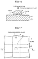
- each optical waveguide of the above-described embodiments is constructed to utilize air as an upper clad.
- a waveguide may be constructed to have an upper clad 17.
- the upper clad 17 may be used an SiO 2 film formed by sputtering or a layer of organic resin such as a polyimide layer formed by coating OPI-N1005 made by Hitachi Chemical Co., Ltd. and baking it.
- the convex-shaped micro mirror is formed under the optical waveguide 14. Accordingly, the optical waveguide 14 becomes also convex at this part.
- polishing the upper surface of the optical waveguide 14 it is possible to form a waveguide 14 that is flat in its upper surface, as shown in Fig. 18. In that case, there is effect that propagation loss of the optical waveguide 14 can be decreased.
- wet etching is employed as the isotropic etching.
- the present invention is not limited to the wet etching, and dry etching may be employed on the conditions that isotropic etching can be carried out to cause undercut.
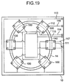
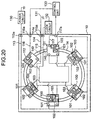
- a ring-shaped optical waveguide 14 is formed on the silicon substrate 10. Further, the substrate 10 is mounted thereon with six LSI substrates 100, 111 and 112 in total, along the optical waveguide 14. As shown in Fig. 21, in the four corners of a surface of each LSI substrate 100, 111, 112, aluminum pads 121 are formed. Also on the substrate 10, aluminum pads 122 are formed in the positions opposed to the aluminum pads 121. These are connected by copper bumps 124 through chromium films 123 and conductive adhesive layers 142. By this, the substrates 100, 111 and 112 are mounted on the substrate 10 leaving a thin gap between them. Here, the chromium film 123 is placed for enhancing the adhesive strength between the copper bump 124 and the aluminum pad 122.
- a power line 113 on the substrate 10, are formed a power line 113, a ground line 114, a clock signal line 115, and input/output signal lines 116, 117, in addition to the optical waveguide 14.
- the power line 113, the ground line 114, and the clock signal line 115 are respectively connected to aluminum pads 122 in the four corners under each of the substrate 100, 111 and 112.
- the input signal line 116 is connected to the aluminum pad 122 of the substrate 112, and the output signal line 117 is connected to the aluminum pad 122 of the substrate 111.
- power, ground, clock signal and input/output signals are supplied to the substrates 100, 111 and 112 through the copper bumps 124 and the aluminum pads 121.
- the power line 113, the ground line 114, the clock signal line 115 and the input/output signal lines 116, 117 are respectively formed with connecting pads 113a, 114a, 115a, 116a, 117a at their ends on the opposite sides to the aluminum pads 121.
- the connecting pad 113a is connected to a power circuit 130, the connecting pad 114a to ground 131, and the connecting pad 115a to a clock circuit 132.
- the connecting pads 116a, 117a are connected to a control unit 133.
- Fig. 19 shows schematic wiring paths for the sake of easy understanding of the paths of wiring 113 etc. on the substrate 10. However, practical wiring paths are decided to be effective for leading the line 113 etc. Further, although not shown in Figs. 19 and 21, a protective coat is formed on the line 113 etc.
- the four LSI substrates 100 are each mounted with a light emitting diode 102, a photodetector 101 and an LSI 103.
- the LSI substrate 111 is not mounted with a light emitting diode, but with a photodetector 101 and an LSI 103.
- the LSI substrate 112 is not mounted with a photodetector, but with a light emitting diode 102 and an LSI 103.
- each of the light emitting diodes 102 and the photodetectors 101 is mounted on the substrates 100. 111 and 112 such that its light receiving/emitting surface is located just above the optical waveguide 14 and the light receiving/emitting surface faces the optical waveguide 14.
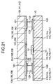
- lines 134 are arranged for supplying the power-supply voltage and the ground voltage to the light emitting diode 102, the photodetector 101 and the LSI 103 and for inputting the clock signal to the LSI 103.
- Those voltage is supplied from the side of the substrate 10 through the copper bumps (Fig. 22A).
- a line 134 for inputting the output of the photodetector 101 to the LSI 103 and a line 134 for inputting the output of the LSI to the light emitting diode 102 are arranged.
- the LSI substrate 112 is formed with lines 135 for supplying the power-supply voltage and the ground voltage to the light emitting diode 102 and the LSI 103 and for inputting the clock signal to the LSI 103 (Fig. 22B). Further, the substrate 112 is not mounted with a photodetector, and accordingly, a line 135 for inputting an input signal from the external control unit 133 to the LSI 103 is arranged.
- the LSI substrate 111 is formed with lines 136 for supplying the power-supply voltage and the ground voltage to the photodetector 101 and the LSI 103 and for inputting the clock signal to the LSI 103 (Fig. 22C). Further, in the substrate 111, is arranged a line 136 for outputting the output signal of the LSI 103 to the external control unit 133.
- the optical waveguide 14 is provided with a micro mirror of an aluminum film 13 in a position opposed to the six substrates 100, 111 and 112 (Fig. 9).
- This micro mirror has two inclined surfaces 13a, 13b along the direction of propagation of the optical waveguide 14, and deflects a part of the propagated light upward from the substrate 10 by means of one inclined surface 13a.
- the other inclined surface 13b deflects the light emitted from the light emitting diode 102, into the direction of propagation of the optical waveguide 14 so that the optical waveguide 14 propagates it.
- the power-supply voltage is supplied from the power circuit 130 through the connecting pad 113a, the power line 113 and the aluminum pads 122 on the substrate 10, and thereafter the copper bumps 124, reaching the six LSI substrates 100. 111, 112, and being supplied to the light emitting diodes 102, the photodetectors 101, and the LSIs 103 through the lines 134, 135, 136 on these substrates 100, 111, 112.
- the ground voltage is supplied through the connecting pad 114a, the ground lines 114 and the aluminum pads 122 on the substrate 10, and the copper bumps 124, the aluminum pads 121 and the lines 134, 135, 136, being supplied to the light emitting diodes 102, the photodetectors 101, and the LSIs 103.
- the clock signal outputted from the clock circuit 132 is supplied to the LSIs 103 through the clock signal line 115 on the substrate, the copper bumps 124, etc.
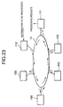
- Each of the LSIs 103 on the tour substrates 100 is connected to the photodetector 101 and the light emitting diode 102, and thus converts a signal to be sent to and received from the LSI 103 of other substrate 100.
- 111 or 112 into an optical signal, to send and receive it through the optical waveguide 14.
- the substrate 111 is not mounted with a light emitting diode, and therefore, although the LSI 103 of the substrate 111 can utilize the photodetector 101 for receiving an optical signal from the LSI 103 on other substrate 100 or 112 through the optical waveguide 14, it delivers the result of processing the received signal as the electric signal itself to the control unit 133. Further, the substrate 111 is not mounted with a photodetector.
- the LSI 103 of the substrate 111 processes a signal received as an electric signal from the control unit 133, the LSI 103 converts it into an optical signal by means of the light emitting diode 102 and then outputs it to the LSI on other substrate 100 or 111.
- the electric signal is sent to or received from the control unit 133 through the copper bumps 124, and the signal lines 116, 117 on the substrate 10.
- the LSI 103 of the substrate 100 comprises a selection circuit, an arithmetic circuit, and a signal output circuit.
- the selection circuit selects only a signal sent to itself out of signals received by the photodetector 101.
- the arithmetic circuit carries out predetermined operation using the signal selected by the selection circuit.
- the signal output circuit creates a signal that is the processing result of the arithmetic circuit added with a destination signal indicating the LSI 103 on the substrate 111, and makes the light emitting diode 102 output it as an optical signal.
- the LSI 103 of the substrate 112 comprises an information dividing circuit and a signal output circuit.
- This information dividing circuit receives information to be processed, from the control unit 133, divides the information into four pieces of information, and assigns them to the LSIs of the four substrates 100, one by one.
- the signal output circuit creates a signal that is the divided piece of information added with a destination signal indicating an assigned destination, and makes the light emitting diode 102 output it as an optical signal.
- the LSI 103 of the substrate 111 comprises a selection circuit and an output circuit.
- the selection circuit selects only a signal sent to itself out of signals received by the photodetector 101.
- the output circuit synthesizes received signals to output the result to the control unit 133.
- the LSI 103 of the substrate 112 receives information to be processed, as an electric signal from the control unit 133.
- the information dividing circuit of the LSI 103 of the substrate 112 divides the received information into four pieces of information, and decides substrates to which the divided pieces of information are assigned one by one.
- the signal output circuit of the LSI 103 of the substrate 112 creates signals obtained from the four pieces of information by respectively adding destination signals specifying assigned substrates 100, and makes the light emitting diode 102 output them as optical signals.
- the light emitted from the light emitting diode 102 of the substrate 112 is deflected by the micro mirror of the aluminum film 13 under the substrate 112, so that it becomes propagated light in the optical waveguide 14 to be propagated through the optical waveguide 14.
- the optical signals of the four pieces of information are each propagated through the optical waveguide. When they arrive at a position under the substrate 100 closest to the substrate 112, a part of the propagated light is deflected upward from the substrate 10 by the micro mirror of the aluminum film 13, as shown in Fig. 9, received by the photodetector on the substrate 100, converted into electric signals, and delivered to the LSI 103.
- the selection circuit of the LSI 103 of the substrate 100 selects only a signal of the information destined to itself out of the received electric signals, and the arithmetic circuit processes the information.
- the signal output circuit creates a signal by adding a destination signal indicating the LSI 103 of the substrate 111 to the result of the processing, and makes the light emitting diode 102 output it as an optical signal.
- the light emitted from the light emitting diode 102 of the substrate 100 is deflected by the mirror of the aluminum film 13 under the substrate 100, so that it becomes propagated light in the optical waveguide 14 to be propagated through the optical waveguide 14.
- a part of light propagated through the optical waveguide 14 is deflected by the micro mirror, so that it is received by the photodetector 101 and delivered to the LSI 103 of that substrate 100.
- the LSI 103 of that substrate 100 selects only a signal destined to itself out of the received signals, processes it, and creates a signal by adding a destination signal indicating the LSI 103 of the substrate 111 to the result of the processing, and makes the light emitting diode 102 output it as an optical signal.
- This optical signal becomes propagated light in the optical waveguide 14 to be propagated through the optical waveguide 14.
- a part of the light propagated through the optical waveguide 14 is deflected by the micro mirror, received by the photodetector 101, and delivered to the LSI 103 of the substrate 111.
- the selection circuit of the LSI 103 of the substrate 111 selects only the signals of the information destined to itself out of the delivered signals, so that it receives the respective results of processing by the LSIs 103 of the four substrates 100. A desired result of processing is obtained by synthesizing those results, and the output circuit delivers it as an electric signal to the control unit 133.
- the optical information processing system employs the ring-shaped optical waveguide 14, and thus, information circulates through the optical waveguide 14, making a loop. Accordingly, information outputted from a certain substrate can be received by all the substrates.
- the present embodiment is furnished with six substrates 100, 111, 112.
- the present embodiment has shown the construction in which the LSI substrate 112 receives information to be processed as an electric signal, the LSI substrates 100 process it in a distributed manner, and the LSI substrate 111 synthesizes the processing results and outputs the synthesized result.
- the present invention is not limited to this construction, and, of course, can employ a construction where the LSI substrates 100 send and receive processing results between them.
- the LSI substrates 100 may be employed a construction where information is received as an optical signal from an optical waveguide connected to the optical waveguide 14, or a construction where the processing result is outputted as an optical signal to the outside.
- all the LSI substrates may be constructed such that each of them is provided with a light emitting diode 102 and a photodetector 101 such as the substrates 100.
- supply of power-supply voltage etc. to the LSI substrates 100, 111 and 112 is carried out through the lines 113 etc. provided on the substrate 10 and the copper bumps supporting the LSI substrates 100, etc. Owing to such construction, power supply to the substrates 100, 111, 112 etc. mounted with the light emitting diodes 102 and the photodetectors 101 on their undersurfaces can be carried out from the side of the undersurface similarly to a flip chip. By this, it is not necessary to provide wiring and terminals on the upper sides of the substrates 100, 111 and 112. Further, fixing of the substrates 100, 111 and 112 on to the substrate 10 and electric connection can be realized at the same time by means of the copper bumps, thus simplifying the manufacturing processes.
- the lines 113 etc. are arranged on the substrate 10, and thus, the process of forming the line 113 can be carried out in a series of processes including the process of forming the micro mirrors of the aluminum film 13 and the process of forming the optical waveguide 14 etc.
- the manufacturing processes of forming the optical waveguide 14, the micro mirrors, the lines 113, etc. on the substrate 10 will be described.
- the lower clad is formed on the substrate 10 of Fig. 19, and, at the same time, the micro mirrors each consisting of the aluminum film 13 and the salient 15 are formed in positions located under the substrates 100, 111 and 112.
- the lines 113, 114, 115, 116 and 117, the aluminum pads 122, and the connecting pads 113a, 114a, 115a, 116a and 117a are formed with aluminum films of 0.8 ⁇ m in thickness by the lift-off technology.
- PIX-1400 made by Hitachi Chemical Co., Ltd. is coated and baked, in order to form protective coat 140 of polyimide all over the surface (Fig. 14).
- the protective coat 140 is removed by dry etching from the area in which the optical waveguide 14 is to be formed, and the areas of the aluminum pads 122 and the connecting pads 113a etc.
- OPI coupler made by Hitachi Chemical Co., Ltd. is coated on the surface of the lower clad 12 in the area in which the optical waveguide 14 is to be formed, to form a very thin organic molecular coat of the OPI coupler on the order of molecule in thickness.
- Such organic molecular coat of the OPI coupler is formed in order to improve adhesion strength between the optical waveguide 14 of polyimide and the lower clad 12.
- OPI-N3505 made by Hitachi Chemical Co., Ltd. is coated and baked to form a polyimide layer of a desired thickness
- dry etching is carried out to etch it into the shape of a ridge waveguide, so that the optical waveguide 14 of polyimide is formed, as shown in Figs. 13 and 14.
- the copper bumps 124 of 30 ⁇ m in height are formed by plating.
- an electrically conductive adhesive layer 142 of silver paste is formed to fix the substrates 100, 111 and 112, which have been fabricated separately, being aligned with the substrate 10 using transmitted infrared ray.
- This manufacturing method is advantageous in that the processes of deposition and lithography for making the lines 113, 114, etc. can be carried out continuously to the processes of deposition and lithography for the other aluminum films 13, etc.
- the aluminum film 13 constituting the micro mirrors and the aluminum film constituting the lines 113, 114, etc. are formed in separate processes.
- the two aluminum films 13, 113, 114, etc. may be processed in one process.
- patterning may be carried out at the same time for making the shapes of the micro mirrors and for making the shapes of the lines 113, 114, etc. This can simplify the manufacturing process.
- the aluminum film 13 of the micro mirrors may be formed by patterning so that the aluminum film 13 of the micro mirrors becomes a part of the lines 114, 115.
- the micro mirrors and the lines 114, 115 can be integrally formed.
- the micro mirrors can be utilized as parts 140 of the lines crossing the optical waveguide 14 (Figs. 19, 20), and accordingly, places at which the lines 114, 115 cross the optical waveguide 14 can be reduced, so that propagation loss of the optical waveguide 14 can be reduced.
- the present embodiment uses the aluminum film for making the micro mirrors and the lines.
- metal such as Cr, Cu, Au or Ag, for example, may be used.
- a dielectric film that reflects the propagated light may be used.
- the substrate 10 and the mounted substrates 100, 111 and 112 are connected with the copper bumps 124.
- other material than the copper bumps 124 may be used if it is electrically conductive and can support the substrates 100, 111 and 112.
- bumps of other metal such as solder, or Anisolm may be used.
- solder bump the substrates 100, 111 and 112 can be adhered by melting the solder bump, without using the adhesive layer 142.
- the solder bump is not formed by plating, but a bump that has been formed into a spherical shape in advance may be used.
- Anisolm is obtained by mixing and dispersing conductive particles into an adhesive resin components (for example, epoxy resin, acrylic rubber, and a latent hardener), and is electrically conductive at a pressed portion, owing to contact of the conductive particles, and insulating at a non-pressed portion.
- an adhesive resin components for example, epoxy resin, acrylic rubber, and a latent hardener
- the conductive particles of Anisolm metal particles such as Au, Ag, Cu or solder, for example, may be used, or, particles obtained by providing a conductive layer such as Ni, Cu, Au, solder, or the like to spherical core material of polymer such as polystyrene may be used.
- a ratio of the conductive particles to 100 parts by volume of the adhesive resin components 0.3 - 30 parts by volume is desirable.
- Anisolm previously formed in a film shape may be used.
- the optical waveguide 14 is formed into a ring shape in order to circulate an optical signal.
- another shape of the optical waveguide than the ring-shape may be employed as long as it has a structure in which light circulates.
- a fifth embodiment has a structure in which mirrors 151 are arranged at both ends of one linear optical waveguide 150, and propagated light is circulated, being turned at the mirrors 151, and thus, reciprocating in the optical waveguide 150.
- a sixth embodiment has a structure in which linear optical waveguides 152 are arranged in parallel and mirrors 153 are arranged at respective end surfaces. According to this construction of Fig.
- optical waveguide 152 it is repeated that light propagated through an optical waveguide 152 is emitted from its end surface, and turned by a mirror 153 to enter into an end surface of the next optical waveguide 152, and, as a result, light is circulated.
- the optical waveguides 150, 151 can be simply manufactured, since the optical waveguides 150, 152 are linear in shape.
- the length of the optical waveguide 152 can be larger for the size of the substrate 10, and accordingly, that construction is suitable for the case in which many LSI substrates should be efficiently arranged on a smaller substrate 10.
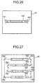
- the seventh embodiment provides an optical waveguide provided with micro mirrors in its inside in order to emit/receive propagated light upward/downward from/by the substrate's surface, wherein the micro mirrors are adjusted so that quantity of reflected light becomes constant.
- each micro mirror is constructed such that an aluminum film 822 is provided only on an inclined surface of the light incident side of a salient 15.
- light propagated through the optical waveguide 14 is absorbed or scattered being affected by material properties, homogenization, interface shapes, and the like of component members such as the micro mirrors.
- the intensity of the propagated light attenuates as it is propagated through the inside of the optical waveguide.
- the micro mirrors are not formed inside the optical waveguide 14, the intensity decreases exponentially with respect to propagation distance in accordance with Lambert's law of absorption. Owing to existence of a micro mirror, an optical signal is partly deflected.
- the state of attenuation of an optical signal propagated inside the optical waveguide 14 is complex.
- an optical signal, which propagates in the direction 31 of the light incidence is successively attenuated as it arrives at the first, second, third, .... micro mirrors, decreasing in arrival quantity of light.
- quantity of light deflected by each micro mirror is successively decreased.
- an optical signal deflected by a micro mirror is emitted to the substrate 100 mounted with the photodetector 101 as shown in Fig. 9.
- quantity of light deflected by the micro mirror be more than the requirement of the sensitivity of the photodetector 101.
- quantity of light that is originally entered into the optical waveguide 14 should be sufficiently large, so that sufficient quantity of light is entered into the photodetector 101 placed above the micro mirror at which the optical signal arrives in the most largely attenuated condition.
- quantity of reflected light is adjusted to be constant depending on attenuance of light arriving at each micro mirror.
- a micro mirror close to the incident point of the light is formed smaller, and a micro mirror is formed larger as it is more distant from the incident point.
- the optical waveguide for which sizes of the micro mirrors are adjusted as described it is possible to make the quantity of light that originally enters into the optical waveguide 14 smaller, while making the quantity of reflected light at each micro mirror is made to be more than the requirement of the sensitivity of the photodetector.
- application of this arrangement to the optical multi-chip module as shown in Fig. 19 can reduce power consumption.
- the height of the mirrors is favorably 5 - 20 % of the height of the optical waveguide 14.
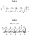
- the geometrically-progressive area change of the micro mirrors can be realized by making the salients 15 wider than the optical waveguide 14 as shown in Fig. 31, and by changing only the areas of the parts of the aluminum films 822 as reflecting films.
- the geometrically-progressive area change of the micro mirrors can be realized by changing the widths of the salients 15 as shown in Fig. 28, so as to adjust the areas of the reflecting films.
- This arrangement is favorable, since attenuation of an optical signal does not exist at the required salients 15, thus reducing the loss at the micro mirror portions.
- the micro mirrors are contained in the inside of the optical waveguide 14. Taking the margin of lithography into consideration, it is preferable that the end portion of the core is distant from the end portion of the mirror by more than or equal to 2 ⁇ m.
- the length of the salient 15 to form the micro mirror is 5 - 200 ⁇ m from the margin of lithography, seen in the direction of the propagation of an optical signal.
- geometrically-progressively changing areas of the micro mirrors can be realized by changing the heights of the mirrors geometrically, maintaining the width of the mirrors constant.
- the length of the reflecting films such as aluminum films 822 is 2 - 20 ⁇ m in the direction of the propagation of an optical signal. Too long aluminum film 822 acts as metal cladding, and as a result, invites excessive loss, while too short aluminum film makes lithography difficult.
- the size of the optical waveguide 14 is suitably 10 - 50 ⁇ m in width, and 5 - 20 ⁇ m in height.
- the optical waveguide 14 of too large size makes it impossible to obtain uniform intensity of the guided wave, since propagation modes increase too much.
- organic material for example polyimide, may be used as the material of the optical waveguide 14.
- constant quantity of reflected light means substantial constancy. Namely, it is sufficient if the quantity of reflected light is constant to such a degree that, when an optical signal kicked up by each micro mirror enters into the photodetector 101 mounted above the mirror, the optical signal does not become less than the detection sensitivity for any photodetector 101, and at the same time, the quantity of light originally entered into the optical waveguide 14 is not excessive.
- the shape of the inclined surface of the salient constituting the micro mirror may be any of flat, concave and convex surfaces. By selecting the shape of the flat, concave or convex surface depending on an object, it is possible to additionally produce an effect of converging or diffusing.
- the angle of the inclined surface of the salient 15 constituting the micro mirror may be any within the range of 0 - 90°.
- Figs. 28 - 31 show the constructions in which light is deflected upward.
- direction of deflection may be any of upward, downward and laterally directions. That direction can be decided taking the mounting position, mounting direction, etc. of the photodetector into consideration.
- the upper surface of the lower clad formed by this method becomes flat.
- the manufacturing method of the optical waveguide 14 having the micro mirrors such as shown in Fig. 30 will be described in more detail.
- the optical waveguide 14 of the seventh embodiment it is possible to suppress decrease of kicked-up quantity of light by making a mirror smaller at a position closer to the incident point, and larger at a more distant position. Further, by making the sizes of the mirrors larger than corresponding decrease of quantity of propagated light, it is also possible to increase kicked-up quantity of light by certain quantity, with ease. Accordingly, it is possible to kick up more quantity of light than the threshold of the photodetector 101, and thus, it is possible to increase the number of stages in which micro mirrors can be arranged in the optical waveguide 14.
- the present invention can provide a manufacturing method that can easily fabricate an optical waveguide provided with micro mirrors inside it, for receiving and emitting propagated light upward from the substrate.
- an optical waveguide substrate mounts substrates formed with electric circuits and photodetectors, it is possible to efficiently and compactly arrange lines for supplying power to the electric circuits, etc. by arranging them on the optical waveguide substrate.
- the manufacturing method of an optical waveguide provided with micro mirrors according to the present invention is advantageous to efficiently manufacturing an optical waveguide provided with micro mirrors.
- the optical waveguide provided with micro mirrors according to the present invention is advantageous as an optical waveguide propagating an optical signal in an optical information processing apparatus.
- the optical information processing apparatus according to the present invention can process information by means of an optical signal, and accordingly, it is advantageous as an information processing apparatus of a high processing speed
Landscapes
- Physics & Mathematics (AREA)
- General Physics & Mathematics (AREA)
- Optics & Photonics (AREA)
- Engineering & Computer Science (AREA)
- Microelectronics & Electronic Packaging (AREA)
- Optical Integrated Circuits (AREA)
Applications Claiming Priority (7)
| Application Number | Priority Date | Filing Date | Title |
|---|---|---|---|
| JP26900197 | 1997-10-01 | ||
| JP26900197 | 1997-10-01 | ||
| JP26900297 | 1997-10-01 | ||
| JP26900297 | 1997-10-01 | ||
| JP1612298 | 1998-01-28 | ||
| JP1612298 | 1998-01-28 | ||
| PCT/JP1998/004433 WO1999017143A1 (en) | 1997-10-01 | 1998-10-01 | Optical waveguide with micromirror, its manufacturing method, and optical information processor |
Publications (3)
| Publication Number | Publication Date |
|---|---|
| EP1020749A1 true EP1020749A1 (de) | 2000-07-19 |
| EP1020749A4 EP1020749A4 (de) | 2001-04-11 |
| EP1020749B1 EP1020749B1 (de) | 2009-02-18 |
Family
ID=27281259
Family Applications (1)
| Application Number | Title | Priority Date | Filing Date |
|---|---|---|---|
| EP98945563A Expired - Lifetime EP1020749B1 (de) | 1997-10-01 | 1998-10-01 | Optischer wellenleiter mit mikrospiegel, sein herstellungsverfahren, und optischer signalprozessor |
Country Status (6)
| Country | Link |
|---|---|
| EP (1) | EP1020749B1 (de) |
| KR (1) | KR100460388B1 (de) |
| CN (1) | CN1208650C (de) |
| AU (1) | AU9281498A (de) |
| DE (1) | DE69840575D1 (de) |
| WO (1) | WO1999017143A1 (de) |
Cited By (1)
| Publication number | Priority date | Publication date | Assignee | Title |
|---|---|---|---|---|
| US7425286B2 (en) | 2002-03-25 | 2008-09-16 | Canon Kabushiki Kaisha | Method of making optical waveguide apparatus |
Families Citing this family (7)
| Publication number | Priority date | Publication date | Assignee | Title |
|---|---|---|---|---|
| JP2003050329A (ja) * | 2001-08-06 | 2003-02-21 | Toppan Printing Co Ltd | 光・電気配線基板及びその製造方法並びに実装基板 |
| US7039263B2 (en) * | 2002-09-24 | 2006-05-02 | Intel Corporation | Electrooptic assembly |
| JP2007114374A (ja) * | 2005-10-19 | 2007-05-10 | Hitachi Cable Ltd | 光導波路素子及び多連光導波路素子 |
| CN104199262B (zh) * | 2014-08-08 | 2018-04-27 | 珠海赛纳打印科技股份有限公司 | 挡纸机构、进纸部、图像形成设备及进纸方法 |
| CN105974744A (zh) * | 2016-05-25 | 2016-09-28 | 淮阴工学院 | 一种基于聚甲基苯基硅烷/聚甲基丙烯酸苄酯共聚物光波导的微反射镜制作方法 |
| CN111326533B (zh) * | 2018-12-14 | 2023-01-13 | 上海新微技术研发中心有限公司 | 一种波导集成型光电探测器及其制作方法 |
| CN110673261B (zh) | 2019-09-06 | 2021-01-22 | 上海大学 | 基于紫外灰阶光刻制备光波导球形凹面镜的方法 |
Family Cites Families (5)
| Publication number | Priority date | Publication date | Assignee | Title |
|---|---|---|---|---|
| JPS59101217U (ja) * | 1982-12-27 | 1984-07-07 | 日本板硝子株式会社 | 光分配ダクト |
| JPH02108023A (ja) * | 1988-10-17 | 1990-04-19 | Semiconductor Energy Lab Co Ltd | 液晶電気光学装置 |
| US5170448A (en) * | 1992-01-06 | 1992-12-08 | Motorola, Inc. | Optical waveguide apparatus and method for partially collecting light |
| JP2986140B2 (ja) * | 1993-12-24 | 1999-12-06 | 日本電気株式会社 | マルチチップモジュール |
| JP3064224B2 (ja) * | 1995-11-27 | 2000-07-12 | 松下電工株式会社 | 照明装置 |
-
1998
- 1998-10-01 AU AU92814/98A patent/AU9281498A/en not_active Abandoned
- 1998-10-01 EP EP98945563A patent/EP1020749B1/de not_active Expired - Lifetime
- 1998-10-01 WO PCT/JP1998/004433 patent/WO1999017143A1/ja not_active Ceased
- 1998-10-01 CN CNB988096781A patent/CN1208650C/zh not_active Expired - Fee Related
- 1998-10-01 DE DE69840575T patent/DE69840575D1/de not_active Expired - Lifetime
- 1998-10-01 KR KR10-2000-7003091A patent/KR100460388B1/ko not_active Expired - Fee Related
Cited By (1)
| Publication number | Priority date | Publication date | Assignee | Title |
|---|---|---|---|---|
| US7425286B2 (en) | 2002-03-25 | 2008-09-16 | Canon Kabushiki Kaisha | Method of making optical waveguide apparatus |
Also Published As
| Publication number | Publication date |
|---|---|
| CN1272182A (zh) | 2000-11-01 |
| WO1999017143A1 (en) | 1999-04-08 |
| CN1208650C (zh) | 2005-06-29 |
| AU9281498A (en) | 1999-04-23 |
| DE69840575D1 (de) | 2009-04-02 |
| KR20010030678A (ko) | 2001-04-16 |
| EP1020749B1 (de) | 2009-02-18 |
| EP1020749A4 (de) | 2001-04-11 |
| KR100460388B1 (ko) | 2004-12-08 |
Similar Documents
| Publication | Publication Date | Title |
|---|---|---|
| US7079741B2 (en) | Optical interconnection circuit board and manufacturing method thereof | |
| US6611635B1 (en) | Opto-electronic substrates with electrical and optical interconnections and methods for making | |
| JP4457545B2 (ja) | 光・電気配線基板、実装基板及び光電気配線基板の製造方法 | |
| US6845184B1 (en) | Multi-layer opto-electronic substrates with electrical and optical interconnections and methods for making | |
| US6343171B1 (en) | Systems based on opto-electronic substrates with electrical and optical interconnections and methods for making | |
| CN110945976A (zh) | 基于带有聚合物波导的玻璃基板的光学互连模块 | |
| JP3257776B2 (ja) | 光モジュール実装構造 | |
| KR100463911B1 (ko) | 광정보처리장치 | |
| US7526153B2 (en) | Optical element device and two-dimensional optical waveguide device and optoelectronic circuit board using the same | |
| JP3570874B2 (ja) | 光接続構造 | |
| EP1020749A1 (de) | Optischer wellenleiter mit mikrospiegel, sein herstellungsverfahren, und optischer signalprozessor | |
| JP3652080B2 (ja) | 光接続構造 | |
| JP3285539B2 (ja) | 光モジュール実装構造 | |
| JPH1152198A (ja) | 光接続構造 | |
| JP2930178B2 (ja) | 導波路型光デバイスの受光構造 | |
| JP3920249B2 (ja) | 光導波路 | |
| JPWO1999017143A1 (ja) | マイクロミラーを備えた光導波路、その製造方法および光情報処理装置 | |
| JP4194515B2 (ja) | 二次元光導波装置、及びそれを用いた光電融合配線基板 | |
| JPH03238405A (ja) | 光送受信器一体化モジュール | |
| JP2001091773A (ja) | 光回路モジュール | |
| Ogunsola et al. | Polymer Pillars as Optical I/O for Gigascale Chips using Mirror-Terminated Waveguides | |
| CN121484639A (zh) | 封装结构及其制造方法 | |
| JPS62204208A (ja) | 光配線回路 | |
| JP2007123574A (ja) | 光クロック分配装置 |
Legal Events
| Date | Code | Title | Description |
|---|---|---|---|
| PUAI | Public reference made under article 153(3) epc to a published international application that has entered the european phase |
Free format text: ORIGINAL CODE: 0009012 |
|
| 17P | Request for examination filed |
Effective date: 20000429 |
|
| AK | Designated contracting states |
Kind code of ref document: A1 Designated state(s): DE FI FR GB NL SE |
|
| A4 | Supplementary search report drawn up and despatched |
Effective date: 20010228 |
|
| AK | Designated contracting states |
Kind code of ref document: A4 Designated state(s): DE FI FR GB NL SE |
|
| RIC1 | Information provided on ipc code assigned before grant |
Free format text: 7G 02B 6/12 A |
|
| 17Q | First examination report despatched |
Effective date: 20041028 |
|
| GRAP | Despatch of communication of intention to grant a patent |
Free format text: ORIGINAL CODE: EPIDOSNIGR1 |
|
| GRAS | Grant fee paid |
Free format text: ORIGINAL CODE: EPIDOSNIGR3 |
|
| GRAA | (expected) grant |
Free format text: ORIGINAL CODE: 0009210 |
|
| AK | Designated contracting states |
Kind code of ref document: B1 Designated state(s): DE FI FR GB NL SE |
|
| REG | Reference to a national code |
Ref country code: GB Ref legal event code: FG4D |
|
| REF | Corresponds to: |
Ref document number: 69840575 Country of ref document: DE Date of ref document: 20090402 Kind code of ref document: P |
|
| REG | Reference to a national code |
Ref country code: SE Ref legal event code: TRGR |
|
| PLBE | No opposition filed within time limit |
Free format text: ORIGINAL CODE: 0009261 |
|
| STAA | Information on the status of an ep patent application or granted ep patent |
Free format text: STATUS: NO OPPOSITION FILED WITHIN TIME LIMIT |
|
| 26N | No opposition filed |
Effective date: 20091119 |
|
| PGFP | Annual fee paid to national office [announced via postgrant information from national office to epo] |
Ref country code: SE Payment date: 20091007 Year of fee payment: 12 Ref country code: FI Payment date: 20091020 Year of fee payment: 12 |
|
| PGFP | Annual fee paid to national office [announced via postgrant information from national office to epo] |
Ref country code: NL Payment date: 20091020 Year of fee payment: 12 |
|
| PGFP | Annual fee paid to national office [announced via postgrant information from national office to epo] |
Ref country code: GB Payment date: 20091002 Year of fee payment: 12 |
|
| PGFP | Annual fee paid to national office [announced via postgrant information from national office to epo] |
Ref country code: DE Payment date: 20091204 Year of fee payment: 12 |
|
| REG | Reference to a national code |
Ref country code: NL Ref legal event code: V1 Effective date: 20110501 |
|
| GBPC | Gb: european patent ceased through non-payment of renewal fee |
Effective date: 20101001 |
|
| PG25 | Lapsed in a contracting state [announced via postgrant information from national office to epo] |
Ref country code: FR Free format text: LAPSE BECAUSE OF NON-PAYMENT OF DUE FEES Effective date: 20101102 |
|
| REG | Reference to a national code |
Ref country code: FR Ref legal event code: ST Effective date: 20110630 |
|
| REG | Reference to a national code |
Ref country code: DE Ref legal event code: R119 Ref document number: 69840575 Country of ref document: DE Effective date: 20110502 |
|
| PG25 | Lapsed in a contracting state [announced via postgrant information from national office to epo] |
Ref country code: FI Free format text: LAPSE BECAUSE OF NON-PAYMENT OF DUE FEES Effective date: 20101001 Ref country code: NL Free format text: LAPSE BECAUSE OF NON-PAYMENT OF DUE FEES Effective date: 20110501 Ref country code: GB Free format text: LAPSE BECAUSE OF NON-PAYMENT OF DUE FEES Effective date: 20101001 |
|
| PG25 | Lapsed in a contracting state [announced via postgrant information from national office to epo] |
Ref country code: SE Free format text: LAPSE BECAUSE OF NON-PAYMENT OF DUE FEES Effective date: 20101002 |
|
| PGFP | Annual fee paid to national office [announced via postgrant information from national office to epo] |
Ref country code: FR Payment date: 20090908 Year of fee payment: 12 |
|
| PG25 | Lapsed in a contracting state [announced via postgrant information from national office to epo] |
Ref country code: DE Free format text: LAPSE BECAUSE OF NON-PAYMENT OF DUE FEES Effective date: 20110502 |