EP1022749B1 - Diviseur de tension capacitif électrostatique - Google Patents
Diviseur de tension capacitif électrostatique Download PDFInfo
- Publication number
- EP1022749B1 EP1022749B1 EP20000101081 EP00101081A EP1022749B1 EP 1022749 B1 EP1022749 B1 EP 1022749B1 EP 20000101081 EP20000101081 EP 20000101081 EP 00101081 A EP00101081 A EP 00101081A EP 1022749 B1 EP1022749 B1 EP 1022749B1
- Authority
- EP
- European Patent Office
- Prior art keywords
- layer
- conductor
- metallic
- metallic layer
- voltage transformer
- Prior art date
- Legal status (The legal status is an assumption and is not a legal conclusion. Google has not performed a legal analysis and makes no representation as to the accuracy of the status listed.)
- Expired - Lifetime
Links
- 239000010410 layer Substances 0.000 claims description 124
- 239000004020 conductor Substances 0.000 claims description 75
- 239000011241 protective layer Substances 0.000 claims description 6
- 230000001939 inductive effect Effects 0.000 description 13
- 238000004804 winding Methods 0.000 description 8
- 239000000463 material Substances 0.000 description 4
- 239000003990 capacitor Substances 0.000 description 2
- 238000001514 detection method Methods 0.000 description 2
- 230000005684 electric field Effects 0.000 description 2
- 230000007935 neutral effect Effects 0.000 description 2
- 238000010248 power generation Methods 0.000 description 2
- 239000004593 Epoxy Substances 0.000 description 1
- XEEYBQQBJWHFJM-UHFFFAOYSA-N Iron Chemical group [Fe] XEEYBQQBJWHFJM-UHFFFAOYSA-N 0.000 description 1
- 238000010586 diagram Methods 0.000 description 1
- 230000008030 elimination Effects 0.000 description 1
- 238000003379 elimination reaction Methods 0.000 description 1
- 239000011888 foil Substances 0.000 description 1
- 238000009434 installation Methods 0.000 description 1
- 239000012212 insulator Substances 0.000 description 1
- 238000004519 manufacturing process Methods 0.000 description 1
- 238000012986 modification Methods 0.000 description 1
- 230000004048 modification Effects 0.000 description 1
- 230000000149 penetrating effect Effects 0.000 description 1
- 238000007789 sealing Methods 0.000 description 1
- 239000004065 semiconductor Substances 0.000 description 1
- 239000000725 suspension Substances 0.000 description 1
- 239000012815 thermoplastic material Substances 0.000 description 1
- 229920001187 thermosetting polymer Polymers 0.000 description 1
Images


Classifications
-
- H—ELECTRICITY
- H01—ELECTRIC ELEMENTS
- H01B—CABLES; CONDUCTORS; INSULATORS; SELECTION OF MATERIALS FOR THEIR CONDUCTIVE, INSULATING OR DIELECTRIC PROPERTIES
- H01B17/00—Insulators or insulating bodies characterised by their form
- H01B17/005—Insulators structurally associated with built-in electrical equipment
Definitions
- the present invention relates to an electrostatic capacitive divided-voltage transformer utilizing a power cable or insulating bus bar and applicable to a voltage detector.
- a voltage transformer includes an inductive VT having a transformer structure and an electrostatic capacitive VT having serially-connected capacitors.
- a usage division between the inductive VT and the electrostatic capacitive VT will be made generally in the following way according to a line voltage (system voltage).
- the inductive VT has been used up to the line voltage of 36 kV and the electrostatic capacitive divided-voltage VT has been used for a high voltage application equal to or higher than 72.5 kV.
- the inductive VT has been used up to 245 kV and the electrostatic capacitive divided-voltage VT has been used for a voltage application higher than 300 kV.
- a boundary between the usage division between the inductive VT and capacitive VT is not strictly determined but is determined for an economical reason such that which one of the two type transformers is cheaper under the same specification.
- the electrostatic capacitive divided-voltage transformer is more economically advantageous than the inductive VT.
- Japanese Patent Application First Publication No. Heisei 8-51719 published on February 20, 1996 (corresponds to a United States Patent No. 5,493,072 issued on February 20, 1996) exemplifies a previously proposed series-connected capacitive graded high-voltage cable terminator and suspension insulator.
- Japanese Patent Application First Publication No. Heisei 10-79205 published on March 24, 1998 exemplifies a previously proposed power cable.
- a secondary load of the VT (voltage transformer) is extremely lowered.
- the VT has a load which conventionally indicates 200 VA but which is recently reduced to 30 VA.
- the VT equal to or higher than the voltage 72.5 kV has the load which indicates conventionally 500 VA but which recently indicates 50VA. In the future, a reduction rate of the secondary load will be increased.
- the VT may possibly be the capacitive VT.
- a limit of manufacturing the capacitive VT can further be expanded.
- an electrostatic capacitive divided-voltage transformer according to claim 1.
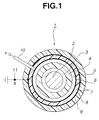
- Fig. 1 shows a cross sectional view of a first preferred embodiment of an electrostatic capacitance voltage division type voltage transformer (also called, an electrostatic capacitive divided-voltage transformer abbreviated as a CVT) utilizing a power cable or in an insulating bus bar.
- an electrostatic capacitance voltage division type voltage transformer also called, an electrostatic capacitive divided-voltage transformer abbreviated as a CVT
- the whole CVT denoted by a reference numeral of 1 includes: an inner conductor 2 having a circular shape in cross section; an inner semiconductive layer 3 to make relaxation of electric field and potential around the conductor 2; a main insulative layer 4; and an outer semiconductor layer 5 to make relaxation of electric field and potential.
- These layers 3, 4, and 5 enclosing the conductor 2 in this order are in the form of either a power cable or an insulating bus bar.
- the CVT 1 further includes a metallic layer 6 for an electrostatic capacitance voltage division purpose (hereinafter called, a first metallic layer); an auxiliary insulative layer 7; a ground metallic layer 8 (hereinafter also called, a second metallic layer); and a protective layer 9 which serves as an outmost layer of the CVT 1 and which is arranged on the second metallic layer 8 according to its necessity.
- a voltage division tap T is led by means of an insulated wire 10 from the voltage division metallic layer 6 and a grounded tap E is led from the second metallic layer 8 by means of a conductive wire 11.
- the protective layer 9 is installed with a mechanical stress elimination, an anti-weather characteristic, and a thermal dissipation taken into consideration.
- Material and thickness of the auxiliary insulative layer 7 are selected so that a capacitance C 2 across the insulative layer 7 is derived with a ratio thereof to a capacitance C 1 across the main insulative layer 4 taken into consideration.
- the voltage division tap T is led via the insulated wire 10 to any one of the cable connection points and from the ground (second) metallic layer 8, the conductive wire 11 is used to lead out the ground tap E.
- the ratio of C 1 /C 2 is constant although each capacitance changes with the length of the power cable or the insulating bus bar. Hence, a minimum required electrostatic capacitance for each voltage is determined. If the cable size is determined, a shortest length of the cable is calculated so that a free application above the length of the cable can be made.
- Fig. 2 shows an application example of the CVT 1 shown in Fig. 1 to a three-phase CVT.
- Fig. 2 three of the same CVTs (1 R , 1 Y , 1 B ) as shown in Fig. 1 are star-connected with the grounded tap E as a neutral point.
- three-phase taps T R , T Y , and T B are led out and are connected to a three-phase low-voltage VT box 22 via corresponding low-voltage insulated cables (or low-voltage shielded wire) 21.
- Each low-voltage insulating cable 21 is further connected to a corresponding primary winding 26 of a three-phase low-voltage VT 25 using a five-leg iron core 24 via its corresponding choke coil 23.
- a connection form of each primary winding 26, each secondary winding 27, and each third winding 28 is a star, a star, and an open delta form and star neutral points in the star connection forms are grounded.
- the low-voltage VT box 22 may be attached onto a position a slightly far away from the CVT 1, for example, a position outside of a tank of GIS (Gas Insulated Switchgear). Output ends of each secondary winding 27 and each third winding 28 of the low-voltage VT 25 from a terminal box 29 is supplied to corresponding input ends of a digital meter or a digital relay (not shown).
- GIS Gas Insulated Switchgear
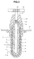
- Fig. 3 shows an example of an application of the electrostatic capacitive divided-voltage transformer shown in Fig. 1 to a GIS device.
- the CVT 1 has one end 2 2 of the conductor 2 sealingly enclosed with each layer member, i.e., the inner semiconductive layer 3, the main insulative layer 4, the outer semiconductive layer 5, the first metallic layer 6, the auxiliary metallic layer 7, and the second grounded metallic layer 8.
- each layer member i.e., the inner semiconductive layer 3, the main insulative layer 4, the outer semiconductive layer 5, the first metallic layer 6, the auxiliary metallic layer 7, and the second grounded metallic layer 8.
- the CVT 1 is covered with the protective layer 9 with a conductor 2 2 projected from the other end of the conductor 2.
- a bushing 32 is provided with a conductor 2 1 used to connect a device vessel 31 such as GIS and a connector 34 is installed to connect the CVT 1 to an inner conductor 33 of the device vessel 31.
- the bushing conductor 2 1 is connected to the connector 34.
- a connector 2 3 is installed so as to enable a connection between the bushing-sided conductor 2 1 and the CVT-sided conductor 2 2 .
- the CVT-sided conductor 2 2 can be connected to the inner conductor 33 of the GIS via the bushing-sided conductor 21.
- the divided voltage tap T and the grounded tap E are led out from the CVT 1 and projected from the outside of the GIS. It is noted that a hermetic sealing is provided between the bushing 32 and the device vessel 31 and between the bushing 32 and CVT 1 and CVT 1 should tightly be fitted into the bushing 32.
- Fig. 4 shows another example of the application of the electrostatic capacitive divided-voltage transformer (CVT) shown in Fig. 1.
- CVT electrostatic capacitive divided-voltage transformer
- a power cable 1 1 connecting to a device 41 or an insulating bus bar 1 2 connected between the devices 41 and 41 is formed of the CVT in the same manner as shown in Fig. 1.
- Cable connectors 42 are attached to the corresponding devices 41 and 41.
- the tap T and the grounded tap E (not shown) are drawn out from one of the connectors 42.
- the power cable 1 1 functions as both of the cable and the CVT and the insulating bus bar 1 2 functions as the bus bar and the CVT.
- the tap T and the grounded tap E are always a pair and either of the respective side connectors is drawn out as the tap T and the grounded tap E.
- each insulative material of the main and auxiliary insulative layers 4 and 7 is made of a thermoplastic material, a flexible CVT as the power cable can be achieved.
- each insulative material of the main and auxiliary insulative layers 4 and 7 is made of a thermosetting material, the CVT having a high rigidity and a large mechanical strength such as an epoxy molded product can be achieved.
- Figs. 5 and 6 show second and third preferred embodiments of the electrostatic capacitive divided-voltage transformer.
- the CVT 1 in each of the second and third preferred embodiments of the electrostatic capacitive divided-voltage transformer includes: the substantially cylindrical inner conductor 2 which is a bus bar used to connect the device to GIS and which is capable of carrying the current having the same values as in the case of Fig. 1; the inner semiconductive layer 3; the main insulative layer 4; the outer semiconductive layer 5; the first metallic layer 6; the auxiliary insulative layer 7; and the cylindrically grounded metallic layer 8, sequentially on the inner conductor in the same manner shown in Fig. 1.
- Another auxiliary insulative layer 61, another first metallic layer 62, another semiconductive layer 63, another outer main insulative layer 64, another semiconductive layer 65, and another outer conductor 66 made of a cylindrical foil are arranged on the second grounded metallic layer in this sequence. Furthermore, another semiconductive layer 67, another outer main insulative layer 68, another semiconductive layer 69, another first metallic layer 70, another auxiliary insulative layer 71, another second grounded metallic layer 72, and another protective layer 73 are arranged in this sequence.
- the inner conductor 2 is connected with the outer conductor 66 via an insulated wire 74 to make the outer conductor 66 the same potential as the inner conductor.
- the first metallic layers 6, 62, 70 are connected together via another insulated wire 75 to produce the tap T.
- the second grounded metallic layers 8 and 72 are connected via the insulated wire 76 to produce a tap E.
- the electrostatic capacitance between the inner conductor 2 and the first metallic layer 6 is C 1
- the electrostatic capacitance between the first metallic layer 6 and the second grounded metallic layer 8 is C 2
- an electrostatic capacitance between the second grounded metallic layer 8 and the other first metallic layer 62 is C 2 '
- an electrostatic capacitance between the other first metallic layer 62 and the outer conductor 66 is C 1 '
- an electrostatic capacitance between the outer conductor 66 and the other metallic layer 70 is C 1 "
- an electrostatic capacitance between the first metallic layer 70 and the other second metallic layer 72 is C 2 ''.
- An electrostatic capacitance between the tap T and the grounded tap E is C 2 + C 2 ' + C 2 ".
- a large CVT having a large electrostatic capacitance can be achieved.
- the bushing 32 shown in Fig. 6 includes the bushing-sided conductor 2 1 in the same manner as shown in Fig. 3.
- the bushing 32 is attached onto the device vessel 31.
- a conductor 2 3 is installed on a lower end of the bushing-sided conductor 2 1 .
- a large current can be supplied to a load through the inner conductor 2 of the CVT 1.
- the divided voltage can be outputted from the tap T.
- the CVT having the relatively large electrostatic capacity and having the bus bar used to connect the device to the GIS can be achieved. If a low-voltage penetrating type current transformer or a low-voltage dividing type current transformer is arranged on an outside of this bus bar, the CVT shown in Figs. 5 or 6 serves as a bus bar functioning as a voltage-and-current transformer for an integrated instrument purpose.
- the CVT 1 in each of the second and third embodiments shown in Figs. 5 or 6 includes the single outer conductor.
- a plurality of outer conductors may concentrically be installed, the grounded metallic layer may be interposed between the respective outer conductors.
- the semiconductive layer, the main insulative layer, the semiconductive layer, the first metallic layer, and the auxiliary insulative layer may be installed between the respectively corresponding ones of the outer conductors and of the second grounded metallic layers.
- the inner conductor and the plurality of outer conductors may be connected via an electric wire 74.
- the metallic layer and each grounded metallic layer are connected to the electric wires 75 and 76 to achieve the CVT having the further large electrostatic capacity.
Landscapes
- Transformers For Measuring Instruments (AREA)
- Measuring Instrument Details And Bridges, And Automatic Balancing Devices (AREA)
- Gas-Insulated Switchgears (AREA)
Claims (9)
- Transformateur diviseur de tension capacitif électrostatique, comprenant :un conducteur (2) ;une couche semi-conductrice intérieure (3) ;une couche isolante principale (4) ; etune couche semi-conductrice extérieure (5) ;caractérisé en ce que le conducteur (2) est enfermé avec la couche semi-conductrice intérieure, la couche isolante principale, et la couche semi-conductrice extérieure dans cette séquence, et le transformateur diviseur de tension capacitif électrostatique comprend en outre :une première couche métallique (6), la première couche métallique enfermant la couche semi-conductrice extérieure ; une couche isolante auxiliaire (7) agencée sur la première couche métallique ; une seconde couche métallique (8) agencée sur la couche isolante auxiliaire, une tension divisée à partir d'une tension globale entre le conducteur et la seconde couche métallique étant en mesure de passer entre la première couche métallique et la seconde couche métallique ; et une première prise de prélèvement (T) menée hors de la première couche métallique via un fil isolant (10), et une seconde prise de prélèvement (E) menée hors de la seconde couche métallique, la seconde prise de prélèvement étant mise à la terre.
- Transformateur diviseur de tension capacitif électrostatique selon la revendication 1, caractérisé en ce que le transformateur diviseur de tension capacitif électrostatique inclut en outre une couche protectrice (9) qui enferme la seconde couche métallique (8).
- Transformateur diviseur de tension capacitive électrostatique selon la revendication 2, caractérisé en ce que le conducteur (2) inclut : une partie conductrice (22), dont une extrémité est scellée avec la couche semi-conductrice intérieure (3), la couche isolante principale (4), la couche semi-conductrice extérieure (5), la première couche métallique (6), la couche isolante auxiliaire (7), la seconde couche métallique (8), et la couche protectrice (9), et dont l'autre extrémité est connectée à un connecteur (23), ledit connecteur (23) étant connecté à un autre conducteur (21) susceptible d'être connecté à un conducteur de circuit (33) d'un commutateur (31) isolé par un gaz.
- Transformateur diviseur de tension capacitif électrostatique selon la revendication 3, caractérisé en ce que le transformateur diviseur de tension capacitif électrostatique inclut en outre une douille (32) qui comporte à l'intérieur l'autre conducteur (21), et le connecteur (23) est connecté de façon déconnectable entre l'autre conducteur (21) et la partie conductrice (22).
- Transformateur diviseur de tension capacitif électrostatique selon la revendication 1, caractérisé en ce que le conducteur (2), la couche semi-conductrice intérieure (3), la couche isolante principale (4), et la couche semi-conductrice extérieure (5) constituent un câble de puissance.
- Transformateur diviseur de tension capacitif électrostatique selon la revendication 1, caractérisé en ce que le conducteur (2), la couche semi-conductrice intérieure (3), la couche isolante principale (4), et la couche semi-conductrice extérieure (5) constituent une barre de bus isolante.
- Transformateur diviseur de tension capacitif électrostatique selon la revendication 1, caractérisé en ce que le conducteur (2) est un conducteur intérieur de forme cylindrique qui constitue une barre de bus, un conducteur extérieur (66) ayant le même potentiel que le conducteur intérieur est agencé concentriquement sur le conducteur intérieur, la seconde couche métallique (8) est agencée concentriquement entre le conducteur intérieur et le conducteur extérieur, et une autre seconde couche métallique (72) est agencée concentriquement sur le conducteur extérieur, et la première couche métallique inclut une pluralité de premières couches métalliques (6, 62, 70), chacune des premières couches métalliques étant agencée concentriquement entre le conducteur intérieur et la seconde couche métallique, entre la seconde couche métallique et le conducteur extérieur, et entre le conducteur extérieur et l'autre seconde couche métallique, les conducteurs intérieur et extérieur étant connectés électriquement, et la seconde couche métallique et l'autre seconde couche métallique étant connectées ensemble.
- Transformateur diviseur de tension capacitif électrostatique selon la revendication 1, caractérisé en ce que le conducteur (2) est un conducteur intérieur de forme cylindrique qui constitue une barre de bus, une pluralité de conducteurs extérieurs (66), chacun des conducteurs extérieurs ayant le même potentiel que le conducteur intérieur, son agencés concentriquement entre le conducteur intérieur et les conducteurs extérieurs respectifs, et une autre seconde couche métallique (72) est agencée concentriquement sur l'un des conducteurs extérieurs placé le plus à l'extérieur, et la première couche métallique inclut une pluralité de premières couches métalliques (6, 62, 70), chacune des premières couches métalliques étant agencée concentriquement entre le conducteur intérieur et les secondes couches métalliques respectives, entre les secondes couches métalliques respectives et les conducteurs extérieurs respectifs, et entre le conducteur extérieur le plus extérieur et l'une des secondes couches métalliques située le plus à l'extérieur, les conducteurs intérieurs et extérieurs étant connectés électriquement, les secondes couches métalliques étant connectées ensemble.
- Transformateur diviseur de tension capacitif électrostatique selon la revendication 7, caractérisé en ce que chacune des secondes couches métalliques est mise à la terre via une prise de prélèvement (E) mise à la terre, et si la capacité électrostatique entre le conducteur intérieur (2) et la première couche métallique (6) est C1, la capacité électrostatique entre la seconde couche métallique (8) mise à la terre et la première couche métallique (62) est C2', et la capacité électrostatique entre la première couche métallique (62) et le conducteur extérieur (66) est C1', la capacité électrostatique entre la première couche métallique (66) et la première couche métallique (70) est C1", la capacité électrostatique entre la première couche métallique (70) et la seconde couche métallique (72) est C2", la capacité électrostatique entre le conducteur intérieur (2) et la prise de prélèvement (T) est exprimée sous la forme C1 + C1' + C1", la capacité électrostatique entre la prise de prélèvement (T) et la prise de prélèvement (E) mise à la terre est exprimée sous la forme C2 + C2' + C2", et C1 = C1' = C1" et C2 = C2' = C2".
Applications Claiming Priority (4)
| Application Number | Priority Date | Filing Date | Title |
|---|---|---|---|
| JP1376099 | 1999-01-22 | ||
| JP1376099 | 1999-01-22 | ||
| JP11302117A JP2000277363A (ja) | 1999-01-22 | 1999-10-25 | 静電容量分圧形電圧変成器 |
| JP30211799 | 1999-10-25 |
Publications (2)
| Publication Number | Publication Date |
|---|---|
| EP1022749A1 EP1022749A1 (fr) | 2000-07-26 |
| EP1022749B1 true EP1022749B1 (fr) | 2006-09-06 |
Family
ID=26349604
Family Applications (1)
| Application Number | Title | Priority Date | Filing Date |
|---|---|---|---|
| EP20000101081 Expired - Lifetime EP1022749B1 (fr) | 1999-01-22 | 2000-01-20 | Diviseur de tension capacitif électrostatique |
Country Status (3)
| Country | Link |
|---|---|
| EP (1) | EP1022749B1 (fr) |
| JP (1) | JP2000277363A (fr) |
| DE (1) | DE60030496T2 (fr) |
Families Citing this family (6)
| Publication number | Priority date | Publication date | Assignee | Title |
|---|---|---|---|---|
| WO2012130816A1 (fr) * | 2011-03-25 | 2012-10-04 | Eandis | Systèmes de mesure de haute tension |
| CN102928639B (zh) * | 2011-08-07 | 2016-03-02 | 江苏思源赫兹互感器有限公司 | 电子式电容分压器 |
| CN102709048B (zh) * | 2011-09-09 | 2013-09-11 | 上海良治电器技术有限公司 | 一种用于x光机高压线圈的绕制新工艺 |
| FR3025029B1 (fr) * | 2014-08-21 | 2016-08-05 | Nexans | Dispositif de mesure sans contact d'une tension electrique dans un cable de reseau electrique moyenne ou haute tension |
| CN107808711A (zh) * | 2017-11-13 | 2018-03-16 | 国网湖南省电力有限公司 | 一种变压器综合试验专用测试电缆 |
| CN116298706A (zh) * | 2022-09-08 | 2023-06-23 | 中电新源(廊坊)电气集团有限公司 | 低压三相三角形接线系统及交流低压系统的绝缘监测方法 |
Family Cites Families (2)
| Publication number | Priority date | Publication date | Assignee | Title |
|---|---|---|---|---|
| US4466047A (en) * | 1981-08-06 | 1984-08-14 | Avocat Jean P | Capacitor for medium-range voltage capacitive dividers |
| DE3917862A1 (de) * | 1989-06-01 | 1990-12-06 | Asea Brown Boveri | Anordnung zur spannungsversorgung einer anzeigevorrichtung fuer die anzeige einer anliegenden netzspannung bei einer mittelspannungs-schaltanlage |
-
1999
- 1999-10-25 JP JP11302117A patent/JP2000277363A/ja active Pending
-
2000
- 2000-01-20 DE DE2000630496 patent/DE60030496T2/de not_active Expired - Fee Related
- 2000-01-20 EP EP20000101081 patent/EP1022749B1/fr not_active Expired - Lifetime
Also Published As
| Publication number | Publication date |
|---|---|
| DE60030496T2 (de) | 2007-02-01 |
| EP1022749A1 (fr) | 2000-07-26 |
| JP2000277363A (ja) | 2000-10-06 |
| DE60030496D1 (de) | 2006-10-19 |
Similar Documents
| Publication | Publication Date | Title |
|---|---|---|
| US7064267B2 (en) | Gas insulating apparatus and method for locating fault point thereof | |
| EA001725B1 (ru) | Мощный трансформатор или катушка индуктивности | |
| WO2021124035A1 (fr) | Dispositif de détection de tension installé en rattrapage pour réseaux d'alimentation | |
| US7027280B2 (en) | Gas insulating apparatus and method for locating fault point thereof | |
| CN111316113B (zh) | 分压器组件 | |
| EP1022749B1 (fr) | Diviseur de tension capacitif électrostatique | |
| EP1624311A1 (fr) | Transformateur de mesures combiné en courant et tension pour condensateur de traverse | |
| US3386059A (en) | Power line coupling device | |
| US4881147A (en) | Protection of sensitive electrical installations against the effects of lightning, and devices proposed for such arrangement | |
| CN217061742U (zh) | 带电压电流互感器的管母线仓 | |
| AU2020273556B2 (en) | High voltage transformer, method for producing a high voltage transformer and test system and test signal device comprising a high voltage transformer | |
| CA1067593A (fr) | Dispositif d'interface pour appareil haute tension a huile et a gaz | |
| KR102872860B1 (ko) | 전자식 전압 센서 | |
| US12476441B2 (en) | Arrangement of a current transformer core at an interface with a conical connector | |
| JPH0624991Y2 (ja) | ガス絶縁変成器 | |
| JPH09292435A (ja) | 耐電圧試験保護装置 | |
| US12424845B1 (en) | Systems and methods for creating a wire coil short circuit reducer | |
| JP3985409B2 (ja) | ガス絶縁電気設備用変流器 | |
| US20260094758A1 (en) | Transformer apparatus | |
| JP2008521231A (ja) | 絶縁変圧器 | |
| US20250370010A1 (en) | Low power instrument transformer (lpit) in conical connector | |
| CN100533613C (zh) | 一种用特殊电缆绕组制成的分裂变压器 | |
| US11626244B2 (en) | Assembly for connecting to a high-voltage grid | |
| CN111869025B (zh) | 具有测量互感器和过电压放电器的设备 | |
| JP3627959B2 (ja) | 計器用変圧変流器 |
Legal Events
| Date | Code | Title | Description |
|---|---|---|---|
| PUAI | Public reference made under article 153(3) epc to a published international application that has entered the european phase |
Free format text: ORIGINAL CODE: 0009012 |
|
| 17P | Request for examination filed |
Effective date: 20000120 |
|
| AK | Designated contracting states |
Kind code of ref document: A1 Designated state(s): CH DE FR LI |
|
| AX | Request for extension of the european patent |
Free format text: AL;LT;LV;MK;RO;SI |
|
| AKX | Designation fees paid |
Free format text: CH DE FR LI |
|
| 17Q | First examination report despatched |
Effective date: 20040524 |
|
| GRAP | Despatch of communication of intention to grant a patent |
Free format text: ORIGINAL CODE: EPIDOSNIGR1 |
|
| GRAS | Grant fee paid |
Free format text: ORIGINAL CODE: EPIDOSNIGR3 |
|
| GRAA | (expected) grant |
Free format text: ORIGINAL CODE: 0009210 |
|
| AK | Designated contracting states |
Kind code of ref document: B1 Designated state(s): CH DE FR LI |
|
| REG | Reference to a national code |
Ref country code: CH Ref legal event code: EP |
|
| REF | Corresponds to: |
Ref document number: 60030496 Country of ref document: DE Date of ref document: 20061019 Kind code of ref document: P |
|
| PGFP | Annual fee paid to national office [announced via postgrant information from national office to epo] |
Ref country code: CH Payment date: 20070112 Year of fee payment: 8 |
|
| ET | Fr: translation filed | ||
| PGFP | Annual fee paid to national office [announced via postgrant information from national office to epo] |
Ref country code: DE Payment date: 20070330 Year of fee payment: 8 |
|
| PLBE | No opposition filed within time limit |
Free format text: ORIGINAL CODE: 0009261 |
|
| STAA | Information on the status of an ep patent application or granted ep patent |
Free format text: STATUS: NO OPPOSITION FILED WITHIN TIME LIMIT |
|
| 26N | No opposition filed |
Effective date: 20070607 |
|
| PGFP | Annual fee paid to national office [announced via postgrant information from national office to epo] |
Ref country code: FR Payment date: 20070111 Year of fee payment: 8 |
|
| REG | Reference to a national code |
Ref country code: CH Ref legal event code: PL |
|
| PG25 | Lapsed in a contracting state [announced via postgrant information from national office to epo] |
Ref country code: LI Free format text: LAPSE BECAUSE OF NON-PAYMENT OF DUE FEES Effective date: 20080131 Ref country code: DE Free format text: LAPSE BECAUSE OF NON-PAYMENT OF DUE FEES Effective date: 20080801 Ref country code: CH Free format text: LAPSE BECAUSE OF NON-PAYMENT OF DUE FEES Effective date: 20080131 |
|
| REG | Reference to a national code |
Ref country code: FR Ref legal event code: ST Effective date: 20081029 |
|
| PG25 | Lapsed in a contracting state [announced via postgrant information from national office to epo] |
Ref country code: FR Free format text: LAPSE BECAUSE OF NON-PAYMENT OF DUE FEES Effective date: 20080131 |