EP1024565A2 - Dispositif optique semi-conducteur et méthode de fabrication - Google Patents
Dispositif optique semi-conducteur et méthode de fabrication Download PDFInfo
- Publication number
- EP1024565A2 EP1024565A2 EP00101538A EP00101538A EP1024565A2 EP 1024565 A2 EP1024565 A2 EP 1024565A2 EP 00101538 A EP00101538 A EP 00101538A EP 00101538 A EP00101538 A EP 00101538A EP 1024565 A2 EP1024565 A2 EP 1024565A2
- Authority
- EP
- European Patent Office
- Prior art keywords
- layer
- fabricating
- optical device
- mesa structure
- mesa
- Prior art date
- Legal status (The legal status is an assumption and is not a legal conclusion. Google has not performed a legal analysis and makes no representation as to the accuracy of the status listed.)
- Withdrawn
Links
Images


Classifications
-
- H—ELECTRICITY
- H01—ELECTRIC ELEMENTS
- H01S—DEVICES USING THE PROCESS OF LIGHT AMPLIFICATION BY STIMULATED EMISSION OF RADIATION [LASER] TO AMPLIFY OR GENERATE LIGHT; DEVICES USING STIMULATED EMISSION OF ELECTROMAGNETIC RADIATION IN WAVE RANGES OTHER THAN OPTICAL
- H01S5/00—Semiconductor lasers
- H01S5/20—Structure or shape of the semiconductor body to guide the optical wave ; Confining structures perpendicular to the optical axis, e.g. index or gain guiding, stripe geometry, broad area lasers, gain tailoring, transverse or lateral reflectors, special cladding structures, MQW barrier reflection layers
- H01S5/22—Structure or shape of the semiconductor body to guide the optical wave ; Confining structures perpendicular to the optical axis, e.g. index or gain guiding, stripe geometry, broad area lasers, gain tailoring, transverse or lateral reflectors, special cladding structures, MQW barrier reflection layers having a ridge or stripe structure
- H01S5/227—Buried mesa structure ; Striped active layer
-
- H—ELECTRICITY
- H10—SEMICONDUCTOR DEVICES; ELECTRIC SOLID-STATE DEVICES NOT OTHERWISE PROVIDED FOR
- H10P—GENERIC PROCESSES OR APPARATUS FOR THE MANUFACTURE OR TREATMENT OF DEVICES COVERED BY CLASS H10
- H10P14/00—Formation of materials, e.g. in the shape of layers or pillars
- H10P14/20—Formation of materials, e.g. in the shape of layers or pillars of semiconductor materials
-
- H—ELECTRICITY
- H01—ELECTRIC ELEMENTS
- H01S—DEVICES USING THE PROCESS OF LIGHT AMPLIFICATION BY STIMULATED EMISSION OF RADIATION [LASER] TO AMPLIFY OR GENERATE LIGHT; DEVICES USING STIMULATED EMISSION OF ELECTROMAGNETIC RADIATION IN WAVE RANGES OTHER THAN OPTICAL
- H01S5/00—Semiconductor lasers
- H01S5/20—Structure or shape of the semiconductor body to guide the optical wave ; Confining structures perpendicular to the optical axis, e.g. index or gain guiding, stripe geometry, broad area lasers, gain tailoring, transverse or lateral reflectors, special cladding structures, MQW barrier reflection layers
- H01S5/22—Structure or shape of the semiconductor body to guide the optical wave ; Confining structures perpendicular to the optical axis, e.g. index or gain guiding, stripe geometry, broad area lasers, gain tailoring, transverse or lateral reflectors, special cladding structures, MQW barrier reflection layers having a ridge or stripe structure
- H01S5/227—Buried mesa structure ; Striped active layer
- H01S5/2272—Buried mesa structure ; Striped active layer grown by a mask induced selective growth
Definitions
- the present invention relates to a method for fabricating a semiconductor optical device, and more specifically it relates to a method for fabricating a semiconductor optical device suitable for application to an optical device such as semiconductor laser, a semiconductor optical amplifier, a semiconductor modulator, or a combination of such devices, which are used as major constituent elements in an optical communication systems.
- Vapor phase epitaxial growth such as metal organic vapor phase epitaxial (MOVPE) growth feature superior control of film thickness, high uniformity and reproducibility of thickness, electrical and optical characteristics of grown films. So, they are of particular use in the fabrication of compound semiconductor electronic devices and optical devices.
- MOVPE metal organic vapor phase epitaxial
- the composition and growth rate of alloy semiconductor selectively grown on aperture region vary depending upon the mask width.
- the mask width in the case of an MQW structure, not only the composition of each layer, but also the well layer thickness affects the bandgap, so that the bandgap is highly dependent upon the mask width. Using this effect, by varying the mask width in the light propagating direction, it is possible to fabricate integrated optical devices, for example, in which a laser and an optical modulator are grown simultaneously.
- a buried structure In semiconductor optical device structures, a buried structure is commonly used.
- the structure consists of mesa stripe active region that generates, amplifies or modulates laser light, and buried current blocking layers on the both sides of it.
- the width of the active layer To achieve single-mode laser light output, the width of the active layer must be narrower than approximately 2 ⁇ m. Therefore, to manufacture an optical device having a buried structure, it is necessary to have a step of forming a mesa stripe having a width of 2 ⁇ m or less, and a step of forming a current stopping layer on both sides thereof.
- Optical devices having a buried structure with current blocking layers using the above-noted selective growth are generally fabricated by using the following two methods.
- One method as follows. An active layer is grown by selective growth with a mask having a relatively wide aperture width of 10 ⁇ m or greater. Then dielectric stripe having a width of 1 to 2 ⁇ m is formed on the growth region by photolithography. Using this stripe as a mask, a mesa stripe is formed by etching, and then current blocking layers are grown.
- the other method is as follows. An active layer is grown by selective growth with a mask having an aperture width of 1 to 2 ⁇ m. In this case, the mesa stripe with (111) B side facets is formed during growth.
- the purpose of the present invention is to provide a novel method for fabricating a semiconductor optical device featuring greatly simplified process steps. It makes possible to use of a mesa structure including an active layer formed by selective growth as waveguide without etching, and to form a buried structure with current blocking layers without precise control of the etching rate and positioning during photolithography. It results superior uniformity, reproducibility and high throughput in manufacturing optical devices.
- the present invention has the following basic technical constitution.
- a first aspect of the present invention is a method for fabricating a semiconductor optical device having the steps of: forming a mesa structure including an active layer and a layer containing aluminum on a topmost part of the mesa structure on a semiconductor substrate by selective growth; oxidizing the layer that contains aluminum so as to form an oxide layer thereon; and growing a current blocking layer using the oxide layer as a mask.
- the lattice constant of the layer containing aluminum formed on the topmost part of the mesa structure matches with that of said semiconductor substrate.
- the semiconductor substrate is made of InP
- the layer containing aluminum formed on the topmost part of the mesa structure is made of either InAlAs or InAlGaAs.
- the semiconductor substrate is made of GaAs
- the layer containing aluminum formed on the topmost part of the mesa structure is made of either AlAs or AlGaAs.
- the layer containing aluminum formed on the topmost part of the mesa structure is made of AlAs.
- the active layer contains aluminum.
- a layer containing aluminum made of InAlAs or the like, is formed on the topmost part of an active mesa structure. Then this layer is oxidized and used as a mask for current blocking layer growth, in place of the dielectric film that was used in the prior art.
- this layer containing aluminum is grown only on the top surface of the mesa structure, complex process steps as used in the past to form a dielectric film on only the top part of the mesa become unnecessary. It makes the process to form mask for current blocking layer growth much simpler.
- the layer containing aluminum is removed by selective etching, and buried layers and contact layers are grown, thereby completing the fabricating of the laser structure.
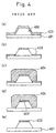
- Fig.1 shows the fabricating process steps in a first embodiment of the present invention.
- This method includes a step of forming a mesa structure M including an active layer and a layer 106 containing aluminum on the topmost part of the mesa structure M by selective growth on a semiconductor substrate 101, a step of oxidizing the layer 106 that contains aluminum so as to form an oxide layer 107, and a step of using the above-noted oxide layer 107 as a mask to grow current blocking layers 108 and 109.
- the optical device fabricated is a semiconductor laser.
- an SiO 2 film having a thickness of 100 nm is fabricated onto a (100) n-type InP substrate 101 by thermal CVD (Fig. 1 (a)).
- a pair of SiO 2 stripes with a pitch of 300 ⁇ m, a width of 5 ⁇ m and a spacing of 1.5 ⁇ m is formed by photolithography and etching with buffered HF (BHF) in the ⁇ 0ll ⁇ direction of the substrate 101.
- BHF buffered HF
- metal organic vapor phase epitaxial (MOVPE) growth is used to grow an n-type InP clad layer 103 (having a thickness of 0.15 ⁇ m and a carrier density of 1 x 10 18 cm -3 ) on the n-type InP substrate 101 patterned as noted above.
- MOVPE metal organic vapor phase epitaxial
- an active layer 104 consisting of an SCH (separate confinement hetero-structure) layer (60 nm on both sides of an MQW layer to be described later) of InGaAsP having a bandgap wavelength of 1.1 ⁇ m, and a MQW (multi-quantum well) layer (emitting wavelength of 1.3 ⁇ m) consisting of seven InGaAsP well layers and six InGaAsP barrier layers.
- the well layers are 1.0 % compressively strained and each has a bandgap wavelength of 1.4 ⁇ m and a thickness of 5 nm.
- Each barrier layer has a bandgap wavelength of 1.1 ⁇ m and a thickness of 10 nm.
- a p-type InP clad layer 105 with a thickness of 0.1 ⁇ m and a carrier density of 7 x 10 17 cm -3 .
- the aforementioned layers are grown in this sequence, over which an InAlAs layer 106 that lattice-matches with InP, is formed to a thickness of 0.1 ⁇ m as the topmost layer.
- SiO 2 mask used in the active layer mesa selective growth is removed using BHF.
- an oxidation step is performed for 20 minutes at 670°C in an N 2 atmosphere that includes steam. Because the InAlAs layer includes aluminum which is at the surface, it is easily oxidized (Fig. 1 (c)), however the other layers, since they do not contain aluminum, are not oxidized. Then, the oxidized InAlAs layer 107 formed by the above-noted process step is used as a mask to grow a p-type InP current blocking layer 108 (with a thickness of 0.75 ⁇ m and a carrier density of 6 x 10 17 cm -3 ) and then grow an n-type InP current blocking layer 109 (with a thickness of 0.6 ⁇ m and a carrier density of 3 x 10 18 cm -3 ) (Fig.
- a p-type InP buried layer 110 (with a thickness of 2 ⁇ m and a carrier density of 1 x 10 18 cm -3 ) and a p-type InGaAs contact layer 111 (with a thickness of 0.3 ⁇ m and a carrier density of 5 x 10 18 cm -3 ) are grown (Fig. 1 (e)), thereby completing the laser structure.
- the composition and the growth rate change correspond to mask width change is utilized. Therefore, the composition and thickness of the layer containing aluminum formed on the topmost part of the active layer mesa will also differ at different parts of the device. Even in such as case, however, by using layer which lattice-matched with the InP substrate, such as is done in this embodiment, even if there is some variation in composition and thickness, it is possible to form a high-quality layer including aluminum.
- a pair of SiO 2 stripes are formed with a pitch of 300 ⁇ m, a width of 5 ⁇ m and a spacing of 1.5 ⁇ m in the ⁇ 0ll ⁇ direction of the n-type GaAs substrate 201, the surface of which is a (100) crystal facet.
- MOVPE metal organic vapor phase epitaxial
- an active layer 204 consisting of an SCH layer (100 nm on both sides of an MQW layer to be described later) of InGaAsP with bandgap wavelength of 0.78 ⁇ m, a MQW layer (emitting wavelength of 0.98 ⁇ m) consisting of five In 0.2 Ga 0.8 As well layers (7 nm thick) and four InGaAsP barrier layers (each 10 nm thick and with a bandgap wavelength of 0.78 ⁇ m), and a p-type InGaP clad layer 205 (with a thickness of 0.1 ⁇ m and a carrier density of 7 x 10 17 cm -3 ) are grown in this sequence, over which an AlAs layer 206 is formed to a thickness of 0.1 ⁇ m as the topmost layer (Fig.
- the SiO 2 mask used in the active layer mesa selective growth is removed using the same method as used in the first embodiment, and the topmost AlAs layer is oxidized (Fig. 2 (c)). In this case, similar to the first embodiment, parts other than the topmost layer are not oxidized.
- the oxidized AlAs layer 207 formed by the above-noted process step is used as a mask to grow a p-type InGaP current blocking layer 208 (with a thickness of 0.75 ⁇ m and a carrier density of 6 x 10 17 cm -3 ) and then grow n-type InGaP current blocking layer 209 (with a thickness of 0.6 ⁇ m and a carrier density of 3 x 10 18 cm -3 ) (Fig. 2 (d)).
- the above-noted oxide layer is removed by selective etching, and then finally a p-type InGaP buried layer 210 (with a thickness of 2 ⁇ m and a carrier density of 1 x 10 18 cm -3 ) and a p-type GaAs contact layer 211 (with a thickness of 0.3 ⁇ m and a carrier density of 5 x 10 18 cm -3 ) are grown, thereby completing the laser structure.
- the composition of InGaP layers are controlled as the lattice constant of those layers matches with that of GaAs.
- the lattice constant of AlAs used on the topmost layer almost matches with that of GaAs and there is no composition change in AlAs layer correspond to a change in mask width.
- SSC-LDs or optical integrated circuits described with regard to the first embodiment it is possible to form a film having a good crystalline structure.
- AlGaAs almost lattice-matches with the GaAs, no problem arises if AlGaAs is used in place of the AlAs noted above.
- a pair of SiO 2 stripes are formed with a pitch of 300 ⁇ m, a width of 5 ⁇ m and a spacing of 1.5 ⁇ m in the ⁇ 0ll ⁇ direction of the n-type InP substrate 301, the surface of which is a (100) crystal facet.
- MOVPE metal organic vapor phase epitaxial
- an active layer 304 consisting of an SCH layer (60 nm on both sides of an MQW layer to be described later) of InAlGaAs with bandgap wavelength of 1.0 ⁇ m and an MQW (multi-quantum well) layer (emitting wavelength of 1.3 ⁇ m) consisting of seven InAlGaAs well layers and six InAlGaAs barrier layers, and a p-type InP clad layer 305 (with a thickness of 0.1 ⁇ m and a carrier density of 7 x 10 17 cm -3 ) are grown in this sequence.
- the aforementioned well layers are 1.0 % compressively strained and each has a thickness of 5 nm and a bandgap wavelength of 1.4 ⁇ m, Each barrier layer has a bandgap wavelength of 1.1 ⁇ m and a thickness of 10 nm.
- an AlAs layer 306 is formed to a thickness of 10 nm as the topmost layer.
- the SiO 2 mask that was used in the active layer mesa selective growth is removed using BHF (Fig. 3 (b)). Then an oxidation step is done for 1 minute at 670°C in an N 2 atmosphere that includes steam, so as to form the oxidized AlAs layer 307.
- the oxidized AlAs layer 307 formed by the above-noted process step is used as a mask to grow a p-type InP current blocking layer 308 (with a thickness of 0.75 ⁇ m and a carrier density of 6 x 10 17 cm -3 ) and then grow n-type InP current blocking layer 309 (with a thickness of 0.6 ⁇ m and a carrier density of 3 x 10 18 cm -3 ) (Fig. 3 (d)).
- the above-noted oxide layer 307 is removed by selective etching, and then finally a p-type InP buried layer 310 (with a thickness of 2 ⁇ m and a carrier density of 1 x 10 18 cm -3 ) and a p-type InGaAs contact layer 311 (with a thickness of 0.3 ⁇ m and a carrier density of 5 x 10 18 cm -3 ) are grown, thereby completing the laser structure (Fig. 3 (e)).
- the topmost AlAs layer includes only Al as a Group III element, it is extremely easily oxidized in a short time. In particular, by forming a thin AlAs layer, this time can be further shortened. By shortening the oxidation time in this manner, even if a layer including aluminum, such as the active layer or SCH layer in this embodiment is used, it is possible to oxidize just the topmost part. Additionally, it should be noted that, although the lattice constant of AlAs layer at the topmost part in this embodiment does not match with that of the InP substrate, it is possible to grow the AlAs layer without lattice mismatch distortion if the film is made sufficiently thin. In the case of an AlGaAs, AlInGaAs, or AlGaInP laser grown on a GaAs substrate, because the AlAs almost completely lattice-matches with GaAs, there is almost no problem.
- the present invention is not restricted the above-described embodiments, and can take on numerous variant forms within the spirit of the present invention.
- a bulk layer including aluminum was used as the topmost layer of an active mesa in the above-described embodiments, there is no restriction to a bulk layer, and a superlattice made of AlAs or AlInAs can be applied as well.
- n-type substrate is used, it will be obvious that the present invention can be applied to the fabrication of a laser on a p-type substrate as well. In which case, of course, it is necessary to have the conduction type of each layer reversed to accommodate this change in substrate conductivity type.
- InGaAsP or InAlGaAs laser is formed on an InP substrate or the case in which an InGaAsP laser is formed on a GaAs substrate, it is also possible to use a material such as InGaAlP or InGaNAs as the active layer.
- a substrate of InP or GaAs it is further possible to apply the present invention to the case of a AlInGaN laser on a GaN substrate.
- the present invention is not limited in application to semiconductor lasers, and can also be applied to the fabrication of a variety of optical integrated circuits, such as semiconductor optical amplifiers, modulators, and optical integrated circuit combined those devices.
Landscapes
- Physics & Mathematics (AREA)
- Geometry (AREA)
- Condensed Matter Physics & Semiconductors (AREA)
- General Physics & Mathematics (AREA)
- Electromagnetism (AREA)
- Optics & Photonics (AREA)
- Semiconductor Lasers (AREA)
Applications Claiming Priority (2)
| Application Number | Priority Date | Filing Date | Title |
|---|---|---|---|
| JP1692499 | 1999-01-26 | ||
| JP11016924A JP2000216495A (ja) | 1999-01-26 | 1999-01-26 | 半導体光素子の製造方法 |
Publications (2)
| Publication Number | Publication Date |
|---|---|
| EP1024565A2 true EP1024565A2 (fr) | 2000-08-02 |
| EP1024565A3 EP1024565A3 (fr) | 2000-11-22 |
Family
ID=11929686
Family Applications (1)
| Application Number | Title | Priority Date | Filing Date |
|---|---|---|---|
| EP00101538A Withdrawn EP1024565A3 (fr) | 1999-01-26 | 2000-01-26 | Dispositif optique semi-conducteur et méthode de fabrication |
Country Status (4)
| Country | Link |
|---|---|
| US (1) | US6261855B1 (fr) |
| EP (1) | EP1024565A3 (fr) |
| JP (1) | JP2000216495A (fr) |
| KR (1) | KR20000053604A (fr) |
Cited By (2)
| Publication number | Priority date | Publication date | Assignee | Title |
|---|---|---|---|---|
| EP1227361A3 (fr) * | 2001-01-30 | 2004-05-26 | The Furukawa Electric Co., Ltd. | Dispositif optique à semi-conducteur ayant une capacité parasite réduite |
| CN109192806A (zh) * | 2018-08-30 | 2019-01-11 | 武汉电信器件有限公司 | 一种光电探测器及其制作方法 |
Families Citing this family (3)
| Publication number | Priority date | Publication date | Assignee | Title |
|---|---|---|---|---|
| US6531414B1 (en) * | 1999-05-05 | 2003-03-11 | The United States Of America As Represented By The National Security Agency | Method of oxidizing strain-compensated superlattice of group III-V semiconductor |
| US6664605B1 (en) * | 2000-03-31 | 2003-12-16 | Triquint Technology Holding Co. | Dopant diffusion blocking for optoelectronic devices using InAlAs and/or InGaAlAs |
| FR2820891B1 (fr) * | 2001-02-13 | 2004-08-27 | Cit Alcatel | Laser semi conducteur a ruban enterre et procede de fabrication |
Family Cites Families (13)
| Publication number | Priority date | Publication date | Assignee | Title |
|---|---|---|---|---|
| US4230997A (en) * | 1979-01-29 | 1980-10-28 | Bell Telephone Laboratories, Incorporated | Buried double heterostructure laser device |
| JPS60117631A (ja) * | 1983-11-30 | 1985-06-25 | Toshiba Corp | 化合物半導体のドライエッチング方法 |
| JPH01313985A (ja) * | 1988-06-14 | 1989-12-19 | Fujitsu Ltd | 半導体発光装置の製造方法 |
| JP2963916B2 (ja) | 1988-12-28 | 1999-10-18 | 新技術事業団 | 面発光型半導体レーザ装置の製造方法 |
| JPH04243216A (ja) * | 1991-01-17 | 1992-08-31 | Nec Corp | 光導波路の製造方法ならびに光集積素子及びその製造方法 |
| JPH0513876A (ja) * | 1991-07-04 | 1993-01-22 | Mitsubishi Electric Corp | 半導体レーザの製造方法 |
| JP2998629B2 (ja) | 1995-03-31 | 2000-01-11 | 日本電気株式会社 | 光半導体装置とその製造方法 |
| US5847415A (en) * | 1995-03-31 | 1998-12-08 | Nec Corporation | Light emitting device having current blocking structure |
| US5568499A (en) * | 1995-04-07 | 1996-10-22 | Sandia Corporation | Optical device with low electrical and thermal resistance bragg reflectors |
| US5869849A (en) * | 1995-10-05 | 1999-02-09 | Industry Technology Research Institute | Light-emitting diodes with high illumination |
| JPH1075009A (ja) | 1996-08-30 | 1998-03-17 | Nec Corp | 光半導体装置とその製造方法 |
| JPH10215023A (ja) | 1996-11-29 | 1998-08-11 | Victor Co Of Japan Ltd | 内部電流狭窄型半導体レ−ザ素子の製造方法 |
| JP3104789B2 (ja) | 1997-05-02 | 2000-10-30 | 日本電気株式会社 | 半導体光素子およびその製造方法 |
-
1999
- 1999-01-26 JP JP11016924A patent/JP2000216495A/ja active Pending
-
2000
- 2000-01-25 KR KR1020000003412A patent/KR20000053604A/ko not_active Ceased
- 2000-01-26 EP EP00101538A patent/EP1024565A3/fr not_active Withdrawn
- 2000-01-26 US US09/491,630 patent/US6261855B1/en not_active Expired - Fee Related
Cited By (2)
| Publication number | Priority date | Publication date | Assignee | Title |
|---|---|---|---|---|
| EP1227361A3 (fr) * | 2001-01-30 | 2004-05-26 | The Furukawa Electric Co., Ltd. | Dispositif optique à semi-conducteur ayant une capacité parasite réduite |
| CN109192806A (zh) * | 2018-08-30 | 2019-01-11 | 武汉电信器件有限公司 | 一种光电探测器及其制作方法 |
Also Published As
| Publication number | Publication date |
|---|---|
| EP1024565A3 (fr) | 2000-11-22 |
| US6261855B1 (en) | 2001-07-17 |
| JP2000216495A (ja) | 2000-08-04 |
| KR20000053604A (ko) | 2000-08-25 |
Similar Documents
| Publication | Publication Date | Title |
|---|---|---|
| US7941024B2 (en) | Buried heterostructure device having integrated waveguide grating fabricated by single step MOCVD | |
| EP0702435A1 (fr) | Méthode de fabrication d'un laser accordable de façon numérique par réflection | |
| JP2827326B2 (ja) | 半導体レーザの製造方法 | |
| JPH07221392A (ja) | 量子細線の作製方法、量子細線、量子細線レーザ、及び量子細線レーザの作製方法、回折格子の作製方法、及び分布帰還型半導体レーザ | |
| US5260230A (en) | Method of manufacturing buried heterostructure semiconductor laser | |
| EP0114109B1 (fr) | Dispositif laser à semi-conducteur et son procédé de fabrication | |
| US5602866A (en) | Semiconductor laser | |
| US6261855B1 (en) | Method for fabricating a semiconductor optical device | |
| EP1198043A2 (fr) | Méthode de fabrication d'un dispositif semiconducteur en composé III-V comprenant une couche d'un composé d'Aluminium | |
| US7184640B2 (en) | Buried heterostructure device fabricated by single step MOCVD | |
| JP2950028B2 (ja) | 光半導体素子の製造方法 | |
| JP3317271B2 (ja) | 半導体光素子およびその製造方法 | |
| US5805628A (en) | Semiconductor laser | |
| JP2911751B2 (ja) | 半導体レーザ及びその製造方法 | |
| JP2001077465A (ja) | 半導体レーザ及びその製造方法 | |
| JPH077232A (ja) | 光半導体装置 | |
| JPH05299764A (ja) | 半導体レーザの製造方法 | |
| JP2917695B2 (ja) | 光半導体素子の製造方法 | |
| JP2708949B2 (ja) | 半導体レーザ装置の製造方法 | |
| JPH11126945A (ja) | 歪み半導体結晶の製造方法、これを用いた半導体レーザの製造方法 | |
| JPH1022564A (ja) | 半導体レーザ、半導体光変調器および半導体レーザの製造方法 | |
| JP3022351B2 (ja) | 光半導体装置及びその製造方法 | |
| JPH03185889A (ja) | 半導体レーザ素子およびその製造方法 | |
| JPH09186391A (ja) | 化合物半導体装置及びその製造方法 | |
| JPH05235477A (ja) | 光半導体素子の製造方法 |
Legal Events
| Date | Code | Title | Description |
|---|---|---|---|
| PUAI | Public reference made under article 153(3) epc to a published international application that has entered the european phase |
Free format text: ORIGINAL CODE: 0009012 |
|
| AK | Designated contracting states |
Kind code of ref document: A2 Designated state(s): DE FR |
|
| AX | Request for extension of the european patent |
Free format text: AL;LT;LV;MK;RO;SI |
|
| PUAL | Search report despatched |
Free format text: ORIGINAL CODE: 0009013 |
|
| AK | Designated contracting states |
Kind code of ref document: A3 Designated state(s): DE FR |
|
| AX | Request for extension of the european patent |
Free format text: AL;LT;LV;MK;RO;SI |
|
| RIC1 | Information provided on ipc code assigned before grant |
Free format text: 7H 01S 5/227 A, 7H 01S 5/323 B, 7H 01L 33/00 B, 7H 01S 3/19 B |
|
| 17P | Request for examination filed |
Effective date: 20001018 |
|
| 17Q | First examination report despatched |
Effective date: 20010315 |
|
| AKX | Designation fees paid |
Free format text: DE FR |
|
| STAA | Information on the status of an ep patent application or granted ep patent |
Free format text: STATUS: THE APPLICATION HAS BEEN WITHDRAWN |
|
| 18W | Application withdrawn |
Effective date: 20030317 |