EP1025640B1 - Integrierte elektroische schaltung mit einem oszilltor und passiven schaltungsbauteilen - Google Patents
Integrierte elektroische schaltung mit einem oszilltor und passiven schaltungsbauteilen Download PDFInfo
- Publication number
- EP1025640B1 EP1025640B1 EP98950557A EP98950557A EP1025640B1 EP 1025640 B1 EP1025640 B1 EP 1025640B1 EP 98950557 A EP98950557 A EP 98950557A EP 98950557 A EP98950557 A EP 98950557A EP 1025640 B1 EP1025640 B1 EP 1025640B1
- Authority
- EP
- European Patent Office
- Prior art keywords
- conductor
- electronic circuit
- circuit according
- antenna elements
- receiver
- Prior art date
- Legal status (The legal status is an assumption and is not a legal conclusion. Google has not performed a legal analysis and makes no representation as to the accuracy of the status listed.)
- Expired - Lifetime
Links
Images

Classifications
-
- H—ELECTRICITY
- H01—ELECTRIC ELEMENTS
- H01Q—ANTENNAS, i.e. RADIO AERIALS
- H01Q3/00—Arrangements for changing or varying the orientation or the shape of the directional pattern of the waves radiated from an antenna or antenna system
- H01Q3/26—Arrangements for changing or varying the orientation or the shape of the directional pattern of the waves radiated from an antenna or antenna system varying the relative phase or relative amplitude of energisation between two or more active radiating elements; varying the distribution of energy across a radiating aperture
- H01Q3/2682—Time delay steered arrays
-
- H—ELECTRICITY
- H10—SEMICONDUCTOR DEVICES; ELECTRIC SOLID-STATE DEVICES NOT OTHERWISE PROVIDED FOR
- H10D—INORGANIC ELECTRIC SEMICONDUCTOR DEVICES
- H10D84/00—Integrated devices formed in or on semiconductor substrates that comprise only semiconducting layers, e.g. on Si wafers or on GaAs-on-Si wafers
- H10D84/201—Integrated devices formed in or on semiconductor substrates that comprise only semiconducting layers, e.g. on Si wafers or on GaAs-on-Si wafers characterised by the integration of only components covered by H10D1/00 or H10D8/00, e.g. RLC circuits
- H10D84/204—Integrated devices formed in or on semiconductor substrates that comprise only semiconducting layers, e.g. on Si wafers or on GaAs-on-Si wafers characterised by the integration of only components covered by H10D1/00 or H10D8/00, e.g. RLC circuits of combinations of diodes or capacitors or resistors
- H10D84/206—Integrated devices formed in or on semiconductor substrates that comprise only semiconducting layers, e.g. on Si wafers or on GaAs-on-Si wafers characterised by the integration of only components covered by H10D1/00 or H10D8/00, e.g. RLC circuits of combinations of diodes or capacitors or resistors of combinations of capacitors and resistors
-
- H—ELECTRICITY
- H10—SEMICONDUCTOR DEVICES; ELECTRIC SOLID-STATE DEVICES NOT OTHERWISE PROVIDED FOR
- H10W—GENERIC PACKAGES, INTERCONNECTIONS, CONNECTORS OR OTHER CONSTRUCTIONAL DETAILS OF DEVICES COVERED BY CLASS H10
- H10W20/00—Interconnections in chips, wafers or substrates
- H10W20/40—Interconnections external to wafers or substrates, e.g. back-end-of-line [BEOL] metallisations or vias connecting to gate electrodes
-
- H—ELECTRICITY
- H10—SEMICONDUCTOR DEVICES; ELECTRIC SOLID-STATE DEVICES NOT OTHERWISE PROVIDED FOR
- H10W—GENERIC PACKAGES, INTERCONNECTIONS, CONNECTORS OR OTHER CONSTRUCTIONAL DETAILS OF DEVICES COVERED BY CLASS H10
- H10W20/00—Interconnections in chips, wafers or substrates
- H10W20/40—Interconnections external to wafers or substrates, e.g. back-end-of-line [BEOL] metallisations or vias connecting to gate electrodes
- H10W20/497—Inductive arrangements or effects of, or between, wiring layers
Definitions
- the invention rotates to an integrated electronic circuit with at least one active electronic component and a delay element, according to the opening portion of claim 1.
- a well-known way to set up an oscillator is to feed back a gate circuit with an inverter function, for example a simple inverter, via some form of time delay.
- the time delay can be implemented in various ways, for example by special delay circuits.
- crystal oscillator In applications where high working frequencies are used, and particularly when the requirements of a frequency-stable oscillator are high, a. crystal oscillator is used instead.
- a problem with use of crystal oscillators is that they are relatively large. In connection with certain types of integrated circuits this becomes a problem in that a special circuit must be used with the oscillator or a crystal must be connected from outside the integrated circuit.
- antennas for transmission and reception of electromagnetic signals are used with a special embodiment for exploiting signals for strong directional effects.
- the currency most common type of antenna in this connection is the parabolic antenna.
- So-called electronically controlled antennas or phase array antennas are becoming more common.
- a phase array antenna incorporates a group of identical radiation elements. By controlled feeding of the elements by means of a conductor network so that they act in phase, an electromagnetic beam with good directionality can be achieved.
- the conductor network can also incorporate electronically controlled phase inverters and possibly amplifiers, one for each element, by means of which the direction of the beam can be varied without need of mechanically moveable components.
- phase inverters are complicated and expensive instruments, and for that reason this type of antenna has not enjoyed great commercial success. Another factor which limits the use of this type of antenna is the frequency dependency of the phase inverters. The foremost area of use for the phase array antenna is within the radar area.
- An integrated electronic circuit according to the preamble of claim 1 is known from US-A- A-5 652 549.
- It is an object of the invention is to produce an electronic circuit that can be embodied in a simple manner and that can be combined with other circuits in an integrated form.
- an oscillator has been achieved that is realizable in all components in integrated form.
- an electronically controlled antenna has been achieved that lacks the disadvantages of the phase inverters.
- the purpose is achieved by the fact that electronic signals from individual antenna elements are differentially delayed dependent on the position of the antenna elements in relation to the impinging electromagnetic wave fronts. Emanating from one matrix of the antenna elements that are distributed across a surface, the signals can be selectively delayed from individual antenna elements and thus affect the direction in which the antenna will be sensitive.
- the delay is preferably produced in integrated circuits, which are provided in connection with the antenna elements.
- an installation of conductors of different length is provided between the antenna elements and a receiving unit.
- a conductor of a certain length is switched on by a control unit dependent on the position of the antenna element in relation to an impinging wave front of an electromagnetic wave.
- the given position affects the detectable characteristics of the electric signals that are received.
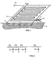
- an inverter coupling 10 is shown schematically, whose input 11 is connected to its output 12 via a long conductor 13.
- the frequency is 200MHz. This is under the condition that the delay in the inverter coupling itself is on the magnitude of some picoseconds. With low propagation in the inverter coupling's delay of, for example, 10% the inaccuracy is in the same class as that of a crystal oscillator. This length required for attainment of the desired delay acts in many cases as a deterrent. The actually delay in the conductor is also dependent on the conductor's distributed resistance and the conductor's distributed capacitance.
- the conductor is embodied as a metal conductor in an integrated process, for example a CMOS process.
- Conductor 13 is embodied with width w and rests on some form of insulating layer 14.
- the insulating layer contains both metal oxide and field oxide and has thickness b.
- Inverter coupling 10 and other semiconductor circuits can be embodied in semiconducting materials, whereby these are given access to the oscillator.
- the insulating layer is constituted of silicon oxide.
- the insulating layer can also be embodied in glass or another ceramic material.
- the insulating layer can be embodied as an air layer.
- the conductor rests on stanchion-like formations that extend from the semiconductor or base material used.
- the conductor is embodied so that it gives rise to as little inductance as possible.
- the conductor runs in a loop with several parallel conductor sections so that the directions of the current in adjacent conductor sections are opposite to each other. It is also possible to provide two parallel loops in opposition or in double loops.
- t RC ⁇ 0 n R n ⁇ C n when n ⁇ ⁇
- K rc ⁇ ⁇ ⁇ a ⁇ b
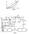
- the diagram in fIG 3 with the curve t A shows the delay that depends on the velocity of propagation in the conductor
- the curve t RC shows the delay that depends on the resistance R of the conductor and capacitance C. The velocity of propagation in the conductor cannot be affected to any great degree.
- insutation layer 14 is embodied preferably with significantly greater thickness b than the occurring oxide layer.
- a suitable thickness exceeds 10 ⁇ m and is preferably in the range of 10-100 ⁇ m if the oscillator is to be used at frequencies around 1 GHz.
- the thickness w of conductor 13 is in commonly occurring processes around 1 ⁇ m, and an increase in thickness, but not width, improves the oscillator's characteristics and performance.
- the length of the conductor It is thus not suitable to embody the conductor in a spiral form or similar.
- the length should also be suited to the desired wavelength of the oscillator.
- the length of the conductor preferably amounts to a multiple of the half wavelength or, more preferably, half the wavelength.
- the invention comprises antenna elements 16, which are connected to a cell unit 22.
- Cell unit 22 which is designated by dashed lines in FIG 4, contains an installation of individually switchable delay-elements 18, by means of which a signal received in antenna element 16 is directed on to a receiver 17 acting in common for a number of cell units 22.
- the received signal is amplified in an amplifier 23.
- Delay elements 18 in the form of conductors connect demultiplexer 19 and multiplexer 21, and an individual delay element 18 is switched by means of adjustment of demultiplexer 19 and/or multiplexer 21. Adjustment is done by a control unit 20, which is connected to a central processing unit (CPU) 24 in common for several cell units 22.
- CPU central processing unit
- the incoming signal can have a frequency on the order of magnitude of 12 GHz
- the incoming signal is preferably merged with a signal from a local oscillator 25 and sent.to a mixer 26. From mixer 26 the signal suitably has a frequency on the order of magnitude of some GHz.
- the different control units 20 and possibly also the local oscillators 25 are connected to a CPU 24, preferably by a buss connection 27. It can be suitable to include in CPU 24 means for synchronization of the different oscillators 25. Synchronization can also occur via control unit 20.
- the oscillator is not included in the cell unit. A common oscillator is instead preferably located in the CPU. The embodiment of the oscillator used should be adjustable for different frequency bands.
- All components, which are included in cell unit 22, can be embodied to be integrated in semiconducting materials.
- the semiconductor process used should be selected with regard to high frequency characteristics, especially as regards amplifier 23, and to characteristics that affect conductors that can be included in the delay elements.
- the noise ratio should be on the order of magnitude of 0.5 dBu.
- Very low capacity switches should be sought.
- the conductor is embodied as a metal conductor in an integrated process, for example a CMOS process.
- Receiver 17 can be embodied in a conventional way as a satellite receiver. It can be the case that satellite receivers are provided with control instruments for motorized control of a conventional parabola antenna. Receiver 17 includes similar control instruments, and a control output 28 transfers control information to CPU 24.
- the control information can include instructions to sweep with the electrically controlled antenna across a certain arc in connection with finding a new transmitter. When a transmitter is found, the control information will continuously control the adjustment of the antenna so that the transmitter can be followed if the antenna is physically angled or displaced in relation to the transmitter.
- a signal conductor 29, preferably from each of the cell units 22, conducts a received signal from the antenna to receiver 17.
- the quality and certain characteristics of the signal from the antenna affect how CPU 24 will be controlled in turn in order to affect the different control units 20 in the cell units 22.
- the number of delay elements 18, which are required in order that the desired possibilities for fine tuning of the antenna can be achieved, varies with the current application. For normal satellite receiver application some hundreds of delay elements 18 should be sufficient.
- the characteristics of amplifier 23 also affect how many delay elements 18 are required. With very good amplification characteristics and signal-noise relation in the amplifier the number of directionally adjusting delay elements 18 can be held down.
- An antenna embodied with components according to the above can be embodied as indicated by FIG 5.
- Provided on a surface are a number of cell units 22. Every cell unit 22 is connected to four antenna elements 16A-16D attached in pairs. Two opposing first antenna elements 16A and 16B are dedicated to reception of horizontally polarized signals, and two opposing second antenna elements 16C and 16D are dedicated to reception of vertically polarized signals. Other configurations can also be used for reception of different types of signals. Every antenna element 16A-16D can be some millimeters long and wide, and different forms can occur. Antenna elements 16A-16D are preferably embodied of metal. The outer dimensions of the antenna with a suitable number of antenna elements can be such that the surface of the antenna is on the order of magnitude of 0.1-1.0 m 2 .
- Buss connection 27 preferably runs through or past each cell unit 22.
- the different antenna elements 16A-16D can be attached to amplifier 23 directly or via a multiplexer, which is suitably controlled by control unit 20.
- FIG 6 shows in principle how conductors 18 can be embodied.
- Each conductor 18 is embodied with width w and rests on some form of insulating layer 14.
- the insulating layer is normally comprised of both metal oxide and field oxide and had thickness b.
- amplifier 23 and further semiconductor circuits can be embodied.
- the insulating layer is made of silicon oxide.
- the insulating layer can also be embodied of glass.
- the insulating layer can be embodied as a layer of air. In such an embodiment the conductor rests on stanchion-like formations which emerge from the semiconductive or base material used.
- a suitable thickness exceeds 10 ⁇ m and preferably lies in the range of 10-100 ⁇ m, if the apparatus is to be used at frequencies around some GHz.
- the thickness of the conductor is in normally occurring processes around 1 ⁇ m, and an increase of thickness, but not of width, improves the characteristics and performance of the delay elements.
Landscapes
- Semiconductor Integrated Circuits (AREA)
- Variable-Direction Aerials And Aerial Arrays (AREA)
- Design And Manufacture Of Integrated Circuits (AREA)
- Inductance-Capacitance Distribution Constants And Capacitance-Resistance Oscillators (AREA)
- Oscillators With Electromechanical Resonators (AREA)
- Coils Or Transformers For Communication (AREA)
Claims (17)
- Integrierter Elektronikschaltkreis mit einem von einem elektrischen Leiter (13, 18) gebildeten Verzögerungselement und mit mindestens einem aktiven elektronischen Bauteil (10, 21), das mit dem elektrischen Leiter (13, 18) verbunden ist, wobei
der Leiter (13, 18) derart ausgebildet ist, dass seine Induktivität auf ein Minimum reduziert wird, d.h. in einer Schleife mit parallelen Leiterabschnitten, so dass die Richtungen des Stroms in angrenzenden Leiterabschnitten entgegengesetzt zueinander sind, und
der Leiter (13, 18) aus einem leitfähigen Werkstoff auf einer Isolierschicht (14) gebildet wird, dadurch gekennzeichnet,
dass die Isolierschicht (14) von Halbleiterwerkstoff (15) umgeben ist und die Dicke der Isolierschicht (14) 10µm überschreitet, so dass eine geringe kapazitive Kopplung zwischen dem Leiter (13, 18) und dem umgebenden Halbleiterwerkstoff geschaffen wird. - Elektronikschaltkreis nach Anspruch 1, dadurch gekennzeichnet,
dass das elektronische Bauteil einen Inverter (10) mit einem Eingang (11) und einem Ausgang (12) aufweist, und
dass der Leiter (13) dazu vorgesehen ist, den Eingang (11) mit dem Ausgang (12) zu verbinden, wodurch ein Oszillator geschaffen wird. - Elektronikschaltkreis nach Anspruch 1, dadurch gekennzeichnet,
dass sich die Isolierschicht (14) aus Oxid-Werkstoff zusammensetzt. - Elektronikschaltkreis nach Anspruch 2, dadurch gekennzeichnet,
dass der Inverter (10) und der Leiter (13) in einem Halbleiterverfahren mit Halbleitern/Metall auf Glas/Keramik hergestellt werden. - Elektronikschaltkreis nach Anspruch 1, dadurch gekennzeichnet,
dass sich die Isolierschicht (14) aus Luft zusammensetzt. - Elektronikschaltkreis nach Anspruch 1, dadurch gekennzeichnet,
dass die Dicke der Isolierschicht (14) 20µm überschreitet. - Elektronikschaltkreis nach Anspruch 1, dadurch gekennzeichnet,
dass die Dicke des Leiters (13) 1 µm überschreitet. - Elektronikschaltkreis nach Anspruch 2, dadurch gekennzeichnet,
dass der Inverter (10) aus Halbleiterwerkstoff hergestellt ist. - Elektronikschaltkreis nach Anspruch 2, dadurch gekennzeichnet,
dass der Inverter (10) in einem Verfahren hergestellt wird, welches Silizium auf dem Isolator aufweist. - Elektronikschaltkreis nach Anspruch 1, dadurch gekennzeichnet,
dass die Länge des Leiters (13) 0,2m überschreitet. - Elektronikschaltkreis mit einer elektronisch gesteuerten Antenne, einem Empfänger (17) und einer Reihe von mit dem Empfänger (17) verbundenen Antennenelementen (16), dadurch gekennzeichnet,
dass individuelle Antennenelemente (16) mit dem Empfänger (17) über einen integrierten Elektronikschaltkreis gemäß Anspruch 1 verbunden sind, welcher automatisch auswählbare Verzögetungselemente (18) aufweist, so dass elektrische Signale von unterschiedlichen Antennenelementen (16) abhängig von der Position der Antennenelemente im Hinblick auf die einfallenden elektromagnetischen Wellenfronten unterschiedlich verzögert werden. - Elektronikschaltkreis nach Anspruch 11, dadurch gekennzeichnet,
dass die Verzögerungselemente (18) elektrische Leiter unterschiedlicher Länge aufweisen. - Elektronikschaltkreis nach Anspruch 11, dadurch gekennzeichnet,
dass individuelle Antennenelemente (16) über einen Demultiplexer (19) an die Verzögerungselemente (18) angeschlossen sind,
dass individuelle Antennenelemente (16) über'einem Multiplexer (21) an den Empfänger (17) angeschlossen sind, und
dass der Demultiplexer (19) betriebsbereit an eine Steuereinheit (20) angeschlossen ist, so dass ein individuelles Verzögerungselement (18) abhängig von den Eigenschaften der empfangenen elektrischen Signale geschaltet wird. - Elektronikschaltkreis nach Anspruch 13, dadurch gekennzeichnet,
dass der Demultiplexer (19), der Multiplexer (21) sowie die Steuereinheit (20) zusammen mit den Verzögerungselementen (18) in einer Zelleneinheit (22) bereitgestellt werden, wobei die Zelleneinheit als integrierter Schaltkreis ausgebildet ist, und
dass ein Antennenelement (16) mit einer Zelleneinheit (22) verbunden ist. - Elektronikschaltkreis nach Anspruch 13, dadurch gekennzeichnet,
dass der Empfänger (17) an eine Zentraleinheit (24) zur Übertragung von Steuerinformationen zum Steuern der Antenne angeschlossen ist, und
dass die Zentraleinheit (24) an die mit den Antennenelementen (16) verbundenen Steuereinheiten (20) angeschlossen ist. - Elektronikschaltkreis nach Anspruch 13, dadurch gekennzeichnet,
dass individuelle Antennenelemente (16) über einen Verstärker (23) mit dem Demultiplexer (19) verbunden sind. - Elektronikschaltkreis nach Anspruch 13, dadurch gekennzeichnet,
dass individuelle Antennenelemente (16) über einen Mischer (26) mit dem Demultiplexer (19) verbunden sind, und
dass der Mischer (26) auch an einen Oszillator (25) angeschlossen ist.
Applications Claiming Priority (5)
| Application Number | Priority Date | Filing Date | Title |
|---|---|---|---|
| SE9703843 | 1997-10-22 | ||
| SE9703843A SE523414C2 (sv) | 1997-10-22 | 1997-10-22 | Oscillator |
| SE9704561A SE518928C2 (sv) | 1997-12-08 | 1997-12-08 | Elektroniskt styrd antenn |
| SE9704561 | 1997-12-08 | ||
| PCT/SE1998/001829 WO1999021274A2 (en) | 1997-10-22 | 1998-10-12 | Integrated electronic circuit comprising an oscillator with passive circuit elements |
Publications (2)
| Publication Number | Publication Date |
|---|---|
| EP1025640A2 EP1025640A2 (de) | 2000-08-09 |
| EP1025640B1 true EP1025640B1 (de) | 2006-03-22 |
Family
ID=26663108
Family Applications (1)
| Application Number | Title | Priority Date | Filing Date |
|---|---|---|---|
| EP98950557A Expired - Lifetime EP1025640B1 (de) | 1997-10-22 | 1998-10-12 | Integrierte elektroische schaltung mit einem oszilltor und passiven schaltungsbauteilen |
Country Status (9)
| Country | Link |
|---|---|
| US (1) | US6486829B1 (de) |
| EP (1) | EP1025640B1 (de) |
| JP (1) | JP4502501B2 (de) |
| AT (1) | ATE321374T1 (de) |
| AU (1) | AU9656598A (de) |
| DE (1) | DE69833960T2 (de) |
| ES (1) | ES2259819T3 (de) |
| NO (1) | NO321209B1 (de) |
| WO (1) | WO1999021274A2 (de) |
Families Citing this family (5)
| Publication number | Priority date | Publication date | Assignee | Title |
|---|---|---|---|---|
| SE9901665D0 (sv) * | 1999-05-05 | 1999-05-05 | Avancerade Logikmaskiner Ab | Fördröjningskrets |
| US7099956B2 (en) * | 2000-01-31 | 2006-08-29 | Ideaflood, Inc. | Method and apparatus for conducting domain name service |
| US20020019800A1 (en) * | 2000-05-16 | 2002-02-14 | Ideaflood, Inc. | Method and apparatus for transacting divisible property |
| WO2011055103A1 (en) * | 2009-11-06 | 2011-05-12 | John Wood | A clock arrangement in an integrated circuit |
| JP7795386B2 (ja) * | 2022-03-17 | 2026-01-07 | 株式会社豊田中央研究所 | オンチップアンテナ |
Family Cites Families (15)
| Publication number | Priority date | Publication date | Assignee | Title |
|---|---|---|---|---|
| CA1253959A (en) * | 1985-12-11 | 1989-05-09 | Paul I. Pulsifer | Phased array antenna feed |
| JPH0377360A (ja) | 1989-08-18 | 1991-04-02 | Mitsubishi Electric Corp | 半導体装置 |
| FR2651609B1 (fr) | 1989-09-01 | 1992-01-03 | Thomson Csf | Commande de pointage pour systeme d'antenne a balayage electronique et formation de faisceau par le calcul. |
| US5013979A (en) * | 1989-12-29 | 1991-05-07 | Texas Instrument Incorporated | Phased frequency steered antenna array |
| JPH0440003A (ja) * | 1990-06-05 | 1992-02-10 | Mitsubishi Electric Corp | 多層化アレイアンテナ |
| US5105200A (en) * | 1990-06-18 | 1992-04-14 | Ball Corporation | Superconducting antenna system |
| US5063390A (en) | 1991-02-19 | 1991-11-05 | The United States Of America As Represented By The Secretary Of The Army | Non-dispersive acoustic transport time delay beam steering antenna |
| US5518674A (en) * | 1991-06-28 | 1996-05-21 | Texas Instruments Incorporated | Method of forming thin film flexible interconnect for infrared detectors |
| WO1994017558A1 (en) * | 1993-01-29 | 1994-08-04 | The Regents Of The University Of California | Monolithic passive component |
| JP2513405B2 (ja) * | 1993-06-11 | 1996-07-03 | 日本電気株式会社 | 2周波共用アレイアンテナ |
| JP2750268B2 (ja) * | 1993-12-21 | 1998-05-13 | 株式会社エイ・ティ・アール光電波通信研究所 | マイクロ波集積回路付きアンテナ装置の製造方法 |
| DE19511401A1 (de) * | 1995-03-28 | 1996-10-10 | Siemens Ag | Monolithisch integrierter Oszillator |
| JP3077056B2 (ja) * | 1996-09-12 | 2000-08-14 | 株式会社村田製作所 | 積層型電子部品 |
| US5757319A (en) * | 1996-10-29 | 1998-05-26 | Hughes Electronics Corporation | Ultrabroadband, adaptive phased array antenna systems using microelectromechanical electromagnetic components |
| US5834945A (en) * | 1996-12-31 | 1998-11-10 | Micron Technology, Inc. | High speed temporary package and interconnect for testing semiconductor dice and method of fabrication |
-
1998
- 1998-10-12 EP EP98950557A patent/EP1025640B1/de not_active Expired - Lifetime
- 1998-10-12 DE DE69833960T patent/DE69833960T2/de not_active Expired - Lifetime
- 1998-10-12 AU AU96565/98A patent/AU9656598A/en not_active Abandoned
- 1998-10-12 ES ES98950557T patent/ES2259819T3/es not_active Expired - Lifetime
- 1998-10-12 JP JP2000517481A patent/JP4502501B2/ja not_active Expired - Fee Related
- 1998-10-12 WO PCT/SE1998/001829 patent/WO1999021274A2/en not_active Ceased
- 1998-10-12 AT AT98950557T patent/ATE321374T1/de not_active IP Right Cessation
-
2000
- 2000-04-12 US US09/548,058 patent/US6486829B1/en not_active Expired - Fee Related
- 2000-04-13 NO NO20001941A patent/NO321209B1/no not_active IP Right Cessation
Also Published As
| Publication number | Publication date |
|---|---|
| NO20001941D0 (no) | 2000-04-13 |
| NO321209B1 (no) | 2006-04-03 |
| WO1999021274A3 (en) | 1999-07-01 |
| DE69833960D1 (de) | 2006-05-11 |
| AU9656598A (en) | 1999-05-10 |
| DE69833960T2 (de) | 2006-11-30 |
| EP1025640A2 (de) | 2000-08-09 |
| NO20001941L (no) | 2000-05-15 |
| US6486829B1 (en) | 2002-11-26 |
| ES2259819T3 (es) | 2006-10-16 |
| JP4502501B2 (ja) | 2010-07-14 |
| ATE321374T1 (de) | 2006-04-15 |
| JP2001521292A (ja) | 2001-11-06 |
| WO1999021274A2 (en) | 1999-04-29 |
Similar Documents
| Publication | Publication Date | Title |
|---|---|---|
| US4573212A (en) | Integrated receiver antenna device | |
| US5940030A (en) | Steerable phased-array antenna having series feed network | |
| US6741141B2 (en) | Ultra wideband frequency dependent attenuator with constant group delay | |
| US5115217A (en) | RF tuning element | |
| US8138989B2 (en) | Transmission line distributed oscillator | |
| US7884776B2 (en) | High power integrated circuit beamforming array | |
| US6219002B1 (en) | Planar antenna | |
| KR101126642B1 (ko) | 반사 안테나 | |
| KR20080051180A (ko) | 칩 안테나 상 ㎜-파 완전 집적 위상 어레이 수신기 및송신기 | |
| Abdalla et al. | A planar electronically steerable patch array using tunable PRI/NRI phase shifters | |
| Ojefors et al. | Electrically steerable single-layer microstrip traveling wave antenna with varactor diode based phase shifters | |
| JP3178764B2 (ja) | スロットアンテナの給電回路 | |
| WO2001052352A1 (en) | Array antenna for d-shaped, h-plane radiation pattern | |
| US6486829B1 (en) | Integrated electronic circuit comprising an oscillator with passive circuit elements | |
| Seidel et al. | High-power millimeter wave IMPATT oscillators with both hole and electron drift spaces made by ion implantation | |
| US20040012459A1 (en) | Balanced high isolation fast state transitioning switch apparatus | |
| US20090237306A1 (en) | Compact integrated monopole antennas | |
| US12057818B2 (en) | Variable capacitor comprised of first and second comb structures having first and second sets of switchably connected fingers, a reflection phase shifter, and a semiconductor device | |
| WO2000065714A1 (en) | Integrated electronic circuit comprising an electronic component and a delay element which is connected to the component | |
| WO2000072442A1 (en) | Integrated electronic circuit comprising an electronic component and a delay element which has a twisted-pair conductor line structure | |
| KR20000064587A (ko) | 플레이너이미터 | |
| Kumar et al. | A Co-linearly Polarized Highly Isolated Full Duplex Antenna Using Novel DGS | |
| Zhang et al. | SIW Slot Array Antenna with Non-Alternating Slot Placement for Impedance Bandwidth Enhancement | |
| Joseph et al. | Antenna array and GaAs phase shifter MMIC for millimeter wave beamforming-co-simulation and measurements | |
| Dong et al. | Frequency-Reconfigurable Yagi-Uda Antenna Based on Vanadium Dioxide |
Legal Events
| Date | Code | Title | Description |
|---|---|---|---|
| PUAI | Public reference made under article 153(3) epc to a published international application that has entered the european phase |
Free format text: ORIGINAL CODE: 0009012 |
|
| AK | Designated contracting states |
Kind code of ref document: A2 Designated state(s): AT BE CH DE DK ES FI FR GB GR IE IT LI NL PT SE |
|
| 17P | Request for examination filed |
Effective date: 20000509 |
|
| 17Q | First examination report despatched |
Effective date: 20001002 |
|
| APAB | Appeal dossier modified |
Free format text: ORIGINAL CODE: EPIDOS NOAPE |
|
| RAP1 | Party data changed (applicant data changed or rights of an application transferred) |
Owner name: AVANCERADE LOGIKMASKINER AB |
|
| APAB | Appeal dossier modified |
Free format text: ORIGINAL CODE: EPIDOS NOAPE |
|
| APAD | Appeal reference recorded |
Free format text: ORIGINAL CODE: EPIDOS REFNE |
|
| RAP1 | Party data changed (applicant data changed or rights of an application transferred) |
Owner name: BOFORS DEFENCE AB |
|
| APBT | Appeal procedure closed |
Free format text: ORIGINAL CODE: EPIDOSNNOA9E |
|
| GRAP | Despatch of communication of intention to grant a patent |
Free format text: ORIGINAL CODE: EPIDOSNIGR1 |
|
| GRAS | Grant fee paid |
Free format text: ORIGINAL CODE: EPIDOSNIGR3 |
|
| APAF | Appeal reference modified |
Free format text: ORIGINAL CODE: EPIDOSCREFNE |
|
| GRAA | (expected) grant |
Free format text: ORIGINAL CODE: 0009210 |
|
| AK | Designated contracting states |
Kind code of ref document: B1 Designated state(s): AT BE CH DE DK ES FI FR GB GR IE IT LI NL PT SE |
|
| PG25 | Lapsed in a contracting state [announced via postgrant information from national office to epo] |
Ref country code: LI Free format text: LAPSE BECAUSE OF FAILURE TO SUBMIT A TRANSLATION OF THE DESCRIPTION OR TO PAY THE FEE WITHIN THE PRESCRIBED TIME-LIMIT Effective date: 20060322 Ref country code: IT Free format text: LAPSE BECAUSE OF FAILURE TO SUBMIT A TRANSLATION OF THE DESCRIPTION OR TO PAY THE FEE WITHIN THE PRESCRIBED TIME-LIMIT;WARNING: LAPSES OF ITALIAN PATENTS WITH EFFECTIVE DATE BEFORE 2007 MAY HAVE OCCURRED AT ANY TIME BEFORE 2007. THE CORRECT EFFECTIVE DATE MAY BE DIFFERENT FROM THE ONE RECORDED. Effective date: 20060322 Ref country code: CH Free format text: LAPSE BECAUSE OF FAILURE TO SUBMIT A TRANSLATION OF THE DESCRIPTION OR TO PAY THE FEE WITHIN THE PRESCRIBED TIME-LIMIT Effective date: 20060322 Ref country code: BE Free format text: LAPSE BECAUSE OF FAILURE TO SUBMIT A TRANSLATION OF THE DESCRIPTION OR TO PAY THE FEE WITHIN THE PRESCRIBED TIME-LIMIT Effective date: 20060322 Ref country code: AT Free format text: LAPSE BECAUSE OF FAILURE TO SUBMIT A TRANSLATION OF THE DESCRIPTION OR TO PAY THE FEE WITHIN THE PRESCRIBED TIME-LIMIT Effective date: 20060322 |
|
| REG | Reference to a national code |
Ref country code: GB Ref legal event code: FG4D |
|
| REG | Reference to a national code |
Ref country code: CH Ref legal event code: EP |
|
| REG | Reference to a national code |
Ref country code: IE Ref legal event code: FG4D |
|
| RAP2 | Party data changed (patent owner data changed or rights of a patent transferred) |
Owner name: BAE SYSTEMS BOFORS AB |
|
| REF | Corresponds to: |
Ref document number: 69833960 Country of ref document: DE Date of ref document: 20060511 Kind code of ref document: P |
|
| PG25 | Lapsed in a contracting state [announced via postgrant information from national office to epo] |
Ref country code: SE Free format text: LAPSE BECAUSE OF FAILURE TO SUBMIT A TRANSLATION OF THE DESCRIPTION OR TO PAY THE FEE WITHIN THE PRESCRIBED TIME-LIMIT Effective date: 20060622 Ref country code: DK Free format text: LAPSE BECAUSE OF FAILURE TO SUBMIT A TRANSLATION OF THE DESCRIPTION OR TO PAY THE FEE WITHIN THE PRESCRIBED TIME-LIMIT Effective date: 20060622 |
|
| NLT2 | Nl: modifications (of names), taken from the european patent patent bulletin |
Owner name: BAE SYSTEMS BOFORS AB Effective date: 20060510 |
|
| PG25 | Lapsed in a contracting state [announced via postgrant information from national office to epo] |
Ref country code: PT Free format text: LAPSE BECAUSE OF FAILURE TO SUBMIT A TRANSLATION OF THE DESCRIPTION OR TO PAY THE FEE WITHIN THE PRESCRIBED TIME-LIMIT Effective date: 20060822 |
|
| REG | Reference to a national code |
Ref country code: CH Ref legal event code: PL |
|
| PG25 | Lapsed in a contracting state [announced via postgrant information from national office to epo] |
Ref country code: IE Free format text: LAPSE BECAUSE OF NON-PAYMENT OF DUE FEES Effective date: 20061012 |
|
| REG | Reference to a national code |
Ref country code: ES Ref legal event code: FG2A Ref document number: 2259819 Country of ref document: ES Kind code of ref document: T3 |
|
| ET | Fr: translation filed | ||
| PLBE | No opposition filed within time limit |
Free format text: ORIGINAL CODE: 0009261 |
|
| STAA | Information on the status of an ep patent application or granted ep patent |
Free format text: STATUS: NO OPPOSITION FILED WITHIN TIME LIMIT |
|
| 26N | No opposition filed |
Effective date: 20061227 |
|
| PG25 | Lapsed in a contracting state [announced via postgrant information from national office to epo] |
Ref country code: GR Free format text: LAPSE BECAUSE OF FAILURE TO SUBMIT A TRANSLATION OF THE DESCRIPTION OR TO PAY THE FEE WITHIN THE PRESCRIBED TIME-LIMIT Effective date: 20060623 |
|
| PG25 | Lapsed in a contracting state [announced via postgrant information from national office to epo] |
Ref country code: FI Free format text: LAPSE BECAUSE OF FAILURE TO SUBMIT A TRANSLATION OF THE DESCRIPTION OR TO PAY THE FEE WITHIN THE PRESCRIBED TIME-LIMIT Effective date: 20060322 |
|
| PGFP | Annual fee paid to national office [announced via postgrant information from national office to epo] |
Ref country code: DE Payment date: 20101027 Year of fee payment: 13 |
|
| PGFP | Annual fee paid to national office [announced via postgrant information from national office to epo] |
Ref country code: IT Payment date: 20101027 Year of fee payment: 13 Ref country code: GB Payment date: 20101025 Year of fee payment: 13 |
|
| PGFP | Annual fee paid to national office [announced via postgrant information from national office to epo] |
Ref country code: ES Payment date: 20111026 Year of fee payment: 14 Ref country code: FR Payment date: 20111028 Year of fee payment: 14 Ref country code: NL Payment date: 20111028 Year of fee payment: 14 |
|
| REG | Reference to a national code |
Ref country code: NL Ref legal event code: V1 Effective date: 20130501 |
|
| GBPC | Gb: european patent ceased through non-payment of renewal fee |
Effective date: 20121012 |
|
| REG | Reference to a national code |
Ref country code: FR Ref legal event code: ST Effective date: 20130628 |
|
| PG25 | Lapsed in a contracting state [announced via postgrant information from national office to epo] |
Ref country code: GB Free format text: LAPSE BECAUSE OF NON-PAYMENT OF DUE FEES Effective date: 20121012 Ref country code: DE Free format text: LAPSE BECAUSE OF NON-PAYMENT OF DUE FEES Effective date: 20130501 |
|
| REG | Reference to a national code |
Ref country code: DE Ref legal event code: R119 Ref document number: 69833960 Country of ref document: DE Effective date: 20130501 |
|
| PG25 | Lapsed in a contracting state [announced via postgrant information from national office to epo] |
Ref country code: NL Free format text: LAPSE BECAUSE OF NON-PAYMENT OF DUE FEES Effective date: 20130501 Ref country code: FR Free format text: LAPSE BECAUSE OF NON-PAYMENT OF DUE FEES Effective date: 20121031 Ref country code: IT Free format text: LAPSE BECAUSE OF NON-PAYMENT OF DUE FEES Effective date: 20121012 |
|
| REG | Reference to a national code |
Ref country code: ES Ref legal event code: FD2A Effective date: 20140116 |
|
| PG25 | Lapsed in a contracting state [announced via postgrant information from national office to epo] |
Ref country code: ES Free format text: LAPSE BECAUSE OF NON-PAYMENT OF DUE FEES Effective date: 20121013 |