EP1026657A2 - Adressierbare Matrixgeräte - Google Patents
Adressierbare Matrixgeräte Download PDFInfo
- Publication number
- EP1026657A2 EP1026657A2 EP00300444A EP00300444A EP1026657A2 EP 1026657 A2 EP1026657 A2 EP 1026657A2 EP 00300444 A EP00300444 A EP 00300444A EP 00300444 A EP00300444 A EP 00300444A EP 1026657 A2 EP1026657 A2 EP 1026657A2
- Authority
- EP
- European Patent Office
- Prior art keywords
- impedance
- array
- tracks
- electrode tracks
- track
- Prior art date
- Legal status (The legal status is an assumption and is not a legal conclusion. Google has not performed a legal analysis and makes no representation as to the accuracy of the status listed.)
- Withdrawn
Links
- 239000011159 matrix material Substances 0.000 title claims abstract description 22
- 238000003491 array Methods 0.000 title description 2
- 230000000694 effects Effects 0.000 claims abstract description 11
- 239000005262 ferroelectric liquid crystals (FLCs) Substances 0.000 claims abstract description 8
- 230000008878 coupling Effects 0.000 claims description 6
- 238000010168 coupling process Methods 0.000 claims description 6
- 238000005859 coupling reaction Methods 0.000 claims description 6
- 239000000463 material Substances 0.000 abstract description 5
- 239000000758 substrate Substances 0.000 abstract description 4
- 238000010438 heat treatment Methods 0.000 description 4
- 235000013599 spices Nutrition 0.000 description 4
- 239000004990 Smectic liquid crystal Substances 0.000 description 3
- 238000010586 diagram Methods 0.000 description 3
- 230000005684 electric field Effects 0.000 description 3
- 230000006870 function Effects 0.000 description 3
- 239000011521 glass Substances 0.000 description 3
- 230000009467 reduction Effects 0.000 description 3
- 230000008859 change Effects 0.000 description 2
- 239000004973 liquid crystal related substance Substances 0.000 description 2
- 230000003287 optical effect Effects 0.000 description 2
- 230000008901 benefit Effects 0.000 description 1
- 210000000988 bone and bone Anatomy 0.000 description 1
- 230000003247 decreasing effect Effects 0.000 description 1
- 238000007599 discharging Methods 0.000 description 1
- 230000004048 modification Effects 0.000 description 1
- 238000012986 modification Methods 0.000 description 1
- 238000007789 sealing Methods 0.000 description 1
Images


Classifications
-
- G—PHYSICS
- G09—EDUCATION; CRYPTOGRAPHY; DISPLAY; ADVERTISING; SEALS
- G09G—ARRANGEMENTS OR CIRCUITS FOR CONTROL OF INDICATING DEVICES USING STATIC MEANS TO PRESENT VARIABLE INFORMATION
- G09G3/00—Control arrangements or circuits, of interest only in connection with visual indicators other than cathode-ray tubes
- G09G3/20—Control arrangements or circuits, of interest only in connection with visual indicators other than cathode-ray tubes for presentation of an assembly of a number of characters, e.g. a page, by composing the assembly by combination of individual elements arranged in a matrix no fixed position being assigned to or needed to be assigned to the individual characters or partial characters
- G09G3/34—Control arrangements or circuits, of interest only in connection with visual indicators other than cathode-ray tubes for presentation of an assembly of a number of characters, e.g. a page, by composing the assembly by combination of individual elements arranged in a matrix no fixed position being assigned to or needed to be assigned to the individual characters or partial characters by control of light from an independent source
- G09G3/36—Control arrangements or circuits, of interest only in connection with visual indicators other than cathode-ray tubes for presentation of an assembly of a number of characters, e.g. a page, by composing the assembly by combination of individual elements arranged in a matrix no fixed position being assigned to or needed to be assigned to the individual characters or partial characters by control of light from an independent source using liquid crystals
- G09G3/3611—Control of matrices with row and column drivers
- G09G3/3622—Control of matrices with row and column drivers using a passive matrix
- G09G3/3629—Control of matrices with row and column drivers using a passive matrix using liquid crystals having memory effects, e.g. ferroelectric liquid crystals
-
- G—PHYSICS
- G09—EDUCATION; CRYPTOGRAPHY; DISPLAY; ADVERTISING; SEALS
- G09G—ARRANGEMENTS OR CIRCUITS FOR CONTROL OF INDICATING DEVICES USING STATIC MEANS TO PRESENT VARIABLE INFORMATION
- G09G3/00—Control arrangements or circuits, of interest only in connection with visual indicators other than cathode-ray tubes
- G09G3/20—Control arrangements or circuits, of interest only in connection with visual indicators other than cathode-ray tubes for presentation of an assembly of a number of characters, e.g. a page, by composing the assembly by combination of individual elements arranged in a matrix no fixed position being assigned to or needed to be assigned to the individual characters or partial characters
- G09G3/34—Control arrangements or circuits, of interest only in connection with visual indicators other than cathode-ray tubes for presentation of an assembly of a number of characters, e.g. a page, by composing the assembly by combination of individual elements arranged in a matrix no fixed position being assigned to or needed to be assigned to the individual characters or partial characters by control of light from an independent source
- G09G3/36—Control arrangements or circuits, of interest only in connection with visual indicators other than cathode-ray tubes for presentation of an assembly of a number of characters, e.g. a page, by composing the assembly by combination of individual elements arranged in a matrix no fixed position being assigned to or needed to be assigned to the individual characters or partial characters by control of light from an independent source using liquid crystals
- G09G3/3611—Control of matrices with row and column drivers
- G09G3/3685—Details of drivers for data electrodes
- G09G3/3692—Details of drivers for data electrodes suitable for passive matrices only
-
- G—PHYSICS
- G09—EDUCATION; CRYPTOGRAPHY; DISPLAY; ADVERTISING; SEALS
- G09G—ARRANGEMENTS OR CIRCUITS FOR CONTROL OF INDICATING DEVICES USING STATIC MEANS TO PRESENT VARIABLE INFORMATION
- G09G2300/00—Aspects of the constitution of display devices
- G09G2300/06—Passive matrix structure, i.e. with direct application of both column and row voltages to the light emitting or modulating elements, other than LCD or OLED
-
- G—PHYSICS
- G09—EDUCATION; CRYPTOGRAPHY; DISPLAY; ADVERTISING; SEALS
- G09G—ARRANGEMENTS OR CIRCUITS FOR CONTROL OF INDICATING DEVICES USING STATIC MEANS TO PRESENT VARIABLE INFORMATION
- G09G2320/00—Control of display operating conditions
- G09G2320/02—Improving the quality of display appearance
- G09G2320/0233—Improving the luminance or brightness uniformity across the screen
-
- G—PHYSICS
- G09—EDUCATION; CRYPTOGRAPHY; DISPLAY; ADVERTISING; SEALS
- G09G—ARRANGEMENTS OR CIRCUITS FOR CONTROL OF INDICATING DEVICES USING STATIC MEANS TO PRESENT VARIABLE INFORMATION
- G09G2320/00—Control of display operating conditions
- G09G2320/04—Maintaining the quality of display appearance
- G09G2320/041—Temperature compensation
-
- G—PHYSICS
- G09—EDUCATION; CRYPTOGRAPHY; DISPLAY; ADVERTISING; SEALS
- G09G—ARRANGEMENTS OR CIRCUITS FOR CONTROL OF INDICATING DEVICES USING STATIC MEANS TO PRESENT VARIABLE INFORMATION
- G09G3/00—Control arrangements or circuits, of interest only in connection with visual indicators other than cathode-ray tubes
- G09G3/20—Control arrangements or circuits, of interest only in connection with visual indicators other than cathode-ray tubes for presentation of an assembly of a number of characters, e.g. a page, by composing the assembly by combination of individual elements arranged in a matrix no fixed position being assigned to or needed to be assigned to the individual characters or partial characters
- G09G3/2007—Display of intermediate tones
- G09G3/2044—Display of intermediate tones using dithering
- G09G3/2051—Display of intermediate tones using dithering with use of a spatial dither pattern
Definitions
- This invention relates to addressable matrix arrays, and is concerned more particularly, but not exclusively, with ferroelectric liquid crystal devices.
- a conventional FLCD cell comprises a layer of ferroelectric smectic liquid crystal material between two parallel glass substrates, electrode structures being typically provided on the inside facing surfaces of the glass substrates in the form of row and column electrode tracks which cross one another to form a matrix array.
- switching waveforms are applied to the row and column electrode tracks in order to produce electric fields which switch the molecules within the material between two polar states having different molecular orientations.
- a display element or pixel at the intersection of two electrode tracks may appear dark or light depending on the state to which the molecules of the pixel have previously been switched, as a result of the different light transmitting properties of the two molecular orientations.
- the display panel is addressed on a line-by-line basis by applying data waveforms in parallel to the column electrode tracks, each data waveform being either a switching waveform or a non-switching waveform, and by sequentially applying a strobe waveform to the row electrode tracks so as to switch selected pixels along each row from one state to the other under the effect of the electric field produced by the voltage difference between the data waveform and the strobe waveform applied to the relevant electrode tracks.
- a blanking pulse is applied sequentially to the row electrode tracks which is of such a voltage and duration as to set all the pixels along each row to one state, irrespective of the data waveforms applied to the column electrode tracks.
- Subsequent application of strobe and data waveforms may then be used to switch selected pixels to the other state whilst leaving the remaining pixels in the one state.
- intermediate switching waveforms to impart different grey levels to the pixels of the display.
- the switching waveforms will be distorted to different extents across the display panel due to the different resistances encountered by the applied data pulses with the waveforms beings distorted to the greatest extent at those pixels along each row which are furthest from the drive circuit applying the strobe pulses. This can result in differences in picture quality across the display, and particularly in differences in grey level and contrast, and in a reduced operating window.
- the power loss due to repeated charging and discharging of the liquid crystal capacitance through the electrode tracks, can lead to a large heating effect.
- the image quality and addressing properties of such displays are highly sensitive to temperature, such heating can lead to changes in the display performance. If the temperature increases uniformly over a display panel as a result of this heating effect, then the addressing parameters can be modified, for example by modifying the switching waveforms in dependence on the sensed temperature of the panel, in order to ensure satisfactory display performance.
- Japanese Patent Publication No. 2-67521A discloses a ferroelectric liquid crystal display in which the resistance of the electrodes increases further from the driving source, for example by making each electrode progressively smaller in cross-section, in order to attempt to provide a uniform temperature distribution within the display.
- European Patent Publication No. 0807845A discloses a ferroelectric liquid crystal display in which the resistance in an intermediate section of each electrode track is greater than the resistance in two end sections of the electrode tracks, so as to provide increased temperature uniformity over the display during switching by the switching waveforms applied to the electrode tracks.
- Such arrangements do not serve to equalise the switching waveforms across the display in order to obtain more uniform picture quality.
- an addressable matrix array comprising an addressable matrix of switching elements and addressing means for addressing each of the switching elements to control the states of the switching elements relative to one another
- the addressing means comprising column electrode tracks receiving data signals from data drive means coupled to the column electrode tracks and row electrode tracks, which cross the column electrode tracks at the locations of the switching elements, receiving scanning signals from scanning drive means coupled to the row electrode tracks whereby the states of the switching elements along each row electrode track are controlled by the resultants of the scanning signal and the data signals applied to the corresponding column electrode tracks, wherein at least some of the electrode tracks are coupled to the corresponding drive means by respective impedance means, the impedance means coupling at least one of said electrode tracks to said drive means having an impedance value which is greater than that of the impedance means coupling at least one other of said electrode tracks to said drive means in order to compensate for the different effects of electrode track impedance on the resultants for controlling the states of the corresponding switching elements.
- the row electrode tracks are coupled to the scanning drive means at one edge of the display
- the column electrode tracks are coupled to the data drive means by respective impedance means
- the impedance means connected to column electrode tracks closer to said one edge of the array having impedance values which are greater than the impedance values of the impedance means connected to other column electrode tracks further away from said one edge of the array.
- the impedance means connected to the intervening column electrode tracks between the column electrode tracks close to the opposite edges of the array have intermediate impedance values which vary substantially uniformly with the position of the corresponding electrode track relative to the column electrode tracks close to the edges of the array. In this way it can be ensured that the current drawn from each column driver is substantially the same across the array, thus ensuring that the waveform shape is substantially the same across the array.
- the row electrode tracks are coupled alternately to respective scanning drive means at opposite edge of the array and the column electrode tracks are coupled to the data drive means by respective impedance means, the impedance means connected to one column electrode track in a portion of the array substantially midway between said opposite edges having an impedance value which is less than that of the impedance means connected to the column electrode tracks close to said opposite edges of the array.
- the array may be driven on alternate rows from left and right and both ends of the array have substantially the same impedance back to ground.
- the middle of the array has a different impedance to ground, and current balancing is achieved by applying additional impedance to the column electrode tracks at the ends of the array.
- the row electrode tracks may be coupled to the scanning drive means by respective impedance means, the impedance means connected to row electrode tracks closer to one edge of the array having impedance values which are greater than the impedance values of the impedance means connected to other row electrode tracks further away from said one edge of the array.
- the impedance values may again be chosen so as to substantially equalise the waveform distortion from row to row. Again it is preferable that intermediate impedance values are applied to the intervening row electrode tracks which vary substantially uniformly with the position of the corresponding row electrode track relative to the row electrode tracks close to the edges of the array.
- the impedance means may comprise conductive tracks of different widths, the resistance value of each such impedance means being related to the width of the corresponding conductive track.
- the impedance means may comprise conductive tracks having reduced width portions of different lengths, the resistance value of each such impedance means being related to the length of the reduced width portion of the corresponding conductive track.
- these conductive tracks may form input portions of the column and/or row electrode tracks.
- the FLCD panel 10 shown diagrammatically in Figure 1 comprises a layer 63 of ferroelectric smectic liquid crystal material contained between two parallel glass substrates 61 and 62 bearing first and second electrode structures on their inside surfaces.
- the first and second electrode structures comprise respectively a series of row and column electrode tracks 4 and 5 which cross one another to form a matrix array of switching elements or pixels.
- alignment layers 66 and 67 are provided on baffler layers 64 and 65 on top of the row and column electrode tracks 4 and 5, so that the alignment layers 66 and 67 contact opposite sides of the ferroelectric liquid crystal layer 63 which is contained at its edges by a sealing member 68.
- the panel 10 is disposed between polarisers 69 and 70 having polarising axes which are substantially perpendicular to one another. It will be understood that such a FLCD constitutes only one type of addressable matrix array to which the invention is applicable, and the following description of such a display is therefore to be considered as being given only by way of non-limiting example.
- the addressing of the pixels of the display is controlled by a data signal generator 14 having respective signal outputs D 1 , D 2 ...D n coupled to the column electrode tracks 4 1 , 4 2 ...4 n , and a strobe signal generator 15 having signal outputs S 1 ,S 2 ...S m coupled to the row electrode tracks 5 1 , 5 2 ...5 m .
- the display panel is addressed on a line-by-line basis by applying data waveforms in parallel to the column electrode tracks 4 1 ,4 2 ...4 n , and by sequentially applying a strobe waveform to the row electrode tracks 5 1 , 5 2 ...5 m so as to switch selected pixels along each row from one state to another under the effect of the electric field produced by the voltage difference between the data and strobe waveforms applied to the relevant electrode tracks.
- the pixels may be switched between different switching states corresponding to different grey levels depending on the form of the data waveforms.
- the data signal generator 14 and strobe signal generator 15 are controlled by a logic control unit 16 to which an input is supplied by an analogue or digital video input circuit 17.
- Such variation in waveform shape across the display is illustrated by the graph of Figure 3 in which the lines A and B denote the currents drawn from the first and last column drivers and the lines C and D denote the voltage waveforms applied to the pixels addressed by the first and last column electrode tracks on the first row of the panel.
- the waveform applied to the pixel (Out, In) addressed by the last column electrode track along the first row is distorted to a greater extent than the waveform applied to the pixel (In, In) addressed by the first column electrode track along the row. This is due to the different resistance in the ground return from each column driver due to the different length of the row electrode track incorporated in the return path.
- the return path includes virtually the complete length of the first row electrode track 5 1 and the resistance will therefore correspond to substantially the complete resistance of the track (that is the product of the resistance per unit length and the length of the track), whereas the resistance associated with the first column driver will be considerably smaller since it will correspond only to the resistance of the short portion of the row electrode track 5 1 between the corresponding pixel and the output S 1 of the strobe signal generator 15.
- the current A drawn by the first column driver peaks much higher and drops off sharply, and this ready supply of current results in a voltage waveform C which is not distorted much.
- the current B drawn by the last column driver has a much lower peak and is drawn for much longer, with the result that the corresponding voltage waveform D is more distorted.
- the data signal generator 14 is coupled to the column electrode track 4 1 4 2 ...4 n by compensating resistances R 1 , R 2 , R 3 , etc., as shown in Figure 8, having resistance values which vary from the first to the last columns, for example which vary from a value R for the first column electrode track 4 1 to zero for the last column electrode track 4 n (with intermediate values being substantially evenly spaced between these two extreme values) where R is also the output impedance of the column drivers.
- R corresponds to the resistance along the row electrode track 5 1 so that the addition of these resistance values substantially equalises the overall resistances of the current paths associated with the different column drivers.
- the row electrode track resistance corresponds to the column driver impedance R, but that the row electrode track resistance may have a different value X in which case the resistance value X (rather than R) may be added to the first column with no additional resistance being added to the last column.
- Figure 9 is a graph showing the values of the resistances R 1 , R 2 , R 3 , etc. as a function of the distance x of the associated column electrode tracks 4 1 , 4 2 , 4 3 , etc. from the strobe signal generator 15 in the panel 10. It will be appreciated from this graph that the values of the resistances R 1 , R 2 , R 3 , etc. decrease linearly as a function of the distance x, that is the values are evenly spaced apart along a straight line of a particular slope in this graph.
- Figure 10 shows a corresponding graph for a variant addressing arrangement utilising spatial dither for obtaining different grey levels.
- the column electrode tracks incorporate thin tracks and thick tracks which can be addressed by means of a spatial dither addressing arrangement in order to control the states of different sized pixels to obtain different grey levels in known manner.
- the thin and thick tracks have different values of resistance per unit length, and accordingly it is necessary to apply different current balancing arrangements for the thin tracks and for the thick tracks.
- resistances R 1 , R 2 , R 3 , etc. which are linearly spaced apart, are applied to the thick tracks, whereas different resistances r 1 , r 2 , r 3 , etc., which are also linearly spaced apart relative to one another, are applied to the thin tracks.
- the two sets of resistances R 1 , R 2 , R 3 , etc. and r 1 , r 2 , r 3 , etc. lie on two parallel lines 30 and 31 in the graph.
- the row electrode tracks may comprise thin and thick tracks for the purposes of spatial dither, and Figure 8 illustrates such thin and thick tracks having widths of y and ny respectively.
- the strobe signal generator could be connected to the row electrode tracks in a mid portion of the display in which case the resistance values added to the column electrode tracks may have values which decrease linearly symmetrically on either side of the mid portion.
- the spatial dither addressing arrangement of Figure 10 this would then result in similar sets of resistances R 1 , R 2 , R 3 , etc. and r 1 , r 2 , r 3 , etc. being applied symmetrically on either side of the mid portion such that the resistances of each set decrease proportionately in either direction as a function of the distance from the mid portion.
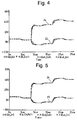
- Figure 4 is a graph showing the distorted voltage waveforms at the four corners of the display, both for the resultant 24 of the strobe and data waveforms and for the data waveform 25 alone, utilising SPICE modelling of such an addressable matrix array in which no current balancing is applied and in which the matrix consists of 12 rows and 38 columns with a row resistance of 0.1 ⁇ /sqr, a column resistance of 0.15 ⁇ /sqr, a column driver impedance of 300 ⁇ and a row driver impedance of 50 ⁇ . In this case no current balancing is applied by the addition of resistance values to the electrode tracks.
- Figure 5 shows the corresponding distorted voltage waveforms 24 and 25 for a similar model of a matrix array in which current balancing is applied by the application of varying resistance values to the coupling between the data signal generator 14 and the column electrode tracks 4 1 , 4 2 ... 4 n varying from 700 ⁇ to 300 ⁇ from the first column driver to the last column driver with the intermediate resistance values being evenly spread within the intervening range.
- a FLCD this results m more uniform optical properties across the display, as well as in more even temperature rises across the display.
- Such current balancing can be extended to the row electrode tracks so as to compensate for some of the waveform distortion introduced by the row electrode resistance.
- a resistance value of about 50 ⁇ (equivalent to the track length resistance) may be provided between the strobe signal generator 15 and the first row electrode track 5 1 whereas no additional resistance is applied between the generator 15 and the last row electrode track 5 m (with intermediate resistance values being applied to the intervening row electrode tracks S 2 ...S m-1 ).
- the general effect of current balancing is to match the best quality waveforms to the worst quality waveforms so that, although it reduces the spread of distortion, the current balancing may have the effect of moving the display operating point away from the ideal display operating point which would be obtained by use of undistorted switching waveforms.
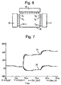
- FIG. 6 is a graph showing the voltage waveforms 24 and 25 at the four corner pixels (In,In), (In,Out), (Out,Out) and (Out, In) for such a matrix array in which alternate rows are driven from opposite ends, but in which no other current balancing measures are taken. It will be appreciated that, as compared with the graph of Figure 4, the spread of waveform distortion is reduced in a broadly similar manner to the current balancing arrangement previously described producing a reduction in the waveform distortion shown in Figure 5.
- the applied resistances of varying resistance values may be constituted by end portions of the column or row electrode tracks, or by further metalisation tracks electrically coupled to the end portions of the column or row electrode tracks.
- These additional resistance portions may be made to have different resistance values by being narrower than the rest of the track and by ensuring that each narrowed portion of different resistance value has a different width.
- each narrowed portion may be made to have a different resistance value by being of a different length.
- the narrowed portions of all the tracks may have the same width, and their resistance values may be varies simply by varying the length of the narrowed portion. The narrower the width the greater is the resistance value of the portion, and the greater the length of the narrowed portion the greater is its resistance value.
- the additional resistances may also simply be formed by conventional resistors having different resistance values.
Landscapes
- Engineering & Computer Science (AREA)
- Chemical & Material Sciences (AREA)
- Crystallography & Structural Chemistry (AREA)
- Physics & Mathematics (AREA)
- Computer Hardware Design (AREA)
- General Physics & Mathematics (AREA)
- Theoretical Computer Science (AREA)
- Liquid Crystal (AREA)
- Control Of Indicators Other Than Cathode Ray Tubes (AREA)
- Liquid Crystal Display Device Control (AREA)
- Devices For Indicating Variable Information By Combining Individual Elements (AREA)
Applications Claiming Priority (2)
| Application Number | Priority Date | Filing Date | Title |
|---|---|---|---|
| GB9902343 | 1999-02-04 | ||
| GBGB9902343.4A GB9902343D0 (en) | 1999-02-04 | 1999-02-04 | overnment Of The United Kingdom Of Great Britain And Northern Ireland The Addressable matrix arrays |
Publications (2)
| Publication Number | Publication Date |
|---|---|
| EP1026657A2 true EP1026657A2 (de) | 2000-08-09 |
| EP1026657A3 EP1026657A3 (de) | 2002-06-19 |
Family
ID=10847000
Family Applications (1)
| Application Number | Title | Priority Date | Filing Date |
|---|---|---|---|
| EP00300444A Withdrawn EP1026657A3 (de) | 1999-02-04 | 2000-01-21 | Adressierbare Matrixgeräte |
Country Status (3)
| Country | Link |
|---|---|
| EP (1) | EP1026657A3 (de) |
| JP (1) | JP2000227584A (de) |
| GB (1) | GB9902343D0 (de) |
Cited By (4)
| Publication number | Priority date | Publication date | Assignee | Title |
|---|---|---|---|---|
| US7019719B2 (en) | 2001-10-19 | 2006-03-28 | Clare Micronix Integrated Systems, Inc. | Method and clamping apparatus for securing a minimum reference voltage in a video display boost regulator |
| EP1221685A3 (de) * | 2000-12-22 | 2008-02-20 | Hitachi, Ltd. | Plasma-Anzeigegerät mit reduzierten Spannungseinbrüchen entlang leitender Linien |
| FR2916296A1 (fr) * | 2007-05-18 | 2008-11-21 | Nemoptic Sa | Procede d'adressage d'un ecran matriciel a cristal liquide et dispositif appliquant ce procede. |
| US8941640B2 (en) | 2012-06-08 | 2015-01-27 | Apple Inc. | Differential VCOM resistance or capacitance tuning for improved image quality |
Families Citing this family (1)
| Publication number | Priority date | Publication date | Assignee | Title |
|---|---|---|---|---|
| KR100840330B1 (ko) | 2002-08-07 | 2008-06-20 | 삼성전자주식회사 | 액정 표시 장치 및 이에 사용하는 구동 집적 회로 |
Family Cites Families (6)
| Publication number | Priority date | Publication date | Assignee | Title |
|---|---|---|---|---|
| FR2608300B1 (fr) * | 1986-12-16 | 1989-03-31 | Thomson Csf | Systeme de visualisation sur ecran plat matriciel avec affichage protege des donnees primordiales pour l'exploitation |
| JPH04269789A (ja) * | 1991-02-25 | 1992-09-25 | Seiko Instr Inc | 電気光学的表示装置 |
| JPH05203997A (ja) * | 1992-01-24 | 1993-08-13 | Toshiba Corp | 液晶表示装置 |
| JPH0777946A (ja) * | 1993-09-07 | 1995-03-20 | Seiko Epson Corp | 液晶表示装置 |
| KR960024595A (ko) * | 1994-12-29 | 1996-07-20 | 윤종용 | 강유전성 액정 표시 소자의 다계조 표시 장치 및 방법 |
| JPH11231287A (ja) * | 1998-02-19 | 1999-08-27 | Sharp Corp | 強誘電性液晶表示素子の駆動方法および駆動回路 |
-
1999
- 1999-02-04 GB GBGB9902343.4A patent/GB9902343D0/en not_active Ceased
-
2000
- 2000-01-21 EP EP00300444A patent/EP1026657A3/de not_active Withdrawn
- 2000-02-04 JP JP2000028402A patent/JP2000227584A/ja active Pending
Cited By (4)
| Publication number | Priority date | Publication date | Assignee | Title |
|---|---|---|---|---|
| EP1221685A3 (de) * | 2000-12-22 | 2008-02-20 | Hitachi, Ltd. | Plasma-Anzeigegerät mit reduzierten Spannungseinbrüchen entlang leitender Linien |
| US7019719B2 (en) | 2001-10-19 | 2006-03-28 | Clare Micronix Integrated Systems, Inc. | Method and clamping apparatus for securing a minimum reference voltage in a video display boost regulator |
| FR2916296A1 (fr) * | 2007-05-18 | 2008-11-21 | Nemoptic Sa | Procede d'adressage d'un ecran matriciel a cristal liquide et dispositif appliquant ce procede. |
| US8941640B2 (en) | 2012-06-08 | 2015-01-27 | Apple Inc. | Differential VCOM resistance or capacitance tuning for improved image quality |
Also Published As
| Publication number | Publication date |
|---|---|
| JP2000227584A (ja) | 2000-08-15 |
| GB9902343D0 (en) | 1999-03-24 |
| EP1026657A3 (de) | 2002-06-19 |
Similar Documents
| Publication | Publication Date | Title |
|---|---|---|
| EP0592201B1 (de) | Adaptive Steuerungswellenformen zur Verringerung des Übersprechens in elektrooptischer Adressierungsstruktur | |
| US4062626A (en) | Liquid crystal display device | |
| KR100269849B1 (ko) | 액티브매트릭스형 액정표시장치(active matrix type liquid crystal display device) | |
| JPH11344961A5 (de) | ||
| EP0691639B1 (de) | Verfahren und Einrichtung zur Steuerung einer ferroelektrischen Flüssigkristallanzeigetafel | |
| KR100633812B1 (ko) | 광변조 장치 | |
| JP3141312B2 (ja) | 表示素子 | |
| JP2847666B2 (ja) | 電気光学表示方法 | |
| US5220315A (en) | Power source for dot matrix lcd | |
| EP1026657A2 (de) | Adressierbare Matrixgeräte | |
| EP0823067B1 (de) | Elektrooptische anzeigevorrichtungen | |
| EP0807845B1 (de) | Adressierbare Matrix zur Ansteurung eines Bildschirms | |
| EP0685832B1 (de) | Ferroelektrische Flüssigkristallanzeigevorrichtung und Ansteuerungsverfahren zur Durchführung einer abgestufften Anzeige | |
| US5940060A (en) | Ferroelectric liquid crystal cell, method of controlling such a cell, and display | |
| US6215533B1 (en) | Ferroelectric liquid crystal driving using square wave and non-square wave signals | |
| KR100324438B1 (ko) | 액정 디바이스 및 액정 디바이스의 어드레스 방법 | |
| KR100279684B1 (ko) | 액정 디바이스 및 액정 디바이스를 어드레싱하는 방법 | |
| JPH08304772A (ja) | 強誘電性液晶表示パネルの駆動方法 | |
| KR100326453B1 (ko) | 강유전성액정표시장치의구동방법 | |
| JP2630027B2 (ja) | 液晶パネル及びその製造法 | |
| KR100280698B1 (ko) | 액티브 어드레싱 액정표시장치의 구동방법 | |
| JP2805252B2 (ja) | 液晶装置 | |
| JPH1054976A (ja) | 液晶表示装置ならびにその駆動回路および駆動方法 | |
| JPH0618853A (ja) | 表示装置 | |
| JPH07181445A (ja) | 液晶表示装置 |
Legal Events
| Date | Code | Title | Description |
|---|---|---|---|
| PUAI | Public reference made under article 153(3) epc to a published international application that has entered the european phase |
Free format text: ORIGINAL CODE: 0009012 |
|
| AK | Designated contracting states |
Kind code of ref document: A2 Designated state(s): AT BE CH CY DE DK ES FI FR GB GR IE IT LI LU MC NL PT SE |
|
| AX | Request for extension of the european patent |
Free format text: AL;LT;LV;MK;RO;SI |
|
| PUAL | Search report despatched |
Free format text: ORIGINAL CODE: 0009013 |
|
| AK | Designated contracting states |
Kind code of ref document: A3 Designated state(s): AT BE CH CY DE DK ES FI FR GB GR IE IT LI LU MC NL PT SE |
|
| AX | Request for extension of the european patent |
Free format text: AL;LT;LV;MK;RO;SI |
|
| 17P | Request for examination filed |
Effective date: 20021219 |
|
| AKX | Designation fees paid |
Designated state(s): DE FR GB |
|
| 17Q | First examination report despatched |
Effective date: 20030304 |
|
| RAP1 | Party data changed (applicant data changed or rights of an application transferred) |
Owner name: SHARP KABUSHIKI KAISHA Owner name: QINETIQ LIMITED |
|
| STAA | Information on the status of an ep patent application or granted ep patent |
Free format text: STATUS: THE APPLICATION IS DEEMED TO BE WITHDRAWN |
|
| 18D | Application deemed to be withdrawn |
Effective date: 20040803 |