EP1030486A2 - Circuit d'attaque et module pour transmission optique - Google Patents
Circuit d'attaque et module pour transmission optique Download PDFInfo
- Publication number
- EP1030486A2 EP1030486A2 EP99307397A EP99307397A EP1030486A2 EP 1030486 A2 EP1030486 A2 EP 1030486A2 EP 99307397 A EP99307397 A EP 99307397A EP 99307397 A EP99307397 A EP 99307397A EP 1030486 A2 EP1030486 A2 EP 1030486A2
- Authority
- EP
- European Patent Office
- Prior art keywords
- transistors
- driver circuit
- optical
- circuit
- base
- Prior art date
- Legal status (The legal status is an assumption and is not a legal conclusion. Google has not performed a legal analysis and makes no representation as to the accuracy of the status listed.)
- Granted
Links
- 230000003287 optical effect Effects 0.000 title claims description 49
- 230000005540 biological transmission Effects 0.000 title description 7
- 238000012544 monitoring process Methods 0.000 claims 4
- 238000010586 diagram Methods 0.000 description 27
- 229910001218 Gallium arsenide Inorganic materials 0.000 description 7
- 239000000463 material Substances 0.000 description 6
- 230000000694 effects Effects 0.000 description 5
- 238000000034 method Methods 0.000 description 5
- 238000010521 absorption reaction Methods 0.000 description 3
- 230000000295 complement effect Effects 0.000 description 3
- 238000013016 damping Methods 0.000 description 3
- 230000003071 parasitic effect Effects 0.000 description 3
- 229920006395 saturated elastomer Polymers 0.000 description 3
- VYPSYNLAJGMNEJ-UHFFFAOYSA-N Silicium dioxide Chemical compound O=[Si]=O VYPSYNLAJGMNEJ-UHFFFAOYSA-N 0.000 description 2
- 230000002411 adverse Effects 0.000 description 2
- 230000002238 attenuated effect Effects 0.000 description 1
- 229910052681 coesite Inorganic materials 0.000 description 1
- 238000004891 communication Methods 0.000 description 1
- 229910052906 cristobalite Inorganic materials 0.000 description 1
- 230000003247 decreasing effect Effects 0.000 description 1
- 238000001514 detection method Methods 0.000 description 1
- 238000005516 engineering process Methods 0.000 description 1
- 230000005669 field effect Effects 0.000 description 1
- 238000005259 measurement Methods 0.000 description 1
- 239000013307 optical fiber Substances 0.000 description 1
- 230000010287 polarization Effects 0.000 description 1
- 238000012545 processing Methods 0.000 description 1
- 238000011160 research Methods 0.000 description 1
- 239000000523 sample Substances 0.000 description 1
- 239000000377 silicon dioxide Substances 0.000 description 1
- 235000012239 silicon dioxide Nutrition 0.000 description 1
- 230000000087 stabilizing effect Effects 0.000 description 1
- 229910052682 stishovite Inorganic materials 0.000 description 1
- 239000000758 substrate Substances 0.000 description 1
- 229910052905 tridymite Inorganic materials 0.000 description 1
Images


Classifications
-
- H—ELECTRICITY
- H04—ELECTRIC COMMUNICATION TECHNIQUE
- H04L—TRANSMISSION OF DIGITAL INFORMATION, e.g. TELEGRAPHIC COMMUNICATION
- H04L25/00—Baseband systems
- H04L25/02—Details ; arrangements for supplying electrical power along data transmission lines
- H04L25/0264—Arrangements for coupling to transmission lines
- H04L25/028—Arrangements specific to the transmitter end
- H04L25/0282—Provision for current-mode coupling
-
- H—ELECTRICITY
- H04—ELECTRIC COMMUNICATION TECHNIQUE
- H04B—TRANSMISSION
- H04B10/00—Transmission systems employing electromagnetic waves other than radio-waves, e.g. infrared, visible or ultraviolet light, or employing corpuscular radiation, e.g. quantum communication
- H04B10/50—Transmitters
- H04B10/501—Structural aspects
- H04B10/503—Laser transmitters
- H04B10/504—Laser transmitters using direct modulation
-
- H—ELECTRICITY
- H04—ELECTRIC COMMUNICATION TECHNIQUE
- H04B—TRANSMISSION
- H04B10/00—Transmission systems employing electromagnetic waves other than radio-waves, e.g. infrared, visible or ultraviolet light, or employing corpuscular radiation, e.g. quantum communication
- H04B10/50—Transmitters
- H04B10/564—Power control
Definitions
- the present invention relates to a driver circuit capable of generating an output with a large amplitude from a low power-supply voltage, and also relates to an optical-transmission module employing the driver circuit stated above.
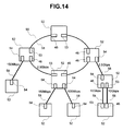
- Fig. 14 shows an example of an optical network studied by the inventors in developing the present invention.
- the optical network of Fig. 14 uses various optical fibers which send signals at different signal speeds such as 50Mbps, 600Mbps, 2.5Gbps and lOGbps.
- Devices 52 such as transmitting devices and routers employed in the optical network have optical transmitting modules 46, optical receiving modules 53, and optical modules 54 which effectively combine the optical transmitting modules 46 and the optical receiving modules 53, which modules handle signals at their different signal speed.
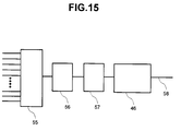
- the optical transmitting modules 46 can be electrically connected to logic circuits such as a MUX circuit 55 for making low-speed signals time division multiplexed, a header adding circuit 56 for inserting a header, which includes necessary information for the network such as information for error detection, to data, and a scrambling circuit 57 for protecting data from continuing the same data "0" or "1" for a long period of time.
- the logic circuit such as the MUX circuit 55, the header adding circuit 56, and the scrambling circuit 57 are applied with a low power-supply voltage such as 5 V or -5.2 3.3 V for making them low power consumption devices.
- a driver circuit employing an optical transmitting module 46 for transmitting signals at low speed less than 600Mbps comprises a changeable-current supply and current mirror circuit. And it can work with a low power-supply voltage of 3.3 V.
- Such circuits are described in the MAXIM company catalog MAX3667 and are especially shown in Fig. 1 of page 6 of this catalog.
- a driver circuit employing an optical transmitting module such as module 46 for transmitting signals at high speed more than 2.5Gbps is fabricated by adopting a GaAs process to increase the processing speed of the driver circuit.
- the driver circuit employs a pair of transistors with the emitters thereof connected to each other to function as a differential-amplifier circuit and a constant-current supply circuit connected to the emitter connection point of the pair of transistors.
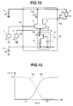
- Such a driver circuit 10 is shown in Fig. 12.
- the driver circuit 10 comprises a pair of transistors 11 and 12 forming a differential-amplifier circuit.
- the transistors 11 and 12 are each a FET (field effect transistor) made of GaAs.
- the emitters of the transistors are connected to each other.
- a constant-current supply circuit 13 is provided between the emitter connection point of the transistors 11 and 12 and a power supply 8.
- the constant-current supply circuit 13 comprises a transistor 15, a resistor 16 and a voltage supply 14.
- the driver circuit 10 drives a load 2.
- the driver circuit which comprises a changeable-current supply and a current returning circuit needs a complementary bipolar process for making PNP transistor as a vertical structure and NPN transistor as a vertical structure on the same chip. Therefore, since it make the chip structure complicated, the performance of the transistor is inferior to a transistor made by a bipolar process, not a complementary bipolar process. Therefore, this driver circuit can't employ the optical transmitting module for transmitting signals at high speed.
- the GaAs FETs employed in the driver circuit which has the optical transmitting module for transmitting signals at high speed are expensive in comparison with a bipolar transistor made of a material such as Si.
- a bipolar transistor made of a material such as Si By merely replacing the pair of FETs employed in the related art driver circuit with low-cost bipolar transistors made of a material such as Si, however, it is difficult to operate the driver circuit without causing the bipolar transistors to enter a saturated state at a low power-supply voltage such as 3.3 V since a voltage in the range of 0.7V to 0.8V is required between the base and the emitter of each of the transistors.
- the device size since two power supplies are needed, one power supply for the logic circuit and the optical module for transmitting signals at low speed less than 600Mbps and another power supply for the optical module for transmitting signals at high speed more than 2.5Gbps, the device size become large.
- a driver circuit comprising a first differential-amplifier circuit having a pair of first transistors with emitters thereof connected to each other and a first resistor provided between an emitter connection point of the first transistors and first power supply.
- a difference in electric potential is applied between bases of the pair of the first transistors to set a ratio of a current flowing through one of the pair of the first transistors to a current flowing through the other first transistor at about 1/100 or smaller, and an amplitude of an output current is controlled by a higher electric potential applied to the base of one of the first transistors.
- Another driver circuit in accordance with the present invention comprises a first differential-amplifier circuit composed of a pair of first transistors employing bipolar transistors with emitters thereof connected to each other and a first resistor with resistance in the range of about 2 to 20 provided between an emitter connection point of the pair of the first transistors and a first power supply, wherein an amplitude of an output current is controlled by electric potential applied to a base of the first transistor.
- An optical-transmission module in accordance with the present invention comprises a driver circuit having a first differential-amplifier circuit, the first differential-amplifier circuit having a pair of first transistors with emitters thereof connected to each other and a first resistor provided between an emitter connection point of the first transistors and a first power supply, with a difference in electric potential applied between bases of the pair of the first transistors to set a ratio of a current flowing through one of the pair of the first transistors to a current flowing through the other first transistor at about 1/100 or smaller, and a laser-diode module for outputting an optical-transmission wave by carrying out optical-intensity modulation on a laser diode on a basis of an output current signal or an output voltage signal output by the first differential-amplifier circuit, wherein an output current of the driver circuit is controlled by a higher electric potential applied to the base of one of the first transistors.
- Another optical-transmission module in accordance with the present invention comprises a driver circuit having a first differential-amplifier circuit, the first differential-amplifier circuit having a pair of first transistors with emitters thereof connected to each other and a first resistor with resistance in the range of about 2 to 20 provided between an emitter connection point of the pair of the first transistors and a first power supply, and a laser-diode module for outputting an optical-transmission wave by carrying out optical-intensity modulation on a laser diode on a basis of an output current signal or an output voltage signal output by the first differential-amplifier circuit, wherein an output current of the driver circuit is controlled by electric potential applied to a base of the first transistor.
- Another optical-transmission module in accordance with the present invention comprises a driver circuit having a first differential-amplifier circuit, the first differential-amplifier circuit having a pair of first transistors with emitters thereof connected to each other and a first resistor provided between an emitter connection point of the first transistors and a first power supply, with a difference in electric potential applied between bases of the pair of the first transistors to set a ratio of a current flowing through one of the pair of the first transistors to a current flowing through the other first transistor at about 1/100 or smaller, and a optical-modulation module for outputting an optical-transmission wave by modulating a light emitted by a light source on the basis of an output current signal or an output voltage signal output by said first differential-amplifier circuit, wherein an output current of the driver circuit is controlled by a higher electric potential applied to the base of one of the first transistors.
- Another optical-transmission module in accordance with the present invention comprises a driver circuit having a first differential-amplifier circuit, the first differential-amplifier circuit having a pair of first transistors with emitters thereof connected to each other and a first resistor with resistance in the range of about 2 to 20 provided between an emitter connection point of the pair of the first transistors and a first power supply, and a optical-modulation module for outputting an optical-transmission wave by modulating a light emitted by a light source on the basis of an output current signal or an output voltage signal output by said first differential-amplifier circuit, wherein an output current of the driver circuit is controlled by electric potential applied to a base of the first transistor.
- Another driver circuit in accordance with the present invention comprises a differential-amplifier circuit having a pair of transistors, means for setting a ratio of a current flowing through one of a pair of transistors to a current flowing through the other transistor at about 1/100 or smaller, and means for controlling the amplitude of an output current by the higher electric potential applied to said base of one of said transistors.
- Another optical-transmission module in accordance with the present invention comprises a first optical module to transmit signals at low speed, a second optical module to transmit signals at high speed, and a power supply to supply substantially the same power supply voltage to both the first optical module and the second optical module.
- Another optical-transmission module in accordance with the present invention comprises a driver circuit having a differential-amplifier circuit with a pair of transistors and means for setting a ratio of a current flowing through one of a pair of transistors to a current flowing through the other transistor at about 1/100 or smaller and means for controlling the amplitude of an output current by the higher electric potential applied to said base of one of said transistors, and a optical-modulation module for outputting an optical-transmission wave by modulating a light emitted by a light source on the basis of an output current signal or an output voltage signal output by said differential-amplifier circuit, wherein an output current of the driver circuit is controlled by electric potential applied to a base of the transistor.
- the amplitude of an output can be increased by a difference in voltage between the base and the emitter of a transistor.
- bipolar transistors made of a low-cost material such as Si
- a driver circuit having the amplitude of an output signal at least equal to that of a driver circuit having a differential-amplifier circuit employing a pair of FETs each made of GaAs and the related art constant-current supply employing a pair of FETs each made of GaAs and the related art constant-current supply.
- optical-transmission modules having configurations described above, it is possible to transmit data by driving a laser diode or an optical modulator by means of the low-cost driver circuit described above to generate an optical-transmission wave with an improved quality.
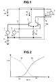
- Fig. 1 is a circuit diagram showing the first embodiment of the present invention implementing a driver circuit.
- the driver circuit 1Da comprises a pair of bipolar transistors 3 and 4 with their emitters connected to each other to form a differential-amplifier circuit.
- a resistor 5 having a resistance in the range of about 2 to 20 is provided between the emitter connection point of the transistors 3 and 4 and a power supply 8.
- the driver circuit 1Da drives a load 2.
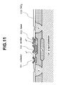
- the each of the transistors 3 and 4 is an NPN bipolar transistor which is made of a low-cost material such as Si and has a typical structure shown in Fig. 11.
- an NPN bipolar transistor comprises a p layer, an n layer and an embedded n+ layer which are provided on a p-type substrate 134.
- the NPN bipolar transistor also has a p layer connected to a base 113, an n+ layer connected to an emitter 112 and an n+ layer connected to a collector 111.
- a high voltage in the range of 0.7V to 0.8V is required to apply between the base 113 and the emitter 112.
- reference numeral 110 denotes an oxide film made of SiO2.
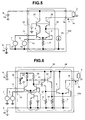
- Fig. 2 is a diagram showing input/output characteristics of the driver circuit 1Da.
- the solid line represents an output current 1a of the driver circuit 1Da which is denoted by a symbol I1.
- the dotted line represents a collector current 4a of the transistor 4 which is denoted by a symbol I4.
- the output current 1a of the driver circuit 1Da which is denoted by a symbol I1 increases as a voltage difference (V6-V7) rises where the symbol V6 denotes an input voltage 6 and the symbol V7 denotes an input voltage 7.
- V6-V7 For a voltage difference (V6-V7) between V6 denoting the input voltage 6 and V7 denoting the input voltage 7 equal to or greater than Vb, the value I1 of the output current 1a is given by Eq. (1) shown below.
- Vb is a level of the voltage difference (V6-V7) at which the collector current 4a of the transistor 4 becomes equal to about 1/100 or less of the collector current 1a of the transistor 3.
- the amplitude of the current I1 of the driver circuit 1Da is determined by the higher one of the base electric potentials V6 and V7 of the transistors 3 and 4, respectively at a level of the voltage difference (V6-V7) at which the current flowing to one of the transistors 3 and 4 becomes equal to about 1/100 or less of the current flowing to the other transistor.
- the amplitude of the output current I1 provided by the collector of the transistor 3 is controlled by the base electric potential V6 of the transistor 3 which is higher than the base electric potential V7 of the transistor 4 at a level of the voltage difference (V6-V7) at which the current I4 flowing to the transistor 4 becomes equal to about 1/100 or less of the current I1 flowing to the other transistor I3.
- Fig. 13 is a diagram showing input/output characteristics of the related art driver circuit 10.
- the solid line represents an output current 10a of the driver circuit 10 which is denoted by a symbol I10.
- the dotted line represents a collector current 12a of the transistor 12 which is denoted by a symbol I12.
- the output current 10a of the driver circuit 10 which is denoted by a symbol I10 increases as a voltage difference (V6-V7) rises where the symbol V6 denotes an input voltage 6 and the symbol V7 denotes an input voltage 7.
- V6-V7 For a voltage difference (V6-V7) between V6 denoting the input voltage 6 and V7 denoting the input voltage 7 equal to or greater than Vb, the current value I10 of the output current 10a becomes about equal to a value I13 of a current 13a output by the constant-current supply circuit 13.
- Vb is a level of the voltage difference (V6-V7) at which the collector current 12a of the transistor 12 becomes equal to about 1/100 or less of the collector current 10a of the transistor 11.
- the amplitude of the current output by the driver circuit 10 is determined by the current value I13 of the current 13a output by the constant-current supply circuit 13 and controlled by changing the voltage generated by the voltage supply 14 at a level of the voltage difference (V6-V7) at which the current flowing to one of the pair of transistors 11 and 12 becomes equal to about 1/100 or less of the current flowing to the other transistor.
- the characteristic of the driver circuit 1Da provided by the present invention as shown in Fig. 1 can be described as below in comparison with the characteristics of the related art driver circuit 10 shown in Fig. 12.
- the symbol Vbe3 denotes a voltage between the base and the emitter of the transistor 3
- the symbol Z2 denotes the impedance of the load 2
- R5 denotes the resistance of the resistor 5.
- the symbol Vbe11 denotes a voltage between the base and the emitter of the GaAs FET 11
- the symbol Vbe15 denotes a voltage between the base and the emitter of the GaAs FET 15
- the symbol Z2 denotes the impedance of the load 2
- R16 denotes the resistance of the resistor 16.
- a resistor may be connected between the collector of the transistor 4 and the power supply 9.
- NPN transistors are employed in the driver circuit 1Da shown in Fig. 1 as the transistors 3 and 4, PNP transistors may also be used.
- the characteristics shown in Fig. 2 can be obtained.
- the characteristics indicate that a large output current I1 can be generated in comparison with the ordinary differential amplifier (or the driver circuit) 10 of Fig. 12 having the same power-supply voltages V9 and V8.
- the same output current I1 in comparison with the ordinary differential amplifier (or the driver circuit) 10 of Fig. 12 can be generated with lower power-supply voltages V9 and V8 than the ordinary differential amplifier (or the driver circuit) 10 of Fig. 12.
- driver circuit 1Da shown in Fig. 1 is applied to an optical-transmission module employing an LD (laser diode) as will be described later, an operation in a higher ambient temperature range is possible since a larger current can be flowed to the LD. That is to say, at a high temperature, it is necessary to flow a larger current into the LD for generating a larger optical output.
- LD laser diode
- a damping resistor 48 having a higher resistance can be connected between the driver 1Da and the LD to generate the same current. As a result, the quality of the optical-transmission wave can be improved.
- the driver circuit 1Da shown in Fig. 1 is applied to an optical-transmission module employing an LD (laser diode) as will be described later, the power supply voltage of the driver circuit 1Da can be reduce to generate the same current when the same damping resistor 48 is used. As a result, the power supply voltage of the optical module can be reduced.
- LD laser diode
- Fig. 3 is a circuit diagram showing the second embodiment implementing the driver circuit provided by the present invention.
- the driver circuit 1Db comprises a pair of bipolar transistors 3 and 4 described above with their emitters connected to each other to form a differential-amplifier circuit. Resistors 17 and 18 are connected to the collectors of the transistors 3 and 4 respectively. A resistor 5 having a lowered resistance in the range of about 2 to 20 is provided between the emitter connection point of the transistors 3 and 4 and a power supply 8.
- the driver circuit 1Db drives a load 2.
- the resistance of the resistor 17 By setting the resistance of the resistor 17 at a value equal to the characteristic impedance Z0 of a transmission line 19 connecting the driver circuit 1Db to the load 2, it is possible to reduce the number of multiple reflections occurring between the driver circuit 1Db and the load 2, and hence to improve the quality of the optical-transmission waveform.
- the resistor 17 By connecting the resistor 17 between the collector of the transistor 3 and the power supply 9, it is possible to control the amplitude of a voltage output from the collector of the transistor 3 by the electric potential V6 at the base of the transistor 3 which is higher than that of the transistor 4.
- resistor 18 is connected to the transistor 4 as shown in Fig. 3, the resistor 18 can be omitted.
- NPN transistors are employed in the driver circuit 1Db shown in Fig. 3 as the transistors 3 and 4, PNP transistors may also be used.
- the characteristics shown in Fig. 2 can be obtained.
- the characteristics indicate that a large output current I1 can be generated in comparison with the ordinary differential amplifier (or the driver circuit) 10 of Fig. 12 when having the same power-supply voltages V9 and V8.
- driver circuit 1Db when the driver circuit 1Db is applied to an optical-transmission module employing an LD (laser diode) as will be described later, the same effect as the driver circuit 1Da can be obtained.
- LD laser diode
- driver circuit 1Db when the driver circuit 1Db is applied to an optical-transmission module employing an EA (electrical absorption), a larger modulation voltage can be setted. As a result, optical characteristics can be improved.
- EA electrical absorption
- the driver circuit 1Db when the driver circuit 1Db is applied to an optical-transmission module employing an EA (electrical absorption), the power supply voltage of the driver circuit can be reduced to generate the same modulation voltage. As a result, the power supply voltage of the optical module can be reduced.
- EA electric absorption
- Fig. 4 is a circuit diagram showing the third embodiment implementing the driver circuit provided by the present invention.
- the driver circuit 1Dc comprises a pair of bipolar transistors 3 and 4 described above with their emitters connected to each other to form a differential-amplifier circuit.
- a transistor 20 forming a grounded-base circuit is connected to the collector of the transistor 3.
- a transistor 21 forming a grounded-base circuit is connected to the collector of the transistor 4.
- a resistor 5 having a lowered resistance in the range of about 2 to 20 is provided between the emitter connection point of the transistors 3 and 4 and a power supply 8.
- the driver circuit 1Dc drives a load 2.
- the transistor 20 forming a grounded-base circuit reduces a mirror capacitance which occurres between the base and the collector of the transistor 3.
- the transistor 21 forming a grounded-base circuit reduces a mirror capacitance between the base and the collector of the transistor 4. As a result, the speed of the driver circuit 1Dc is increased.
- collector of the transistor 21 is connected directly to the power supply 9 as shown in Fig. 4, the collector of the transistor 21 can also be connected by a resistor to the power supply 9.
- the collector of the transistor 20 can also be connected by a resistor to the power supply 9 in the driver circuit 1Dc to provide a driver circuit similar to that shown in Fig. 3.
- the resistance of the resistor connected between the collector of the transistor 20 and the power supply 9 at a value equal to the characteristic impedance Z0 of a transmission line 19 connecting the driver circuit 1Dc to the load 2, it is possible to reduce the number of multiple reflections occurring between the driver circuit 1Dc and the load 2, and hence to improve the quality of the waveform.
- NPN transistors are employed in the driver circuit 1Dc shown in Fig. 4 as the transistors 3 and 4, PNP transistors may also be used.
- the driver circuit 1Dc allows the characteristics shown in Fig. 2 to be obtained.
- the characteristics indicate that a large output current I1 and output voltage can be generated in comparison with the ordinary differential amplifier (or the driver circuit) 10 of Fig. 12 when having the same power-supply voltages V9 and V8.
- driver circuit 1Dc when the driver circuit 1Dc is applied to an optical-transmission module employing an LD (laser diode) as will be described later, the same effect as the driver circuits 1Da and 1Db can be obtained. Further, a much higher transmission speed can be implemented.
- LD laser diode
- Fig. 5 is a circuit diagram showing the fourth embodiment implementing the driver circuit provided by the present invention.
- the driver circuit 1Dd comprises a pair of bipolar transistors 3 and 4 described above with their emitters connected to each other to form a differential-amplifier circuit.
- a transistor 20 forming a grounded-base circuit is connected to the collector of the transistor 3.
- a transistor 21 forming a grounded-base circuit is connected to the collector of the transistor 4.
- a resistor 5 having a resistance in the range of about 2 to 20 is provided between the emitter connection point of the transistors 3 and 4 and a power supply 8.
- the driver circuit 1Dd also includes a constant-current supply circuit 23 connected to a connection point between the emitter of the transistor 20 forming a grounded-base circuit and the collector of the transistor 3 in the transistor pair.
- the driver circuit 1Dd drives a load 2.
- the driver circuit 1Dd is capable of providing an offset current to the load 2.
- collector of the transistor 21 is connected directly to the power supply 9 as shown in Fig. 5, the collector of the transistor 21 can also be connected by a resistor to the power supply 9.
- the collector of the transistor 20 can also be connected by a resistor to the power supply 9 as is the case with the driver circuit 1Db shown in Fig. 3.
- the resistance of this resistor at a value equal to the characteristic impedance Z0 of a transmission line 19 connecting the driver circuit 1Dd to the load 2, it is possible to reduce the number of multiple reflections occurring between the driver circuit 1Dd and the load 2 and, hence, to improve the quality of the waveform.
- a constant-current supply circuit similar to the constant-current supply circuit 23 can also be connected to the transistor 4.
- NPN transistors are employed in the driver circuit 1Dd shown in Fig. 5 as the transistors 3 and 4, PNP transistors may also be used.
- the driver circuit 1Dd explained above allows a bias current or a bias voltage to be applied to the load 2.
- the bias (constant-current supply) circuit 23 to an emitter of the grounded-base circuit composing the transistors 20 and 21 and a power supply 22, it is possible to reduce an effect of a parasitic capacitance of the bias circuit on the operating speed of the driver circuit 1Dd.
- driver circuit 1Dd to an optical-transmission module adopting EA (electronic absorption), it is possible to apply more modulation voltages and more bias voltages, and hence to improve the optical characteristics.
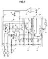
- Fig. 6 is a circuit diagram showing the fifth embodiment implementing the driver circuit provided by the present invention.
- the driver circuit 1De comprises a differential-amplifier circuit 24 and a preamplifier circuit 35, driving a load 2.
- the differential-amplifier circuit 24 comprises a pair of bipolar transistors 3 and 4 with their emitters connected to each other, and a resistor 5 provided between the emitter connection point of the transistors 3 and 4 and a power supply 8.
- the preamplifier circuit 35 comprises a differential-amplifier circuit and two emitter-follower circuits.
- the differential-amplifier circuit comprises a pair of bipolar transistors 25 and 26 with their emitters connected to each other, a constant-current supply circuit 27 provided between the emitter connection point of the transistors 25 and 26 and the power supply 8, a resistor 28 connected to the collector of the transistor 25, a resistor 29 connected to the collector of the transistor 26 and a variable power supply 30 connected to the other ends of the resistors 28 and 29.
- One of the emitter-follower circuits comprises a transistor 31 with the base thereof connected to the collector of the transistor 25 and a resistor 32 connected to the emitter of the transistor 31 whereas the other emitter-follower circuit comprises a transistor 33 with the base thereof connected to the collector of the transistor 26 and a resistor 34 connected to the emitter of the transistor 33.
- the emitter of the transistor 31 is connected to the base of the transistor 4 employed in the differential-amplifier circuit 24 while the emitter of the transistor 33 is connected to the base of the transistor 3 employed in the differential-amplifier circuit 24.
- the preamplifier circuit 35 allows the input voltages 6 and 7 of the driver circuit 1De to be kept at fixed values without regard to the amplitude of the current la output by the driver circuit 1De.
- differential-amplifier circuit 24 is not limited to the configuration shown in Fig. 6, but can also be implemented by the differential-amplifier circuits shown in Figs. 3 to 5.
- the resistor 32 employed in one of the emitter-follower circuits of the preamplifier circuit 35 besides the transistor 31 can be replaced by a constant-current supply circuit.
- the resistor 34 employed the other emitter-follower circuit of the preamplifier circuit 35 besides the transistor 33 can be replaced by a constant-current supply circuit.
- NPN transistors are employed in the driver circuit 1De shown in Fig. 6, PNP transistors may also be used.
- the preamplifier circuit 35 allows the input voltages to be kept at fixed values.
- an output voltage of an ordinary digital IC which can not be changed can be applied to the driver circuit (driver IC) 1De as an input.
- an ordinary digital IC outputs predetermined high and low voltages which cannot be changed.
- the values of the output current and the output voltage of the driver circuit 1De can be changed all but proportionally to a voltage generated by the variable voltage supply 30. That is to say, control is easy to execute since there is no abrupt-change point.
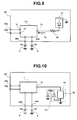
- Fig. 7 is a circuit diagram showing the sixth embodiment implementing the driver circuit provided by the present invention.
- the driver circuit 1Df comprises a differential-amplifier circuit 24, a preamplifier circuit 35 and a monitor circuit 42 for driving a load 2.
- the differential-amplifier circuit 24 comprises a pair of bipolar transistors 3 and 4 with their emitters connected to each other, and a resistor 5 provided between the emitter connection point of the transistors 3 and 4 and a power supply 8.
- the preamplifier circuit 35 comprises a differential-amplifier circuit and two emitter-follower circuits.
- the differential-amplifier circuit comprises a pair of bipolar transistors 25 and 26 with their emitters connected to each other, a constant-current supply circuit 27 provided between the emitter connection point of the transistors 25 and 26 and the power supply 8, a resistor 28 connected to the collector of the transistor 25, a resistor 29 connected to the collector of the transistor 26 and a variable power supply 30 connected to the other ends of the resistors 28 and 29.
- One of the emitter-follower circuit comprises a transistor 31 with the base thereof connected to the collector of the transistor 25 and a resistor 32 connected to the emitter of the transistor 31 whereas the other emitter-follower circuit comprises a transistor 33 with the base thereof connected to the collector of the transistor 26 and a resistor 34 connected to the emitter of the transistor 33.
- the emitter of the transistor 31 is connected to the base of the transistor 4 employed in the differential-amplifier circuit 24 while the emitter of the transistor 33 is connected to the base of the transistor 3 employed in the differential-amplifier circuit 24.
- the monitor circuit 42 comprises an emitter-follower circuit, a transistor 39 and resistors 40 and 41.
- the emitter-follower circuit comprises resistors 36 and 38, and a transistor 37.
- the resistor 36 is connected to the variable voltage supply 30 and has a resistance N times that of the resistor 29.
- the other end of the resistor 36 is connected to the base of the transistor 37 which has an emitter area 1/N times that of the transistor 33.
- the resistor 38 Connected between the power supply 8 and the emitter of the transistor 37, the resistor 38 has a resistance N times that of the resistor 34.
- the output of the emitter-follower circuit is connected to the base of the transistor 39 which has an emitter area 1/N times that of the transistor 3.
- the resistor 40 Connected between the power supply 8 and the emitter of the transistor 39, the resistor 40 has a resistance N times that of the resistor 5 which has a lowered resistance in the range of about 2 to 20.
- the resistor 41 is connected between the collector of the transistor 39 and the power supply 9.
- the amplitude of the collector current of the transistor 39 employed in the monitor circuit 42 becomes equal to 1/N times that of the current 1a output by the driver circuit 1Df.
- the voltage V1m appearing at an amplitude monitor terminal 1e of the driver circuit 1Df can thus be treated as a monitored voltage representing the amplitude of the current 1a output by the driver circuit 1Df.
- V1m R41 I1m / N * (5) where the symbol R41 denotes the resistance of the resistor 41 and the symbol I1m denotes the amplitude of the current 1a output by the driver circuit 1Df.
- the difference between the voltage appearing at the amplitude monitor terminal le of the driver circuit 1Df and the stable voltage of a voltage supply 44 is amplified by a differential amplifier 43 to produce an output for controlling the voltage generated by the variable voltage supply 30 employed in the preamplifier circuit 35 of the driver circuit 1Df.
- the amplitude of the current 1a output by the driver circuit 1Df can be stabilized.
- differential-amplifier circuit 24 is not limited to the configuration shown in Fig. 7, but can also be implemented by the differential-amplifier circuits shown in Figs. 3 to 5.
- the resistor 32 employed in one of the emitter-follower circuits of the preamplifier circuit 35 besides the transistor 31 can be replaced by a constant-current supply circuit.
- the resistor 34 employed the other emitter-follower circuit of the preamplifier circuit 35 besides the transistor 33 can be replaced by a constant-current supply circuit.
- NPN transistors are employed in the driver circuit 1Df shown in Fig. 7, PNP transistors may also be used.
- the monitor circuit 42 employed in the driver circuit 1Df allows the current and voltage output by the driver circuit 1Df to be known without adversely affecting an output circuit.
- a probe or an input terminal of a measurement apparatus can also be brought into electrical contact with the output of the driver circuit 1Df outputting a waveform which changes at a high speed. In this case, however, the quality of the waveform will deteriorate, adversely affecting the output circuit.
- the voltage output by the monitor circuit 42 is supplied to a circuit comprising the operational amplifier 43 and the voltage supply 44 to make the current and voltage output by the driver circuit 1Df more precise and more stable.
- the voltage output by the monitor circuit 42 can be increased to a level in the range of 2 to 3V in the case of the driver circuit lDf
- the voltage generated by the voltage supply 44 can also be increased to a level in the range of 2 to 3V as well.
- the circuit comprising the operational amplifier 43 and the voltage supply 44 is hardly affected by noise.
- a D/A (digital to analog) converter can be directly connected, the need for an amplifier circuit can be eliminated.
- Fig. 8 is a circuit diagram showing the seventh embodiment implementing the driver circuit provided by the present invention.
- the driver circuit 1Dg comprises a differential-amplifier circuit 24 and a preamplifier circuit 35 for driving a load 2.
- the differential-amplifier circuit 24 comprises a pair of bipolar transistors 3 and 4 with their emitters connected to each other, and a resistor 5 provided between the emitter connection point of the transistors 3 and 4 and a power supply 8.
- the emitter connection point of the transistors 3 and 4 is used as an amplitude monitor terminal 1e of the driver circuit 1Dg.
- the preamplifier circuit 35 comprises a differential-amplifier circuit and two emitter-follower circuits.
- the differential-amplifier circuit comprises a pair of bipolar transistors 25 and 26 with their emitters connected to each other, a constant-current supply circuit 27 provided between the emitter connection point of the transistors 25 and 26 and the power supply 8, a resistor 28 connected to the collector of the transistor 25, a resistor 29 connected to the collector of the transistor 26 and a variable power supply 30 connected to the other ends of the resistors 28 and 29 for controlling voltage.
- One of the emitter-follower circuits comprises a transistor 31 with the base thereof connected to the collector of the transistor 25 and a resistor 32 connected to the emitter of the transistor 31 whereas the other emitter-follower circuit comprises a transistor 33 with the base thereof connected to the collector of the transistor 26 and a resistor 34 connected to the emitter of the transistor 33. It should be noted that the emitter of the transistor 31 is connected to the base of the transistor 4 while the emitter of the transistor 33 is connected to the base of the transistor 3.
- Vlm appearing at the amplitude monitor terminal 1e of the driver circuit 1Dg can thus be treated as a monitored voltage representing the amplitude of the current 1a output by the driver circuit 1Dg.
- V1m R5 I1m * where the symbol R5 denotes the resistance of the resistor 5 and the symbol I1m denotes the amplitude of the current 1a output by the driver circuit 1Dg.
- the difference between the voltage appearing at the amplitude monitor terminal 1e of the driver circuit 1Dg and the stable voltage of a voltage supply 44 is amplified by a differential amplifier 43 and the output of the differential amplifier 43 is inverted and amplified by an inverting amplifier 45 to produce an output for controlling the voltage generated by the variable voltage supply 30 employed in the preamplifier circuit 35 of the driver circuit 1Dg.
- the amplitude of the current 1a output by the driver circuit 1Dg can be stabilized.
- differential-amplifier circuit 24 is not limited to the configuration shown in Fig. 8, but can also be implemented by the differential-amplifier circuits shown in Figs. 3 to 5.
- the resistor 32 employed in one of the emitter-follower circuits of the preamplifier circuit 35 besides the transistor 31 can be replaced by a constant-current supply circuit.
- the resistor 34 employed in the other emitter-follower circuit of the preamplifier circuit 35 besides the transistor 33 can be replaced by a constant-current supply circuit.
- NPN transistors are employed in the driver circuit 1Dg shown in Fig. 8, PNP transistors may also be used.
- the driver circuit 1Dg described above provides a simple IC circuit in comparison with the driver circuit 1Df shown in Fig.7.
- Fig. 9 is a block diagram showing a first embodiment implementing an optical-transmission module employing the driver circuit 1D provided by the present invention.
- the first embodiment implementing the optical-transmission module 46 comprises the driver circuit 1D, a laser diode module 47 and a resistor 48.
- the driver circuit 1D is a monolithic IC implementing part or all of any of the driver circuits 1Da through 1Dg shown in Fig. 1 and Figs. 3 to 8, respectively.
- the laser diode module 47 is an implementation of a laser diode (including a photo diode) which is connected as the load 2 borne by the driver circuit 1D. Driven by a driving voltage or a driving current output by the driver circuit 1D, the laser diode module 47 generates an optical wave completing optical-intensity modulation.
- the resistor 48 damps ringing (distortion with an attenuated amplitude) of the current 1a output by the driver circuit 1D.
- the amplitude of the ringing is determined by the inductance of the laser diode module 47, a parasitic capacitance of the driver circuit 1D and a capacitance of a wire between the laser diode module 47 and the driver circuit 1D.
- Reference numeral 46d denotes a power-supply input terminal supplying a voltage V9 generated by a direct-current power supply 9 to the optical-transmission module 46 including the driver circuit 1D.
- Reference numeral 46e denotes a power-supply input terminal supplying a voltage V8 generated by a direct-current power supply 8 to the optical-transmission module 46.
- Reference numeral 46a denotes a signal input terminal connected to a terminal lc of the driver circuit 1D.
- the signal input terminal 46a is used for supplying an encoded optical-transmission signal to the optical-transmission module 46 as a voltage signal V7.
- reference numeral 46b denotes a signal input terminal connected to a terminal ld of the driver circuit 1D.
- the signal input terminal 46b is typically used for supplying an encoded optical-transmission signal to the optical-transmission module 46 as a voltage signal V6.
- the interior of the optical-transmission module 46 or the driver circuit 1D needs to be configured so that the desired fixed voltage signal V7 is supplied to the driver circuit 1D by way of the terminal 1c from the power-supply voltages V8 and V9 supplied to the power-supply input terminals 46e and 46d respectively.
- the range of a voltage appearing at the output terminal 1b can be made broader by a difference in voltage between the base and the emitter of the transistor 15 used in the constant-current supply circuit 13 employed in the related art driver circuit 10.
- the driver circuit 1D having a differential-amplifier circuit comprising bipolar transistors for inputting an optical-transmission signal from at least the signal input terminal 46b is thus capable of driving the laser diode module 47 and carrying out optical-intensity modulation on the laser diode module 47.
- I1m Vbe15 / R15 * where the symbol Vbe15 denotes a voltage between the base and the emitter of the transistor 15 employed in the related art constant-current supply circuit 13 and the symbol R5 denotes the resistance of the resistor R5 having a lowered value in the range of about 2 to 20.
- a current flowing through a laser diode 47 can be increased even if the temperature of the laser diode 47 rises by virtue of the optical-transmission module 46 employing a driver circuit 1D for driving the laser diode 47, wherein the driver circuit 1D comprises a pair of bipolar transistors 3 and 4 functioning as a differential-amplifier circuit and a resistor 5 having a lowered resistance.
- the driver circuit 1D comprises a pair of bipolar transistors 3 and 4 functioning as a differential-amplifier circuit and a resistor 5 having a lowered resistance.
- the resistance of the damping resistor 48 can be set at a higher value than that of the related art driver circuit 10 shown in Fig. 12, the amount of ringing of the current 1a output by the driver circuit 1D can be reduced, and the laser diode 47 can be driven into optical-intensity modulation with a high degree of precision. As a result, the quality of an optical waveform output by the optical-transmission module 46 can be improved.
- optical-transmission module 46 can also include the amplifier 43 and the inverting amplifier 45 for stabilizing the amplitude of the current 1a output by the driver circuit 1D as shown in Fig. 7 or 8.
- Fig. 10 is a block diagram showing a second embodiment implementing an optical-transmission module employing the driver circuit 1D provided by the present invention.
- the second embodiment 46' implementing the optical-transmission module comprises the driver circuit 1D and an optical-modulation module 49.
- the driver circuit 1D is a monolithic IC implementing part or all of any of the driver circuits 1Da through 1Dg shown in Fig. 1 and Figs. 3 to 8, respectively.
- the optical-modulation module 49 comprises a light source 51 such as a laser diode and an optical modulator 50.
- the optical modulator 50 carries out optical modulation on a light emitted by the light source 51 to generate an optically modulated optical wave.
- the optical modulator 50 converts an electrical signal into changes in light-beam attributes such as intensity, amplitude, frequency, phase or polarization plane.
- the second embodiment implementing the optical-transmission module is different from the first embodiment explained earlier in that, in the case of the second embodiment, the optical modulation module 49 comprising the light source 51 such as laser diode and the optical modulator 50 is employed in place of the laser-diode module 47 implementing a laser diode in the first embodiment.
- first and second embodiment implementing the optical transmission module can share the same low power-supply voltage(V8, V9) of the logic circuit and the optical module for transmitting signals at low speed less than 600Mbps(not shown in Fig. 9 and Fig. 10).
- optical-transmission module 46 or 46' employing the driver circuit 1D for driving the laser diode 47 or the optical modulator 50, respectively as a low-cost optical-transmission module.
- driver circuit 1D implemented as a monolithic IC and the laser diode module 47 or the optical-modulation module 49 on a board, it is possible to implement a low-cost and small-size optical-transmission module 46 or 46' respectively.
- the amplitude of a current or a voltage output by a differential-amplifier circuit can be increased.
- bipolar transistors made of a low-cost material such as Si in a differential-amplifier circuit to implement a low-cost driver circuit.
- the present invention also exhibits an effect that it is possible to implement a low-cost optical-transmission module that is capable of transmitting data by driving a laser diode or an optical modulator by means of the low-cost driver circuit to generate an optical-transmission wave with an improved quality.
Landscapes
- Engineering & Computer Science (AREA)
- Computer Networks & Wireless Communication (AREA)
- Signal Processing (AREA)
- Physics & Mathematics (AREA)
- Electromagnetism (AREA)
- Power Engineering (AREA)
- Optics & Photonics (AREA)
- Amplifiers (AREA)
- Semiconductor Lasers (AREA)
Applications Claiming Priority (2)
| Application Number | Priority Date | Filing Date | Title |
|---|---|---|---|
| JP3530099 | 1999-02-15 | ||
| JP3530099 | 1999-02-15 |
Publications (3)
| Publication Number | Publication Date |
|---|---|
| EP1030486A2 true EP1030486A2 (fr) | 2000-08-23 |
| EP1030486A3 EP1030486A3 (fr) | 2003-04-16 |
| EP1030486B1 EP1030486B1 (fr) | 2010-05-05 |
Family
ID=12437938
Family Applications (1)
| Application Number | Title | Priority Date | Filing Date |
|---|---|---|---|
| EP99307397A Expired - Lifetime EP1030486B1 (fr) | 1999-02-15 | 1999-09-17 | Circuit d'attaque et module pour transmission optique |
Country Status (3)
| Country | Link |
|---|---|
| US (2) | US6606177B1 (fr) |
| EP (1) | EP1030486B1 (fr) |
| DE (1) | DE69942332D1 (fr) |
Families Citing this family (8)
| Publication number | Priority date | Publication date | Assignee | Title |
|---|---|---|---|---|
| US6606177B1 (en) * | 1999-02-15 | 2003-08-12 | Hitachi, Ltd. | Driver circuit and optical-transmission module |
| JP4060696B2 (ja) * | 2002-12-13 | 2008-03-12 | 日本オプネクスト株式会社 | 光送信モジュール |
| US7373090B2 (en) * | 2004-03-26 | 2008-05-13 | Intel Corporation | Modulator driver circuit with selectable on-chip termination |
| EP2141803A4 (fr) * | 2007-03-29 | 2016-08-31 | Nec Corp | Amplificateur de signal destiné à un circuit de réception optique |
| US7848369B1 (en) * | 2008-12-23 | 2010-12-07 | Infinera Corporation | Optical modulator drive circuit with integrated low power output bias voltage control |
| JP2015076581A (ja) * | 2013-10-11 | 2015-04-20 | ソニー株式会社 | 光送信回路、光送信装置、および、光伝送システム |
| US9991965B2 (en) * | 2014-10-28 | 2018-06-05 | Mellanox Technologies Denmark Aps | Driver circuit for an electro-absorption or micro-ring modulator and optical transmitter comprising such driver circuit |
| CN109038212B (zh) * | 2018-08-20 | 2020-05-22 | 光梓信息科技(上海)有限公司 | 混合模式的激光驱动电路及光发射系统 |
Family Cites Families (11)
| Publication number | Priority date | Publication date | Assignee | Title |
|---|---|---|---|---|
| US4295226A (en) * | 1980-07-02 | 1981-10-13 | Bell Telephone Laboratories, Incorporated | High speed driver for optoelectronic devices |
| US5224111A (en) * | 1991-07-15 | 1993-06-29 | International Business Machines Corporation | Dual fiber drive system |
| US5646560A (en) | 1994-09-30 | 1997-07-08 | National Semiconductor Corporation | Integrated low-power driver for a high-current laser diode |
| JPH08172236A (ja) * | 1994-12-15 | 1996-07-02 | Nec Corp | Apc回路 |
| JP2704133B2 (ja) | 1995-05-22 | 1998-01-26 | 日本電気テレコムシステム株式会社 | レーザダイオード駆動回路 |
| JP3590167B2 (ja) | 1995-10-27 | 2004-11-17 | オリンパス株式会社 | 低電圧差動増幅回路 |
| JPH1075132A (ja) | 1996-08-29 | 1998-03-17 | Mitsumi Electric Co Ltd | 差動増幅装置 |
| JP3347615B2 (ja) * | 1996-11-28 | 2002-11-20 | 富士通株式会社 | 半導体集積回路および光送信モジュール |
| JP3512580B2 (ja) * | 1996-12-10 | 2004-03-29 | 日本電気株式会社 | 光時分割多重伝送用光送信装置と光受信装置及びこれらを備えた光時分割多重光伝送装置 |
| JP3769109B2 (ja) * | 1997-09-10 | 2006-04-19 | 富士通株式会社 | 光送信装置および光受信装置並びに光通信方法 |
| US6606177B1 (en) * | 1999-02-15 | 2003-08-12 | Hitachi, Ltd. | Driver circuit and optical-transmission module |
-
1999
- 1999-09-09 US US09/392,566 patent/US6606177B1/en not_active Expired - Fee Related
- 1999-09-17 DE DE69942332T patent/DE69942332D1/de not_active Expired - Lifetime
- 1999-09-17 EP EP99307397A patent/EP1030486B1/fr not_active Expired - Lifetime
-
2003
- 2003-06-06 US US10/455,411 patent/US6829441B2/en not_active Expired - Fee Related
Also Published As
| Publication number | Publication date |
|---|---|
| US20030198479A1 (en) | 2003-10-23 |
| US6606177B1 (en) | 2003-08-12 |
| EP1030486A3 (fr) | 2003-04-16 |
| EP1030486B1 (fr) | 2010-05-05 |
| US6829441B2 (en) | 2004-12-07 |
| DE69942332D1 (de) | 2010-06-17 |
Similar Documents
| Publication | Publication Date | Title |
|---|---|---|
| KR100396724B1 (ko) | 발광다이오드 구동회로 및 광송신모듈 | |
| EP2112727B1 (fr) | Pilote couplé en CC doté d'une terminaison active | |
| EP0895325B1 (fr) | Alimentation de courant de valeur constante dépendant de la température et circuit d'alimentation d'un dispositif semiconducteur à l'emission de la lumière | |
| JP4060696B2 (ja) | 光送信モジュール | |
| US6965722B1 (en) | High efficiency active matching electro-optic transducer driver circuit operable with low supply voltages | |
| JP3725235B2 (ja) | 発光素子駆動回路及びこれを有する発光装置 | |
| JP2005533379A (ja) | 多段レーザ・ドライバ回路を使用してレーザ・ダイオードを直接変調する方法と装置 | |
| US7764885B2 (en) | Asymmetric rise/fall time and duty cycle control circuit | |
| JP3881079B2 (ja) | 半導体集積回路素子 | |
| US6882667B2 (en) | Optical semiconductor device and method for controlling the same | |
| EP1030486B1 (fr) | Circuit d'attaque et module pour transmission optique | |
| US6483345B1 (en) | High speed level shift circuit for low voltage output | |
| US20030002551A1 (en) | Laser diode driver | |
| JPH10284783A (ja) | パルス波形整形回路及び該回路による発光素子駆動回路 | |
| US20020176462A1 (en) | Optoelectronic circuit and control circuit | |
| US7626439B2 (en) | Cross-point adjustment circuit | |
| US5343323A (en) | Lan electro-optical interface | |
| JP7511061B2 (ja) | 光送信サブアセンブリ | |
| US6922075B1 (en) | Low power driver circuitry | |
| JP3602992B2 (ja) | 光送信モジュール | |
| JPH01166582A (ja) | レーザ駆動回路 | |
| US20100289594A1 (en) | Modulator driver circuit having chirped components | |
| JP6849515B2 (ja) | Dmlドライバ | |
| JP3780602B2 (ja) | レーザ光発生装置 | |
| US20220006533A1 (en) | Active bias circuit |
Legal Events
| Date | Code | Title | Description |
|---|---|---|---|
| PUAI | Public reference made under article 153(3) epc to a published international application that has entered the european phase |
Free format text: ORIGINAL CODE: 0009012 |
|
| 17P | Request for examination filed |
Effective date: 19991006 |
|
| AK | Designated contracting states |
Kind code of ref document: A2 Designated state(s): AT BE CH CY DE DK ES FI FR GB GR IE IT LI LU MC NL PT SE |
|
| AX | Request for extension of the european patent |
Free format text: AL;LT;LV;MK;RO;SI |
|
| RAP1 | Party data changed (applicant data changed or rights of an application transferred) |
Owner name: OPNEXT JAPAN, INC. |
|
| PUAL | Search report despatched |
Free format text: ORIGINAL CODE: 0009013 |
|
| AK | Designated contracting states |
Designated state(s): AT BE CH CY DE DK ES FI FR GB GR IE IT LI LU MC NL PT SE |
|
| AX | Request for extension of the european patent |
Extension state: AL LT LV MK RO SI |
|
| AKX | Designation fees paid |
Designated state(s): DE FR GB IT |
|
| 17Q | First examination report despatched |
Effective date: 20050506 |
|
| 17Q | First examination report despatched |
Effective date: 20050506 |
|
| RTI1 | Title (correction) |
Free format text: OPTICAL-TRANSMISSION MODULE |
|
| GRAP | Despatch of communication of intention to grant a patent |
Free format text: ORIGINAL CODE: EPIDOSNIGR1 |
|
| GRAS | Grant fee paid |
Free format text: ORIGINAL CODE: EPIDOSNIGR3 |
|
| GRAA | (expected) grant |
Free format text: ORIGINAL CODE: 0009210 |
|
| AK | Designated contracting states |
Kind code of ref document: B1 Designated state(s): DE FR GB IT |
|
| REG | Reference to a national code |
Ref country code: GB Ref legal event code: FG4D |
|
| REF | Corresponds to: |
Ref document number: 69942332 Country of ref document: DE Date of ref document: 20100617 Kind code of ref document: P |
|
| PLBE | No opposition filed within time limit |
Free format text: ORIGINAL CODE: 0009261 |
|
| STAA | Information on the status of an ep patent application or granted ep patent |
Free format text: STATUS: NO OPPOSITION FILED WITHIN TIME LIMIT |
|
| PG25 | Lapsed in a contracting state [announced via postgrant information from national office to epo] |
Ref country code: IT Free format text: LAPSE BECAUSE OF FAILURE TO SUBMIT A TRANSLATION OF THE DESCRIPTION OR TO PAY THE FEE WITHIN THE PRESCRIBED TIME-LIMIT Effective date: 20100505 |
|
| 26N | No opposition filed |
Effective date: 20110208 |
|
| REG | Reference to a national code |
Ref country code: DE Ref legal event code: R097 Ref document number: 69942332 Country of ref document: DE Effective date: 20110207 |
|
| PGFP | Annual fee paid to national office [announced via postgrant information from national office to epo] |
Ref country code: DE Payment date: 20140911 Year of fee payment: 16 |
|
| PGFP | Annual fee paid to national office [announced via postgrant information from national office to epo] |
Ref country code: GB Payment date: 20140917 Year of fee payment: 16 |
|
| PGFP | Annual fee paid to national office [announced via postgrant information from national office to epo] |
Ref country code: FR Payment date: 20140906 Year of fee payment: 16 |
|
| REG | Reference to a national code |
Ref country code: DE Ref legal event code: R119 Ref document number: 69942332 Country of ref document: DE |
|
| GBPC | Gb: european patent ceased through non-payment of renewal fee |
Effective date: 20150917 |
|
| REG | Reference to a national code |
Ref country code: FR Ref legal event code: ST Effective date: 20160531 |
|
| PG25 | Lapsed in a contracting state [announced via postgrant information from national office to epo] |
Ref country code: DE Free format text: LAPSE BECAUSE OF NON-PAYMENT OF DUE FEES Effective date: 20160401 Ref country code: GB Free format text: LAPSE BECAUSE OF NON-PAYMENT OF DUE FEES Effective date: 20150917 |
|
| PG25 | Lapsed in a contracting state [announced via postgrant information from national office to epo] |
Ref country code: FR Free format text: LAPSE BECAUSE OF NON-PAYMENT OF DUE FEES Effective date: 20150930 |