EP1031860A2 - Verfahren und Gissform zum Herstellen eines elektrooptischen Moduls und elektrooptisches Modul - Google Patents
Verfahren und Gissform zum Herstellen eines elektrooptischen Moduls und elektrooptisches Modul Download PDFInfo
- Publication number
- EP1031860A2 EP1031860A2 EP00102995A EP00102995A EP1031860A2 EP 1031860 A2 EP1031860 A2 EP 1031860A2 EP 00102995 A EP00102995 A EP 00102995A EP 00102995 A EP00102995 A EP 00102995A EP 1031860 A2 EP1031860 A2 EP 1031860A2
- Authority
- EP
- European Patent Office
- Prior art keywords
- carrier
- coupling
- electro
- module
- molded body
- Prior art date
- Legal status (The legal status is an assumption and is not a legal conclusion. Google has not performed a legal analysis and makes no representation as to the accuracy of the status listed.)
- Granted
Links
Images

Classifications
-
- G—PHYSICS
- G02—OPTICS
- G02B—OPTICAL ELEMENTS, SYSTEMS OR APPARATUS
- G02B6/00—Light guides; Structural details of arrangements comprising light guides and other optical elements, e.g. couplings
- G02B6/24—Coupling light guides
- G02B6/42—Coupling light guides with opto-electronic elements
- G02B6/4201—Packages, e.g. shape, construction, internal or external details
- G02B6/4219—Mechanical fixtures for holding or positioning the elements relative to each other in the couplings; Alignment methods for the elements, e.g. measuring or observing methods especially used therefor
- G02B6/4236—Fixing or mounting methods of the aligned elements
- G02B6/4245—Mounting of the opto-electronic elements
-
- G—PHYSICS
- G02—OPTICS
- G02B—OPTICAL ELEMENTS, SYSTEMS OR APPARATUS
- G02B6/00—Light guides; Structural details of arrangements comprising light guides and other optical elements, e.g. couplings
- G02B6/24—Coupling light guides
- G02B6/42—Coupling light guides with opto-electronic elements
- G02B6/4201—Packages, e.g. shape, construction, internal or external details
- G02B6/4251—Sealed packages
- G02B6/4253—Sealed packages by embedding housing components in an adhesive or a polymer material
-
- G—PHYSICS
- G02—OPTICS
- G02B—OPTICAL ELEMENTS, SYSTEMS OR APPARATUS
- G02B6/00—Light guides; Structural details of arrangements comprising light guides and other optical elements, e.g. couplings
- G02B6/24—Coupling light guides
- G02B6/42—Coupling light guides with opto-electronic elements
- G02B6/4201—Packages, e.g. shape, construction, internal or external details
- G02B6/4256—Details of housings
- G02B6/4257—Details of housings having a supporting carrier or a mounting substrate or a mounting plate
-
- H—ELECTRICITY
- H10—SEMICONDUCTOR DEVICES; ELECTRIC SOLID-STATE DEVICES NOT OTHERWISE PROVIDED FOR
- H10W—GENERIC PACKAGES, INTERCONNECTIONS, CONNECTORS OR OTHER CONSTRUCTIONAL DETAILS OF DEVICES COVERED BY CLASS H10
- H10W90/00—Package configurations
- H10W90/701—Package configurations characterised by the relative positions of pads or connectors relative to package parts
- H10W90/751—Package configurations characterised by the relative positions of pads or connectors relative to package parts of bond wires
- H10W90/756—Package configurations characterised by the relative positions of pads or connectors relative to package parts of bond wires between a chip and a stacked lead frame, conducting package substrate or heat sink
Definitions
- the invention relates to a method for manufacturing an electro-optical module with a molded body from a translucent, mouldable material in which a carrier with a positioning device and with at least one aligned electro-optical converter by means of the positioning device positioned exactly in a mold and the carrier with the transducer at least partially surrounded with the moldable material to form the molded body is, the molded body at least one of the coupling with a coupling partner serving functional area.
- a method of this kind is from the German published application DE 197 11 138 A1 known.
- this known method becomes an electro-optical converter in a predetermined Position arranged on a carrier that with at least a positioning element as a positioning device becomes.
- the carrier becomes exact by means of the positioning element positioned in a placement device. following the carrier is exactly in by means of the positioning element positioned in a mold and forming a shaped body and surround a functional surface with malleable material; the functional area, e.g. B. a lens is used for Coupling with a coupling partner.
- the invention has for its object a method for Manufacture to specify an electro-optical module in which in a comparatively simple manner in terms of production technology precise arrangement and design of the functional surface on the electro-optical module is accessible.
- one of the methods described in the introduction specified type according to the invention as a mold a module housing with an opening for inserting the carrier and with uses a coupling area for the coupling partner, a housing part being located in the coupling area, that on its inner side of the outer contour of the functional surface is designed accordingly and the molded body by filling of the malleable material formed in the module housing becomes.
- electro-optical module To gain an operational electro-optic module is it required the electro-optical module from the housing part free that is in the coupling area. This can be done in different ways. Around To facilitate this step, it will be particularly beneficial viewed when a breaking point on its edge having housing part is used. Because of the predetermined breaking point the housing part can then be easily broken out.
- a module housing with a coupling area is used, which as a one socket for receiving the coupling partner forming nozzle is designed.
- the advantage of this design the method according to the invention consists above all in that potting with the malleable material facilitates because this does not form the nozzle itself, but this is already provided on the module housing.
- the positioning device can with the invention Procedures can be designed differently, as special It is considered advantageous if as a positioning device Approaches to the carrier serve when positioning the Carrier with the converter in the module housing with the module housing be locked.
- the invention further relates to a casting mold for manufacturing an optical module with a molded body made of a translucent, malleable material, in which a carrier with a Positioning device and aligned with at least one applied electro-optical converter by means of the Positioning device positioned exactly in the mold and the carrier with the transducer at least partially the moldable material to form the molded body is, the molded body with at least one of the coupling receives a functional area serving a coupling partner.
- a such a mold is also in the one already discussed above German published application DE 197 11 138 A1.
- the mold is a module housing according to the invention with an opening for inserting the carrier and with a coupling area for the coupling partner, and it is located a housing part in the coupling area, which on its inner side of the outer contour of the functional surface accordingly is designed.
- the casting mold is compared to the known casting mold is a lost form, but it has the advantage that by using the adjustment accuracy of the functional surface improved on the electro-optical module and also the mechanical strength of the module is increased.
- the casting mold advantageously has regard to its housing part on the edge of a predetermined breaking point to the Housing part exposing the functional surface of the electro-optical Easy to remove module.
- the coupling area as a plug-in bay Recording the coupling partner forming nozzle.
- the housing part has a demolition process on its outer side.
- the invention also relates to an electro-optical module with a molded body made of a translucent, moldable Material in which the carrier with an electro-optical Transducer at least partially with the malleable material below Formation of the molded body is surrounded, the molded body at least one serving for coupling with a coupling partner Receives functional area.
- Such an electro-optical module is also the one above treated German Offenlegungsschrift 197 11 138 A1 with regard its structure can be seen.
- the module is a module housing with an opening for insertion of the carrier and with a coupling area for the Coupling partner on, and the module housing is with the malleable Material filled; is in the coupling area a functional surface that with the filling of the module housing the malleable material by a The outer contour of the functional surface is designed accordingly then removed housing part is formed.
- the module housing advantageously has a coupling area on that as a one bay to accommodate the Coupling partner forming nozzle is formed.
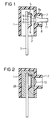
- Figure 1 in section in the inventive method used module housing with inserted carrier
- Figure 2 shows the completed electro-optical module in one with the sectional view corresponding to Figure 1
- in Figure 3 is a side view of the finished electro-optical Module with a first positioning device
- in Figure 4 is a side view of another completed electro-optical module with a second positioning device shown.
- a prefabricated module housing 1 used that is pot-shaped and at its in the Figure 1 lower side with a relatively large opening 2 for Introducing a carrier 3 is provided.
- a carrier 3 for example, a so-called lead Frame can act, an electro-optical converter 4 is exact positioned applied in a previous process step and electrically via electrical conductors 5 and 6 connected to the carrier 3.
- Figure 1 also shows that the module housing 1 also with a nozzle 7 is provided, which has a receptacle for receiving a coupling partner, not shown, of the one to be manufactured represents electro-optical module.
- a housing part 8 which on its carrier 3 facing side 9 has an outer contour that one in this area to be formed functional surface 10, z.
- the Housing part 8 is at its edge as a predetermined breaking point 8a formed and has a termination process 11, the the nozzle 7 protrudes outwards.
- Figures 3 and 4 show how the carrier 3 with the electro-optical Converter 4 precisely positioned in the module housing 1 can be accommodated in a position as shown in FIG. 1 reveals.
- a positioning device 12 is provided in the module housing 1, the positioning lugs 13 attached to the outside of the module housing 1 and has 14; with these positioning lugs 13 and 14 Positioning hooks 15 and 16 work together on the carrier 3 are provided.
- the positioning hooks 15 and 16 with wedge-shaped Recesses 17 and 18 against correspondingly wedge-shaped trained ends 19 and 20 of the adjustment lugs of the module housing 1 led and put together.
- another positioning device is used used.
- This contains recesses 21 and 22 on the inside of the module housing 1; in the Locking recesses 21 and 22 engage locking lugs 23 and 24 a, which are formed by the carrier 3.
- stop elements 25 and 26 ensure an accurate Positioning and holding the carrier 3 in the module housing 1, because they led against the front face 27 of the module housing 1 be, whereby a latching of the carrier 3 in the module housing 1 occurs.
- the finished electro-optical module is shown in FIG in the same sectional view as shown in Figure 1.
- the module housing 1 now with a translucent, mouldable material 28 filled, which after introduction to a Shaped body is cured.
- the housing part 8 removed from the nozzle 7, whereby the functional surface 10 is exposed.
Landscapes
- Physics & Mathematics (AREA)
- General Physics & Mathematics (AREA)
- Optics & Photonics (AREA)
- Optical Couplings Of Light Guides (AREA)
- Casting Or Compression Moulding Of Plastics Or The Like (AREA)
- Light Receiving Elements (AREA)
Abstract
Description
Claims (11)
- Verfahren zum Herstellen eines elektrooptisches Moduls mit einem Formkörper aus einem lichtdurchlässigen, formbaren Material, bei demein Träger mit einer Positioniereinrichtung und mit mindestens einem ausgerichtet aufgebrachten elektrooptischen Wandler mittels des Positioniereinrichtung exakt in einer Gießform positioniert wird undder Träger mit dem Wandler zumindest teilweise mit dem formbaren Material unter Bildung des Formkörpers umgeben wird,dadurch gekennzeichnet, daßwobei der Formkörper mindestens eine der Kopplung mit einem Kopplungspartner dienende Funktionsfläche erhält,als Gießform ein Modulgehäuse (1) mit einer Öffnung (2) zum Einführen des Trägers (3) und mit einem Ankopplungsbereich für den Kopplungspartner verwendet wird, wobeisich im Ankopplungsbereich ein Gehäuseteil (8) befindet, das an seiner inneren Seite (9) der Außenkontur der Funktionsfläche (10) entsprechend gestaltet ist, undder Formkörper durch Einfüllen des formbaren Materials (28) in das Modulgehäuse (1) gebildet wird.
- Verfahren nach Anspruch 1,
dadurch gekennzeichnet, daßdas ein an seinem Rand eine Sollbruchstelle (8a) aufweisendes Gehäuseteil (8) verwendet wird. - Verfahren nach Anspruch 1 oder 2,
dadurch gekennzeichnet, daßals Gießform ein Modulgehäuse (1) mit einem Ankopplungsbereich verwendet wird, der als ein eine Steckbucht zur Aufnahme des Kopplungspartners bildender Stutzen (7) gestaltet ist. - Verfahren nach einem der vorangehenden Ansprüche,
dadurch gekennzeichnet, daßdas an seiner äußeren Seite mit einem Abbruchfortsatz (11) versehene Gehäuseteil (8) nach der Bildung des Formkörpers (28) durch Krafteinwirkung auf den Abbruchfortsatz (11) aus dem Modulgehäuse (1) entfernt wird. - Verfahren nach einem der vorangehenden Ansprüche,
dadurch gekennzeichnet, daßals Positioniereinrichtung Ansätze (15, 16, 23, 24) an dem Träger (3) dienen, die beim Positionieren des Trägers (3) mit dem Wandler in dem Modulgehäuse (1) mit dem Modulgehäuse verbunden werden. - Gießform zum Herstellen eines optisches Moduls mit einem Formkörper aus einem lichtdurchlässigen, formbaren Material, bei demein Träger mit einer Positioniereinrichtung und mit mindestens einem ausgerichtet aufgebrachten elektrooptischen Wandler mittels der Positioniereinrichtung exakt in der Gießform positioniert wird undder Träger mit dem Wandler zumindest teilweise mit dem formbaren Material unter Bildung des Formkörpers umgeben wird,dadurch gekennzeichnet, daßwobei der Formkörper mindestens eine der Kopplung mit einem Kopplungspartner dienende Funktionsfläche erhält,die Gießform ein Modulgehäuse (1) mit einer Öffnung (2) zum Einführen des Trägers (3) und mit einem Ankopplungsbereich für den Kopplungspartner ist undsich im Ankopplungsbereich ein Gehäuseteil (8) befindet, das an seiner inneren Seite(9) der Außenkontur der Funktionsfläche (10) entsprechend gestaltet ist.
- Gießform nach Anspruch 6,
dadurch gekennzeichnet, daßdas Gehäuseteil (8) an seinem Rand eine Sollbruchstelle (8a) aufweist. - Gießform nach Anspruch 6 oder 7,
dadurch gekennzeichnet, daßder Ankopplungsbereich als ein eine Steckbucht zur Aufnahme des Kopplungspartners bildender Stutzen (7) ausgebildet ist. - Gießform nach einem der Ansprüche 6 bis 8,
dadurch gekennzeichnet, daßdas Gehäuseteil (8) an seiner äußeren Seite einen Abbruchfortsatz (11) trägt. - Elektrooptisches Modul mit einem Formkörper aus einem lichtdurchlässigen, formbaren Material, bei demein Träger mit einem elektrooptischen Wandler zumindest teilweise mit dem formbaren Material unter Bildung des Formkörpers umgeben ist,dadurch gekennzeichnet, daßwobei der Formkörper mindestens eine der Kopplung mit einem Kopplungspartner dienende Funktionsfläche erhält,das Modul ein Modulgehäuse (1) mit einer Öffnung (2) zum Einführen des Trägers (3) und mit einem Ankopplungsbereich für den Kopplungspartner aufweist,das Modulgehäuse (1) mit dem formbaren Material (28) gefüllt ist,sich im Ankopplungsbereich eine Funktionsfläche (10) befindet, die beim Füllen des Modulgehäuses (1) mit dem formbaren Material (28) durch ein an seiner inneren Seite (9) der Außenkontur der Funktionsfläche (10) entsprechend gestaltetes und danach entferntes Gehäuseteil (8) gebildet ist.
- Modul nach Anspruch 10,
dadurch gekennzeichnet, daßdas Modulgehäuse (1) einen Ankopplungsbereich aufweist, der als ein eine Steckbucht zur Aufnahme des Kopplungspartners bildender Stutzen (7) ausgebildet ist.
Applications Claiming Priority (2)
| Application Number | Priority Date | Filing Date | Title |
|---|---|---|---|
| DE19909242A DE19909242A1 (de) | 1999-02-22 | 1999-02-22 | Verfahren und Gießform zum Herstellen eines elektrooptischen Moduls und elektrooptisches Modul |
| DE19909242 | 1999-02-22 |
Publications (3)
| Publication Number | Publication Date |
|---|---|
| EP1031860A2 true EP1031860A2 (de) | 2000-08-30 |
| EP1031860A3 EP1031860A3 (de) | 2002-08-28 |
| EP1031860B1 EP1031860B1 (de) | 2004-10-27 |
Family
ID=7899526
Family Applications (1)
| Application Number | Title | Priority Date | Filing Date |
|---|---|---|---|
| EP20000102995 Expired - Lifetime EP1031860B1 (de) | 1999-02-22 | 2000-02-14 | Verfahren und Gie form zur Herstellung eines elektrooptischen Moduls und elektrooptisches Modul |
Country Status (4)
| Country | Link |
|---|---|
| US (1) | US6309566B1 (de) |
| EP (1) | EP1031860B1 (de) |
| JP (1) | JP2000243980A (de) |
| DE (2) | DE19909242A1 (de) |
Cited By (2)
| Publication number | Priority date | Publication date | Assignee | Title |
|---|---|---|---|---|
| WO2009028159A1 (en) * | 2007-08-24 | 2009-03-05 | Yazaki Corporation | Housing-integrated optical semiconductor component and manufacturing method thereof |
| EP2063302A1 (de) * | 2007-11-20 | 2009-05-27 | Nitto Denko Corporation | Verfahren zur Herstellung einer optischen Wellenleitervorrichtung und Wellenleiterverbindungsstruktur |
Families Citing this family (35)
| Publication number | Priority date | Publication date | Assignee | Title |
|---|---|---|---|---|
| DE19918860C2 (de) * | 1999-04-26 | 2002-03-07 | Tyco Electronics Logistics Ag | Elektro-optisches Wandlerbauteil und Verfahren zu seiner Herstellung |
| DE19939364B4 (de) * | 1999-08-19 | 2005-02-03 | Tyco Electronics Logistics Ag | Verfahren und Gießform zum Herstellen eines elektrooptischen Bauteils |
| DE19959781C2 (de) * | 1999-12-07 | 2003-02-20 | Infineon Technologies Ag | Opto-elektronische Baugruppe mit integriertem Abbildungs-System |
| DE10001875C2 (de) * | 2000-01-18 | 2002-01-24 | Infineon Technologies Ag | Optisches Sende-/Empfangsmodul mit internem Lichtwellenleiter |
| DE10058741B4 (de) * | 2000-11-27 | 2006-03-30 | Bayerische Motoren Werke Ag | Optoelektronisches Bauelement mit einem Umgehäuse und Verfahren zu seiner Herstellung |
| DE10151113B4 (de) | 2001-10-15 | 2004-03-25 | Infineon Technologies Ag | Opto-elektronisches Modul und Verfahren zu seiner Herstellung |
| EP1483613B1 (de) | 2002-03-08 | 2011-10-12 | Avago Technologies Fiber IP (Singapore) Pte. Ltd. | Aufnahme- und koppelteil für ein opto-elektronisches sende- element |
| WO2003076998A1 (de) | 2002-03-08 | 2003-09-18 | Infineon Technologies Ag | Optoelektronisches modul und steckeranordnung |
| DE10237403B4 (de) | 2002-08-12 | 2004-07-29 | Infineon Technologies Ag | Opto-elektronisches Sende- und/oder Empfangsmodul und optischer Stecker |
| EP1391763A1 (de) * | 2002-08-13 | 2004-02-25 | Tyco Electronics AMP GmbH | Optoelektronisches Modul |
| DE10250540B3 (de) * | 2002-10-29 | 2004-07-15 | Infineon Technologies Ag | Verfahren zur Herstellung eines optoelektronischen Bauteiles |
| EP1447696B1 (de) | 2003-02-04 | 2008-07-30 | Avago Technologies Fiber IP (Singapore) Pte. Ltd. | Modulares optoelektronisches Bauelement |
| DE10319900A1 (de) | 2003-04-29 | 2004-11-25 | Infineon Technologies Ag | Optoelektronische Sende- und/oder Empfangsanordnung |
| DE10321257B4 (de) * | 2003-05-06 | 2006-04-27 | Infineon Technologies Ag | Optische oder optoelektronische Anordnung mit mindestens einem auf einem Metallträger angeordneten optoelektronischen Bauelement |
| DE10322757B4 (de) | 2003-05-19 | 2012-08-30 | Avago Technologies Fiber Ip (Singapore) Pte. Ltd. | Optoelektronische Sende- und/oder Empfangsanordnungen |
| DE10329988B3 (de) | 2003-06-27 | 2005-01-13 | Infineon Technologies Ag | Opto-elektronische Sende- und/oder Empfangsanordnung |
| FR2860600A1 (fr) * | 2003-10-07 | 2005-04-08 | Framatome Connectors Int | Module optoelectronique et procede de fabrication associe |
| DE502004003608D1 (de) | 2004-03-04 | 2007-06-06 | Infineon Technologies Ag | Verfahren zur Ausrichtung eines Lichtwellenleiters in Bezug auf eine optische Einheit eines optischen Moduls, optisches Modul und Bausatz mit einem optischen Modul |
| EP1622204B9 (de) | 2004-07-28 | 2009-11-11 | Avago Technologies Fiber IP (Singapore) Pte. Ltd. | Verfahren zum Herstellen eines mit einem Kunststoffgehäuse versehenen optischen oder elektronischen Moduls |
| EP1622237A1 (de) * | 2004-07-28 | 2006-02-01 | Infineon Technologies Fiber Optics GmbH | Optisches oder elektronisches Modul und Verfahren zu dessen Herstellung |
| EP1630913B1 (de) * | 2004-08-31 | 2007-10-03 | Infineon Technologies AG | Verfahren zum Herstellen eines mit einem Kunststoffgehäuse versehenen optischen oder elektronischen Moduls das eine optische oder elektronische Komponente enthält, sowie optisches oder elektronisches Modul |
| KR100722617B1 (ko) * | 2004-10-08 | 2007-05-28 | 삼성전기주식회사 | 광변조기 모듈 패키지 구조 |
| EP1655628A1 (de) | 2004-10-27 | 2006-05-10 | Infineon Technologies Fiber Optics GmbH | Verfahren zur optischen Kopplung eines Lichtwellenleiters mit einer optischen Einheit eines optischen Moduls, optisches Modul, Koppelement für ein optisches Modul und Bausatz mit einer Mehrzahl von Koppelelementen |
| US7500792B2 (en) | 2004-11-26 | 2009-03-10 | Finisar Corporation | Optoelectronic transmitting and/or receiving arrangement |
| DE102007044554B3 (de) * | 2007-07-18 | 2009-07-16 | Siemens Ag | Sensorband mit optischer Sensorfaser, Sensor mit diesem Sensorband und Verfahren zum Kalibrieren einer optischen Sensorfaser |
| KR101542809B1 (ko) | 2008-08-25 | 2015-08-07 | 삼성전자주식회사 | 비접촉 통신이 가능한 광 단자, 광 연결장치, 및 이를 이용한 전자기기 제조방법 |
| US8265487B2 (en) * | 2009-07-29 | 2012-09-11 | Avago Technologies Fiber Ip (Singapore) Pte. Ltd. | Half-duplex, single-fiber (S-F) optical transceiver module and method |
| DE102009038523A1 (de) | 2009-08-25 | 2011-03-10 | Odelo Gmbh | Leuchtmittel sowie Leuchte |
| US8842951B2 (en) | 2012-03-02 | 2014-09-23 | Analog Devices, Inc. | Systems and methods for passive alignment of opto-electronic components |
| US9716193B2 (en) | 2012-05-02 | 2017-07-25 | Analog Devices, Inc. | Integrated optical sensor module |
| US10884551B2 (en) | 2013-05-16 | 2021-01-05 | Analog Devices, Inc. | Integrated gesture sensor module |
| US9590129B2 (en) | 2014-11-19 | 2017-03-07 | Analog Devices Global | Optical sensor module |
| DE102015116355A1 (de) | 2015-09-28 | 2017-03-30 | Endress+Hauser Conducta Gmbh+Co. Kg | Behälter mit Sensoranordnung |
| US10712197B2 (en) | 2018-01-11 | 2020-07-14 | Analog Devices Global Unlimited Company | Optical sensor package |
| US10598860B2 (en) * | 2018-03-14 | 2020-03-24 | Globalfoundries Inc. | Photonic die fan out package with edge fiber coupling interface and related methods |
Family Cites Families (9)
| Publication number | Priority date | Publication date | Assignee | Title |
|---|---|---|---|---|
| US3389267A (en) * | 1965-09-10 | 1968-06-18 | Clairex Corp | Photoelectric cell with heat sink |
| GB2162335B (en) * | 1984-07-25 | 1988-07-13 | Adc Telecommunications Inc | Fibre optic coupler |
| EP0450560B1 (de) * | 1990-04-03 | 1998-07-22 | Sumitomo Electric Industries, Ltd. | Optische Vorrichtung |
| GB2316225A (en) * | 1996-08-06 | 1998-02-18 | Northern Telecom Ltd | Semiconductor photodetector packaging |
| DE19641393A1 (de) * | 1996-08-28 | 1998-06-10 | Siemens Ag | Elektrooptisches Modul |
| DE19641395A1 (de) * | 1996-08-28 | 1998-05-28 | Siemens Ag | Verfahren zum Herstellen eines elektrooptischen Moduls |
| US5763900A (en) * | 1996-12-05 | 1998-06-09 | Taiwan Liton Electronic Co. Ltd. | Infrared transceiver package |
| DE19711138C2 (de) * | 1997-03-07 | 1998-12-17 | Siemens Ag | Herstellungsverfahren für ein elektrooptisches Modul |
| JP2000110176A (ja) * | 1998-10-02 | 2000-04-18 | Fujitsu Ltd | 光モジュール及びその製造方法 |
-
1999
- 1999-02-22 DE DE19909242A patent/DE19909242A1/de not_active Ceased
-
2000
- 2000-02-14 EP EP20000102995 patent/EP1031860B1/de not_active Expired - Lifetime
- 2000-02-14 DE DE50008375T patent/DE50008375D1/de not_active Expired - Lifetime
- 2000-02-22 JP JP2000044922A patent/JP2000243980A/ja active Pending
- 2000-02-22 US US09/523,154 patent/US6309566B1/en not_active Expired - Lifetime
Cited By (4)
| Publication number | Priority date | Publication date | Assignee | Title |
|---|---|---|---|---|
| WO2009028159A1 (en) * | 2007-08-24 | 2009-03-05 | Yazaki Corporation | Housing-integrated optical semiconductor component and manufacturing method thereof |
| US8602661B2 (en) | 2007-08-24 | 2013-12-10 | Yazaki Corporation | Housing-integrated optical semiconductor component and manufacturing method thereof |
| EP2063302A1 (de) * | 2007-11-20 | 2009-05-27 | Nitto Denko Corporation | Verfahren zur Herstellung einer optischen Wellenleitervorrichtung und Wellenleiterverbindungsstruktur |
| US7906355B2 (en) | 2007-11-20 | 2011-03-15 | Nitto Denko Corporation | Optical waveguide device production method, optical waveguide device produced by the method, and optical waveguide connection structure to be used for the device |
Also Published As
| Publication number | Publication date |
|---|---|
| EP1031860A3 (de) | 2002-08-28 |
| DE19909242A1 (de) | 2000-08-31 |
| DE50008375D1 (de) | 2004-12-02 |
| JP2000243980A (ja) | 2000-09-08 |
| US6309566B1 (en) | 2001-10-30 |
| EP1031860B1 (de) | 2004-10-27 |
Similar Documents
| Publication | Publication Date | Title |
|---|---|---|
| EP1031860B1 (de) | Verfahren und Gie form zur Herstellung eines elektrooptischen Moduls und elektrooptisches Modul | |
| DE69519938T2 (de) | Kapsel für ein optoelektrisches bauelement mit einer optischen schnittstelle | |
| DE3203259A1 (de) | Form fuer dentalmodelle | |
| DE10234778A1 (de) | Chip-Leiterplatten-Anordnung für optische Mäuse und zugehöriger Linsendeckel | |
| DE3004437A1 (de) | Verfahren zum herstellen eines magnetdomaenen-bauelements | |
| WO2010060410A1 (de) | Komponententräger für im wesentlichen elektrische bauelemente | |
| EP0429877B1 (de) | Vorrichtung zum Positionieren von Lichtleitfasern in Verbindungselementen | |
| DE69834870T2 (de) | Ausrichtsystem für einen faseroptischen Steckerstift | |
| DE3438435C2 (de) | Gehäuse aus Metall und Kunststoff für eine Halbleiter-Vorrichtung, das zur Befestigung an einem nicht genau ebenen Wärmeableiter geeignet ist, sowie Verfahren zu dessen Herstellung | |
| EP0804329B1 (de) | Verfahren zum dünnwandigen umgiessen einer zu der umgossenen wand genau ausgerichteten elektronikschaltung und elektronikschaltung hierzu | |
| WO2003077002A1 (de) | Aufnahme- und koppelteil für ein opto-elektronisches sende- und/oder empfangselement | |
| DE69520073T2 (de) | Verfahren zur Einkapselung eines optischen Bauelements unter Verwendung eines dafür angepassten Leiterrrahmens | |
| DE19743992C1 (de) | Verfahren zum Herstellen eines optoelektronischen Steckeraufnahmeelementes und optoelektronischer Stecker | |
| DE3150435A1 (de) | Verfahren zum herstellen eines elektrischen bauteils | |
| EP0817116A2 (de) | Chipkarte sowie Verfahren und Herstellung einer Chipkarte | |
| DE3440110C1 (de) | Verfahren zur Herstellung mechanisch trennbarer Vielfach-Verbindungen fuer den elektrischen Anschluss mikroelektronischer Bauelemente | |
| EP0731365B1 (de) | Verfahren zur Herstellung eines elektrooptischen Bauelements | |
| DE2931357C2 (de) | Verfahren zum Herstellen eines vollständigen elektronischen Uhren-Bausteins | |
| DE10328005B3 (de) | Verfahren zur Herstellung eines Komponententrägers für elektrische Bauelemente | |
| DE4438053C2 (de) | Verfahren zum Herstellen einer elektrisch leitfähigen Struktur | |
| DE69032335T2 (de) | Verfahren zur Einkapselung einer integrierten Schaltung auf einem Träger, Anordnung zur Benutzung dieses Verfahrens und eine nach diesem Verfahren hergestellte elektronische Anordnung | |
| DE3343028C2 (de) | Vorrichtung für die Herstellung eines Tintendruckkopfes | |
| DD151523A5 (de) | Tonabnehmer mit beweglichem magneten und verfahren zu seiner herstellung | |
| DE69513520T2 (de) | Steckervorrichtung | |
| DE102023203712B3 (de) | Vorrichtung zum Herstellen eines Innenverkleidungsteils |
Legal Events
| Date | Code | Title | Description |
|---|---|---|---|
| PUAI | Public reference made under article 153(3) epc to a published international application that has entered the european phase |
Free format text: ORIGINAL CODE: 0009012 |
|
| AK | Designated contracting states |
Kind code of ref document: A2 Designated state(s): AT BE CH CY DE DK ES FI FR GB GR IE IT LI LU MC NL PT SE |
|
| AX | Request for extension of the european patent |
Free format text: AL;LT;LV;MK;RO;SI |
|
| PUAL | Search report despatched |
Free format text: ORIGINAL CODE: 0009013 |
|
| AK | Designated contracting states |
Kind code of ref document: A3 Designated state(s): AT BE CH CY DE DK ES FI FR GB GR IE IT LI LU MC NL PT SE |
|
| AX | Request for extension of the european patent |
Free format text: AL;LT;LV;MK;RO;SI |
|
| 17P | Request for examination filed |
Effective date: 20021118 |
|
| AKX | Designation fees paid |
Designated state(s): DE FR GB |
|
| 17Q | First examination report despatched |
Effective date: 20030506 |
|
| GRAP | Despatch of communication of intention to grant a patent |
Free format text: ORIGINAL CODE: EPIDOSNIGR1 |
|
| GRAS | Grant fee paid |
Free format text: ORIGINAL CODE: EPIDOSNIGR3 |
|
| GRAA | (expected) grant |
Free format text: ORIGINAL CODE: 0009210 |
|
| AK | Designated contracting states |
Kind code of ref document: B1 Designated state(s): DE FR GB |
|
| REG | Reference to a national code |
Ref country code: GB Ref legal event code: FG4D Free format text: NOT ENGLISH |
|
| RIN1 | Information on inventor provided before grant (corrected) |
Inventor name: HURT, HANS Inventor name: MUELLER, GUSTAV DR. |
|
| REG | Reference to a national code |
Ref country code: IE Ref legal event code: FG4D Free format text: GERMAN |
|
| REF | Corresponds to: |
Ref document number: 50008375 Country of ref document: DE Date of ref document: 20041202 Kind code of ref document: P |
|
| GBT | Gb: translation of ep patent filed (gb section 77(6)(a)/1977) |
Effective date: 20050131 |
|
| REG | Reference to a national code |
Ref country code: IE Ref legal event code: FD4D |
|
| PLBE | No opposition filed within time limit |
Free format text: ORIGINAL CODE: 0009261 |
|
| STAA | Information on the status of an ep patent application or granted ep patent |
Free format text: STATUS: NO OPPOSITION FILED WITHIN TIME LIMIT |
|
| ET | Fr: translation filed | ||
| 26N | No opposition filed |
Effective date: 20050728 |
|
| REG | Reference to a national code |
Ref country code: GB Ref legal event code: 732E |
|
| PGFP | Annual fee paid to national office [announced via postgrant information from national office to epo] |
Ref country code: FR Payment date: 20070212 Year of fee payment: 8 |
|
| REG | Reference to a national code |
Ref country code: FR Ref legal event code: ST Effective date: 20081031 |
|
| PG25 | Lapsed in a contracting state [announced via postgrant information from national office to epo] |
Ref country code: FR Free format text: LAPSE BECAUSE OF NON-PAYMENT OF DUE FEES Effective date: 20080229 |
|
| REG | Reference to a national code |
Ref country code: DE Ref legal event code: R082 Ref document number: 50008375 Country of ref document: DE Representative=s name: DILG HAEUSLER SCHINDELMANN PATENTANWALTSGESELL, DE |
|
| REG | Reference to a national code |
Ref country code: DE Ref legal event code: R081 Ref document number: 50008375 Country of ref document: DE Owner name: AVAGO TECHNOLOGIES GENERAL IP (SINGAPORE) PTE., SG Free format text: FORMER OWNER: AVAGO TECHNOLOGIES FIBER IP (SINGAPORE) PTE. LTD., SINGAPORE, SG Effective date: 20130812 Ref country code: DE Ref legal event code: R082 Ref document number: 50008375 Country of ref document: DE Representative=s name: DILG HAEUSLER SCHINDELMANN PATENTANWALTSGESELL, DE Effective date: 20130812 |
|
| PGFP | Annual fee paid to national office [announced via postgrant information from national office to epo] |
Ref country code: GB Payment date: 20160127 Year of fee payment: 17 |
|
| GBPC | Gb: european patent ceased through non-payment of renewal fee |
Effective date: 20170214 |
|
| PG25 | Lapsed in a contracting state [announced via postgrant information from national office to epo] |
Ref country code: GB Free format text: LAPSE BECAUSE OF NON-PAYMENT OF DUE FEES Effective date: 20170214 |
|
| REG | Reference to a national code |
Ref country code: DE Ref legal event code: R082 Ref document number: 50008375 Country of ref document: DE Representative=s name: DILG HAEUSLER SCHINDELMANN PATENTANWALTSGESELL, DE Ref country code: DE Ref legal event code: R081 Ref document number: 50008375 Country of ref document: DE Owner name: AVAGO TECHNOLOGIES INTERNATIONAL SALES PTE. LT, SG Free format text: FORMER OWNER: AVAGO TECHNOLOGIES GENERAL IP (SINGAPORE) PTE. LTD., SINGAPORE, SG |
|
| PGFP | Annual fee paid to national office [announced via postgrant information from national office to epo] |
Ref country code: DE Payment date: 20190122 Year of fee payment: 20 |
|
| REG | Reference to a national code |
Ref country code: DE Ref legal event code: R071 Ref document number: 50008375 Country of ref document: DE |