EP1032028B1 - Dispositif MOS amélioré à tranchée - Google Patents
Dispositif MOS amélioré à tranchée Download PDFInfo
- Publication number
- EP1032028B1 EP1032028B1 EP00102399A EP00102399A EP1032028B1 EP 1032028 B1 EP1032028 B1 EP 1032028B1 EP 00102399 A EP00102399 A EP 00102399A EP 00102399 A EP00102399 A EP 00102399A EP 1032028 B1 EP1032028 B1 EP 1032028B1
- Authority
- EP
- European Patent Office
- Prior art keywords
- layer
- region
- trench
- portions
- conductivity
- Prior art date
- Legal status (The legal status is an assumption and is not a legal conclusion. Google has not performed a legal analysis and makes no representation as to the accuracy of the status listed.)
- Expired - Lifetime
Links
Images




Classifications
-
- H—ELECTRICITY
- H10—SEMICONDUCTOR DEVICES; ELECTRIC SOLID-STATE DEVICES NOT OTHERWISE PROVIDED FOR
- H10D—INORGANIC ELECTRIC SEMICONDUCTOR DEVICES
- H10D30/00—Field-effect transistors [FET]
- H10D30/60—Insulated-gate field-effect transistors [IGFET]
- H10D30/64—Double-diffused metal-oxide semiconductor [DMOS] FETs
- H10D30/66—Vertical DMOS [VDMOS] FETs
- H10D30/668—Vertical DMOS [VDMOS] FETs having trench gate electrodes, e.g. UMOS transistors
-
- H—ELECTRICITY
- H10—SEMICONDUCTOR DEVICES; ELECTRIC SOLID-STATE DEVICES NOT OTHERWISE PROVIDED FOR
- H10D—INORGANIC ELECTRIC SEMICONDUCTOR DEVICES
- H10D30/00—Field-effect transistors [FET]
- H10D30/60—Insulated-gate field-effect transistors [IGFET]
-
- H—ELECTRICITY
- H10—SEMICONDUCTOR DEVICES; ELECTRIC SOLID-STATE DEVICES NOT OTHERWISE PROVIDED FOR
- H10D—INORGANIC ELECTRIC SEMICONDUCTOR DEVICES
- H10D64/00—Electrodes of devices having potential barriers
- H10D64/20—Electrodes characterised by their shapes, relative sizes or dispositions
- H10D64/27—Electrodes not carrying the current to be rectified, amplified, oscillated or switched, e.g. gates
- H10D64/311—Gate electrodes for field-effect devices
- H10D64/411—Gate electrodes for field-effect devices for FETs
- H10D64/511—Gate electrodes for field-effect devices for FETs for IGFETs
- H10D64/512—Disposition of the gate electrodes, e.g. buried gates
- H10D64/513—Disposition of the gate electrodes, e.g. buried gates within recesses in the substrate, e.g. trench gates, groove gates or buried gates
-
- H—ELECTRICITY
- H10—SEMICONDUCTOR DEVICES; ELECTRIC SOLID-STATE DEVICES NOT OTHERWISE PROVIDED FOR
- H10D—INORGANIC ELECTRIC SEMICONDUCTOR DEVICES
- H10D30/00—Field-effect transistors [FET]
- H10D30/01—Manufacture or treatment
- H10D30/021—Manufacture or treatment of FETs having insulated gates [IGFET]
- H10D30/028—Manufacture or treatment of FETs having insulated gates [IGFET] of double-diffused metal oxide semiconductor [DMOS] FETs
- H10D30/0291—Manufacture or treatment of FETs having insulated gates [IGFET] of double-diffused metal oxide semiconductor [DMOS] FETs of vertical DMOS [VDMOS] FETs
- H10D30/0297—Manufacture or treatment of FETs having insulated gates [IGFET] of double-diffused metal oxide semiconductor [DMOS] FETs of vertical DMOS [VDMOS] FETs using recessing of the gate electrodes, e.g. to form trench gate electrodes
-
- H—ELECTRICITY
- H10—SEMICONDUCTOR DEVICES; ELECTRIC SOLID-STATE DEVICES NOT OTHERWISE PROVIDED FOR
- H10D—INORGANIC ELECTRIC SEMICONDUCTOR DEVICES
- H10D64/00—Electrodes of devices having potential barriers
- H10D64/01—Manufacture or treatment
- H10D64/025—Manufacture or treatment forming recessed gates, e.g. by using local oxidation
- H10D64/027—Manufacture or treatment forming recessed gates, e.g. by using local oxidation by etching at gate locations
-
- H—ELECTRICITY
- H10—SEMICONDUCTOR DEVICES; ELECTRIC SOLID-STATE DEVICES NOT OTHERWISE PROVIDED FOR
- H10P—GENERIC PROCESSES OR APPARATUS FOR THE MANUFACTURE OR TREATMENT OF DEVICES COVERED BY CLASS H10
- H10P30/00—Ion implantation into wafers, substrates or parts of devices
- H10P30/20—Ion implantation into wafers, substrates or parts of devices into semiconductor materials, e.g. for doping
- H10P30/22—Ion implantation into wafers, substrates or parts of devices into semiconductor materials, e.g. for doping using masks
Definitions
- This invention relates to the manufacture of semiconductor devices including MOS transistor components disposed along the side walls of trenches formed on an "upper" surface of a semiconductor chip.
- a trench is etched entirely through the second layer and extends into the first layer, the trench having a contiguous wall comprised of exposed surfaces of said first and second layers.
- a dielectric material third layer is formed on that wall, and at least portion of said dielectric material layer is covered with an electrically conductive layer.
- First dopants are introduced into the second layer for converting a first region of said second layer to a conductivity greater than the conductivity of the second layer, said first region being contiguous with a portion of the trench wall contiguous with said dielectric material layer covered, in turn, with said conductive material, and said first region being spaced within said second layer, from the interface between the first and second layers.
- a typical MOS transistor component (forming part of semiconductor devices such as insulated bipolar transistors, MOS controlled thyristors, and MOS transistors) comprises source and drain regions of the same conductivity type separated by a channel region of opposite type conductivity. Conduction of charge carriers from the source region to the drain region through the channel region is controlled by a voltage applied to a gate electrode overlying the channel region and separated therefrom by a thin layer of a dielectric material. With chips of silicon, the dielectric material is typically silicon dioxide.
- a starting workpiece comprises a silicon chip comprising an "underlying" substrate of relatively heavily doped silicon, e.g., of N type, an intermediate silicon layer interfacing with the substrate and, in this example, lightly doped N type, and an overlying silicon layer "moderately” doped, of P type.
- the intermediate layer and substrate comprise a drain region common to a plurality of MOS components (connected in parallel within a single or “discrete” power device), and the overlying layer comprises the channel region of each of the MOS components.
- Completion of the workpiece requires the addition of a source region, a gate oxide, and source and gate electrodes for each MOS component as well as a drain electrode for the common drain region.
- This is accomplished by first forming spaced apart regions of N type conductivity across the upper surface of the chip, e.g., by ion implantation.
- the N type regions extend only part way through the overlying P type layer and are to comprise the source regions of the MOS components.
- the spaced apart source regions are provided in a uniformly doped layer, i.e., without defined features, little precision is required in the process.
- trenches are then etched entirely through the overlying P layer through each of the source regions.
- the previously formed source regions are clearly visible and provide a means for precise alignment of the photomask used in the trench etching process.
- the trench walls are coated, e.g., in a thermal oxidation process, with a layer of silicon dioxide.
- the trenches are then filled with an electrically conductive material, e.g., doped polycrystalline silicon, which serves as the gate electrode of the MOS components formed vertically along the trench walls.
- the silicon dioxide layers covering the trench walls serve as the gate electrode dielectric layer of the various MOS components as well as an insulator at the bottoms of the trenches for electrically isolating the gate electrodes from the underlying drain regions.
- electrically conductive layers are provided on the chip surfaces serving as source and drain region electrodes and extensions of the gate electrodes.
- all the elements added to the initial chip workpiece are as small as possible, e.g., the trenches have the smallest widths achievable using known etching processes.
- the gate oxide layers are uniformly thin. Two basic problems are found to exist with the known manufacturing processes. One is that the trench walls are not uniformly straight and smooth, and the second is that the gate oxide layers are not uniformly thick. The effect of such structural variations is variations in electrical characteristics of the various MOS components. Ideally, all the MOS components should have identical shapes and dimensions and identical electrical characteristics. The present invention is directed toward reducing the structural variations among the MOS components and improving the uniformity of the electrical characteristics thereof.
- the present invention includes a method of fabricating a MOS device within a body of silicon material, the silicon material having a first layer of a first conductivity type having a first surface and a second layer forming an interface with said first surface, said second layer having a conductivity greater than that of said first layer and of a second conductivity type, said method comprising the steps of: etching a trench entirely through said second layer from a first surface thereof opposite to said interface, said trench extending through said interface into said first layer, said trench having respective continuous sidewalls comprised of exposed surfaces of said first and second layers; covering at least a portion of said sidewalls with a silicon dioxide material third layer, said portion including said interface; covering at least a portion of said silicon dioxide material third layer with an electrically conductive material, said step of covering comprising filling the trench with doped polysilicon material; thermally growing a silicon dioxide fourth layer on exposed surfaces of said body, said fourth layer including first portions overlying portions of said first surface of said second layer surrounding said trench and spaced therefrom by a gap
- the invention also includes a method of fabricating a MOS device within a body of silicon material, the silicon material having a first layer of a first conductivity type having a first surface and a second layer forming an interface with said first surface, said second layer having a conductivity greater than that of said first layer and of a second conductivity type, said method comprising the steps of: forming a silicon dioxide third layer on a first surface of the second layer opposite said interface and depositing an ion impenetrable mask; forming an opening in the mask and in the third layer exposing a portion of the second layer opposite said interface; etching a trench entirely through said exposed portion of the second layer, said trench extending through said interface into said first layer, said trench having respective continuous sidewalls comprised of exposed surfaces of said first and second layers; covering at least a portion of said sidewalls with a silicon dioxide material fourth layer, said portion including said interface; covering at least a portion of said silicon dioxide material fourth layer with an electrically conductive material, said step of covering comprising filling the trench with
- a known prior art process for fabricating MOS components of the "trench" type is first described.
- the known process is illustrated in Figs. 1-6 .
- the semiconductor device being fabricated is a known power MOS transistor.
- Fig. 1 shows a starting workpiece 8 comprising a semiconductor wafer including an underlying substrate 10, in this illustrative example, heavily doped silicon of N type conductivity.
- the substrate 10 has a thickness of around 0.025 inch and is cut from a grown single crystal of silicon.
- an intermediate layer 12 Overlying the substrate 10 is an intermediate layer 12, having a thickness of up to around 100 microns, overlaid by an upper layer 14 having a thickness of around 2 microns.
- the thickness dimensions are given to provide an indication of typical relative dimensions; the actual thickness can vary depending upon the actual devices being made and the processing techniques used.
- the intermediate layer 12 is epitaxially grown on a surface 15 of the substrate 10, and the upper layer 14 is formed by implantation and diffusion of ions into an upper portion of the intermediate layer 12.
- the substrate 10 is heavily doped (N + ) by arsenic or antimony ions at a concentration in a range of around 10 19 to 10 20 /cm 3 .
- the intermediate layer 12 is lightly doped (N - ) by arsenic ions at a concentration in a range of around 10 14 to 10 16 /cm 3 .
- the top layer 14 is moderately P doped, by boron ions, at a concentration in a range of around 10 15 to 10 17 /cm 3 .
- the illustrative doping concentrations indicate typical relative conductivities which can vary dependant upon the devices being made.
- a photolithographically patterned oxide layer 25 is used as an etch mask for etching a trench 26, by reactive ion etching (RIE), precisely positioned relative to the source region 24.
- RIE reactive ion etching
- the surface 18 of the P type layer 14 lies in the 100 crystal plane, and the vertical walls 28 of the trench are "intended to" lie in the 110 plane which, in the silicon crystal, is precisely perpendicular to the surface plane.
- the etched trench 26 extends entirely through the N.sup.+ source region 24, entirely through the P layer 14, and partly into the N layer 12.
- the rate of etching of silicon is a function both of the dopants present (typically phosphorous N dopant and boron P dopant) and the concentration of the dopants in the silicon.
- the rate of etching varies as the differently doped regions are encountered, variations in the slope of the trench walls occurs. This is illustrated, somewhat exaggerated, in FIG. 3 .
- the degree of slope variation is somewhat random and the actual trench shapes vary from trench to trench. Such variable trench profiles give rise to undesirable random variations in transistor electrical characteristics.
- the doping concentration in the region 24 is around four orders of magnitude greater than the doping concentration in the layer 14 (10.sup.19 versus 10.sup.15 at the low ends of the respective doping ranges and 10.sup.21 versus 10.sup.17 at the high ends thereof)
- Such (around) four orders of magnitude difference in doping concentration is generally sufficient to cause undesirably large etching rate variations.
- the walls of the trench are then oxidized, typically in a thermal oxidation process, to provide ( FIG. 4 ) a thin (e.g., 30-100 nm (300-1,000 A)) silicon dioxide layer 30.
- a problem, however, similar to that of etching the trench 26, is that the rate of oxidation of the silicon walls of the trench is a function of the dopants present and the concentration of the dopants.
- the rate of oxidation varies, with the result being, as shown exaggerated in FIG. 4 , that the thickness of the oxide layer 30 varies over a significant length of the layer 14 beginning at the junction 32.
- the thickness of the oxide layer 30 is critical with respect to transistor characteristics, and even quite small thickness variations from trench to trench result in significant variations in electrical characteristics of the various transistors. (Some variation in the rate of growth of the oxide layer 30 also occurs at the junction 16 between the P top layer 14 and the N - intermediate layer 12. However, the doping concentrations in these two layers 14 and 12 are relatively close, hence the variation in the rate of oxidation at the junction 16 therebetween is relatively small.)
- the trench is then filled ( Fig. 5 ) with a conductive material 34, typically doped polycrystalline silicon.
- a conductive material 34 typically doped polycrystalline silicon.
- the trench filling process comprises (as known) depositing polycrystalline silicon over the entire surface of the workpiece and then removing the unwanted polysilicon from everywhere over the portion of the workpiece shown except from within the trench using a known "planarization" process.
- the polysilicon material remaining in the trench 26 serves as a gate electrode in the completed device.
- the entire upper surface of the workpiece (all of which, including the polysilicon gate electrode 34, is covered with an oxide layer 35) is covered with a photoresist layer 36 which is patterned to expose an oxide covered surface portion 18a of the P layer 14 surrounding the source region 24.
- the surface portion 18a is spaced slightly away from the source region 24 by an edge 36a of the patterned masking layer 36.
- P type ions are then implanted through the exposed oxide layer and into the underlying surface portions 18a of the P type layer 14 for providing a P + type region 38 at the surface 18a of the layer 14 which, after drive-in, as shown in Fig. 6 , extends laterally beneath the edge 36a of the photoresist layer 36 and into electrical contact with the N source region 24.
- the trench structure shown in Fig. 6 is but one of a plurality of identical side-by-side trench structures disposed at the surface of the chip. The side edges of the chip portion illustrated are shown broken. If Fig. 6 were extended, e.g., to the right, the P + region 38 shown would extend into contact with a source region 24 of a trench structure identical to the structure shown in Fig. 6 .
- various electrically conductive layers are deposited on the workpiece for providing, electrode connections to (and shorting together) the doped regions 24 and 38, the bottom surface 40 ( Fig. 1 ) of the substrate 10, and the gate electrode 34.
- all the transistors on the chip are connected in parallel.
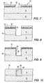
- Fig. 7 shows a workpiece 50 at a processing stage similar to that of the workpiece 8 shown in Fig. 1 .
- the Fig. 7 workpiece 50 comprises an N - type layer 12 (overlying an N+ silicon substrate, not shown), a P type layer 14, and patterned dielectric (20) and photoresist (22) layers having an opening 53 therethrough.
- the layer 20 is a thermally grown or a deposited (e.g., by CVD) oxide.
- the etched opening 23 through the two layers 22 and 20 is for the purpose of admitting dopant ions for the source region 24 ( Fig. 2 ).
- the opening 53 is not for the formation of the source region but, rather, as shown in Fig. 8 , the etching of a trench 56.
- the process of etching the trench 56 shown in Fig. 8 can be exactly the same as the etching of the trench 26 in Fig. 3 except that, and significantly, at the time of the etching process, a source region is not present and the etching occurs only through the P layer 14 and into the N - layer 12.
- the etching proceeds at a uniform rate through the uniformly doped P layer 14 and the side walls of the trench 56 are quite straight and smooth.
- the trench being etched reaches the junction 16 between the P layer 14 and the N - layer 12, some variation in the etch rate occurs, but in a manner somewhat unexpected from an examination of Fig. 3 . That is, rather than the rather large wall slope variations from the vertical present adjacent to the p-n junction 16 in Fig. 3 , only quite small slope variations are present in Fig. 8 .
- the walls of the trench are then coated ( FIG. 9 ) with a dielectric material, preferably a layer 60 of silicon dioxide provided in a known thermal oxidizing process.
- a dielectric material preferably a layer 60 of silicon dioxide provided in a known thermal oxidizing process.
- the workpiece shown in FIG. 9 is similar to the workpiece shown in FIG. 4 but with two exceptions. One is that the source region 24 shown in FIG. 4 is not present in the workpiece shown in FIG. 9 and, in direct consequence of the absence of such source region, the thickness of the grown oxide layer 60 is quite uniform along the thickness of the P layer 14.
- the oxide is also relatively uniformly thick because, as previously explained, the dopant concentrations in the P layer 14 and the N.sup.- layer 12 are relatively similar, and the rates of growth of the oxide layers on the two layers are also relatively similar.
- a layer of a conductive material preferably doped polycrystalline silicon, is deposited on the workpiece and of sufficient thickness to completely fill in the trench 56.
- a known process e.g., the aforementioned "planarizing" process, all the polysilicon material on the workpiece portion illustrated, except the polysilicon 64 within the trench 56, is removed. Any oxide and photoresist layers previously on the workpiece are also removed leaving a clean workpiece upper surface as shown in FIG. 10 .
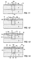
- FIG. 11 the entire upper surface of the workpiece is thermally oxidized for providing an oxide layer 68 (e.g., of thickness 30-40 nm (300-400 A)) on the workpiece surface.
- oxide layer 68 e.g., of thickness 30-40 nm (300-400 A
- the oxide layer is formed by the combination of oxygen with the silicon material on which the oxide is formed, and the thickness of the oxide is a function of the rate of oxidation of the silicon.
- Polycrystalline silicon oxidizes more rapidly (e.g., by a factor of around 3) than the monocrystalline silicon of the layer 14 and more rapidly than the edge of the silicon dioxide layer 60 exposed at the upper surface of the workpiece.
- the oxide layer 68 includes a thickened "cap" portion 68a. As shown in FIG.
- the thickness of the oxide cap 68a changes somewhat gradually with the result that the oxide cap 68a has a thickness, e.g., 90-120 nm (900-1200 A) where it overlies the filled in trench 56, a thickness, e.g., 40-90 nm (400-900 A) where it overlies the oxide layer 60, and a thickness decreasing to that of the oxide layer 68 where the cap 68a overlies a small portion 18b of the surface 18 of the P layer 14 adjoining the oxide layer 60.
- a thickness e.g., 90-120 nm (900-1200 A) where it overlies the filled in trench 56
- a thickness e.g., 40-90 nm (400-900 A) where it overlies the oxide layer 60
- a thickness decreasing to that of the oxide layer 68 where the cap 68a overlies a small portion 18b of the surface 18 of the P layer 14 adjoining the oxide layer 60 In subsequent steps, the result of which is shown in FIG.
- a photoresist layer 70 is provided on the workpiece and photolithographically patterned to provide an opening 72 therethrough exposing the trench oxide cap 68a and a portion 68b of the surface oxide 68 on the P layer 14 surrounding the oxide cap 68a.
- N type dopant ions are then implanted through the opening 72 to form an N doped region 74 (shown in dashed lines in FIG. 12 ) directly beneath the opening 72.
- the oxide cap 68a is thicker than the remainder of the oxide layer 68.
- the N type dopant ions e.g., phosphorous
- the N type dopant ions are implanted at an energy, e.g., 40-120 KeV, sufficient to penetrate the relatively thin oxide portion 68b and to enter into the P layer 14 but of insufficient energy to penetrate through the oxide cap 68a. Because the edges of the oxide cap 68a extend over and slightly beyond the gate electrode oxide layer 60, no dopants are injected into the oxide layer 60, and the implanted N doped region 74 is spaced slightly away from the oxide layer 60.
- the dopant region 74 is caused to expand into contact with the gate oxide layer 60 to form a source region 24, as shown in FIG. 13 .
- the workpiece shown in FIG. 13 (including a subsequently formed and patterned photoresist layer 76) is similar to the workpiece shown in FIG. 5 (but having straighter and smoother trench side walls and more uniformly thick gate oxide layers 60), and the subsequent steps used to complete the FIG. 5 workpiece can be used to complete the FIG. 13 workpiece.
- an oxide cap 68a ( FIG. 12 ) is used during ion implantation through a patterned photoresist layer 70 for masking the gate electrode 64 and the gate oxide layer 60 against the implanted ions.
- a workpiece 80 ( FIG. 14 ) is first processed to a configuration as shown in FIG. 10 ; i.e., a trench 56 has been filled with polysilicon 64 and both the excess silicon deposited during the trench filling step and the previously present ( FIG. 9 ) oxide layer 25 have been removed leaving the surface of the P layer exposed.
- an oxide layer 78 ( FIG.
- oxide layer 78 and oxide cap 78a having the appearance and disposition on the workpiece as the layer 68 and the cap 68a shown in FIG. 11 .
- oxide layers 78 and 78a are preferably (but not necessarily) thinner than the oxide layers 68 and 68a shown in FIG. 11 (and in FIG. 12 ).
- the oxide layer 78 can have a thickness of around 10-20 nm (100-200 A) (versus the aforementioned thickness of 30-40 nm (300-400 A) for the layer 68) and the oxide cap 78a has a thickness (at the thickest portion overlying the polysilicon 64) of, for example, 30-60nm (300-600 A) (versus 90-120 nm (900-1200 A) for the cap 68a).
- An advantage of the provision of thinner oxide layers 78 and 78a is that the oxidation process used to form the oxide layers 78 and 78a can be at lower temperatures and/or shorter duration than the process used to form the oxide layers 68 and 68a. The oxidation process is thus faster and less expensive.
- any thermal process used tends to disrupt and change the characteristics of previously formed doped regions. Accordingly, for least disruption of prior formed doped regions of the devices, low temperature processes are generally preferred over higher temperature processes.
- a photoresist layer is deposited on the workpiece surface and patterned to provide the masking layer 82.
- Fig. 14 is similar to Fig. 12 except that a portion 82a of the photoresist layer 82 overlies the relatively thin oxide cap 78a and adds to the thickness thereof.
- the combined oxide cap 78a and covering photoresist layer 82a quite effectively protect the gate electrode 64 and gate oxide layer 60 against contamination by ions implanted through an opening 83 through the layer 82 to form an N type region 74 (as in Fig. 12 ).
- a still further advantage of the use of a thinner oxide layer 78 is that lower ion implantation energies can be used for penetrating the relatively thin layer 78. Lower implantation energies result in greater control over the location and concentrations of the implanted ions and reduced ion damage.
- FIG. 15 A third embodiment of the invention is shown in Fig. 15 .
- a workpiece 90 has been processed to a condition such as shown in Fig. 12 , including a polysilicon gate electrode 64 filling a trench 56 including a gate oxide layer 60, an overlying oxide layer 68 including an oxide cap 68a.
- a difference between the workpiece shown in Fig. 12 and the workpiece shown in Fig. 15 is that, in Fig. 12 , a masking layer 70 is used during formation of the doped region 74.
- the opening 72 through the masking layer 70 defines what will become the "outer" edge 24a ( Fig. 13 ) of the source region 24, i.e., the edge of the source region later contacted by the subsequently implanted P + region 38.
- no masking layer similar to the Fig. 12 layer 70 is present.
- An N dopant implant is still made, however, with the thus implanted region 90 not having an "outer" edge such as the aforementioned outer edge 24a shown in Fig. 13 but extending to an adjacent trench structure as partially shown in Fig. 15 .
- an ion implantation mask such as the mask 70 shown in Fig. 12 , is not used and one photolithographic sequence is entirely eliminated.
- the workpiece is then heated for diffusing the implanted ions in the region 96 both downwardly and laterally.
- the result ( Fig. 16 ) is that the initially implanted region expands into a region 96a contacting the gate oxide layer 60. Although of large lateral extent, the region 96a is to form the transistor N type source region.
- a patterned etchant mask 98 is providedcovering the oxide cap 68a and an annular portion 100 of the oxide layer 68 surrounding the cap 68a. Relatively little precision is required in the patterning of the mask 98 because the more critical parameters of the source region 96a, i.e., its depth and its contacting relationship with the gate oxide layer 60, have already been defined and only less critical elements of the device remain to be formed.
- a central mesa structure is thus provided including a source region 96a surrounding the gate electrode 64 and contacting the gate oxide layer 60.
- P type ions are implanted ( FIG. 17 ) to form a P.sup.+ region 106 which, after a subsequent heating (diffusion) step, is driven laterally to first underlie the source region 96a and then upwardly to partially merge (as shown by region 106a in FIG. 18 ) with an outer edge portion 108 of the source region 96a spaced from the gate oxide layer 60.
- the workpiece 90 although containing a mesa structure, is basically identical to the workpiece 50 shown in FIG. 13 and can be similarly thereafter processed.
- FIG. 19 A fourth embodiment of the invention is shown in FIG. 19 .
- a workpiece 120 has been processed similarly as the workpiece 50 shown in FIG. 7 with the exception that an opening 122 exposing a surface portion 124 of the P layer 14 is through a photoresist layer 126, a silicon nitride layer 128 and a silicon dioxide layer 130.
- Two differences from the workpiece shown in FIG. 7 are present.
- One is the addition of the silicon nitride layer 128 and the second is that the oxide layer 130 is considerably thinner (e.g., having a thickness of around 20-40 nm (200-400 A)) than the oxide layer 20 in FIG. 7 (having a thickness of around 200-400 nm (2000-4000 A)).
- a trench 136 is etched through the P layer 14 and into the N.sup.- layer 12, the trench walls are oxidized to form a gate oxide layer 138, the trench is filled with polysilicon 64, and the excess polysilicon is removed.
- Previously described processes can be used.
- the workpiece is thermally oxidized to grow an oxide cap 140 on the polysilicon 64. Because, as shown in FIG. 20 , the opening 122 exposes edges of the oxide layer 130 and the gate oxide 138, these edges also grow with the result shown in FIG. 21 , that the variable thickness cap 140 extends slightly beneath the edges 128a of the nitride layer 128.
- the workpiece shown in FIG. 21 is somewhat similar to the workpiece shown in FIG. 11 . Differences, however, are that, as mentioned, the oxide layer 130 in FIG. 21 is thinner than the oxide layer 68 in FIG. 11 . Also, because of the presence of the nitride layer 128 covering the oxide layer 130, the thermal growth process used for growing the oxide cap 140 does not cause an increase in the thickness of the oxide layer 130. The importance of this is hereinafter discussed.
- the oxide cap 140 is thus grown independently of the oxide layer 130, it can be, and is grown to a relatively great thickness, e.g., a thickness (at the portion of maximum thickness) of around 200 - 300 nm (2,000-3,000 A) in comparison with the comparable portion thickness of around 90-120 nm (900-1,200 A) for the oxide cap 68a shown in FIG. 11 .
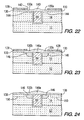
- the opening 122 through the nitride layer 128 is photolithographically enlarged to the opening 142 shown in FIG. 22 .
- N type dopant ions are then implanted through the opening 142 and through the exposed portions 130a of the oxide layer 130 (but not through the oxide cap 140) to form an N type region 144 basically identical to the N type region 74 formed through the opening 72 in FIG. 12 .
- Differences, however, are that because the oxide layer portion 130a exposed through the window 142 in FIG. 22 is thinner (as described) than the exposed oxide layer portion 68b in FIG. 12 , lower energy need be used to penetrate the oxide layer to form the implanted N type region.
- the extra thick oxide cap 140 provides even greater protection against ion implantation into the gate electrode 64 and gate oxide layer 136. Thus, an extra ion masking layer such as the cap masking layer 82a shown in FIG. 14 is not required.
- the implanted region 144 shown in FIG. 22 is then diffused to expand into contact with the gate oxide layer 138, as shown in FIG. 23 , and to form an N type source region 146.
- the portions 130a of the oxide layer 130 ( FIG. 22 ) exposed through the window 142 remain exposed and grow into greater thickness portions 130b ( FIG. 23 ) having a thickness of, for example, around 40-100 nm (400-1,000 A) (versus the thickness of around 20-40 nm (200-400 A) of the remaining portions of the oxide layer 130 covered by the nitride layer 128).
- the nitride layer 128 is then removed, as shown in FIG. 24 .
- P type dopant ions are then implanted into the workpiece with energy sufficient to penetrate only the thinnest portion of the oxide layer 130 to form a P.sup.+ region 150 spaced slightly away from the N source region 146.
- the P.sup.+ region 150 is then diffused into contact with the N region 146, thus having the appearance, as in FIG. 13 , where the P.sup.+ region 38 contacts the source region 24.
- the thickened portions 130b of the oxide layer 130 serve as a mask during the implantation of the P type dopants into the P layer 14 to form the region 150.
- a photolithographic step used in the other embodiments, e.g., to define the mask 76 shown in Fig. 13 is not required. This reduces the cost of the process.
- the second point relates to the fact that, although not illustrated, at some stage in the processing, the oxide layer 130 must be stripped to expose a surface of the silicon layer 14 for the deposition of a metal electrode thereon.
- the oxide layer 130 In the process illustrated in Figs. 19-24 , because the original oxide layer 130 ( Fig. 19 ) is protected by the silicon nitride layer 128, the oxide layer 130 remains relatively pure and uncontaminated and thus can be quite easily stripped. The result of this is that upon stripping of the oxide layer 130, the surface of the P layer 14 thus exposed is quite clean and not contaminated by the process used for stripping the oxide layer, and the metal electrode deposition step can be immediately performed without further cleaning or surface preparation processes. This is desirable as further simplifying the processing leading to reduced costs and higher yield.
- Silicon is the presently preferred semiconductor material.
- silicon dioxide is the presently preferred dielectric material used for the gate oxide and various masking layers.
- Other dielectric materials can be used, for example, "oxynitride” (silicon dioxide plus silicon nitride) or tantalum oxide.
- doped polycrystalline silicon is the preferred gate electrode material, silicides of tungsten, cobalt or titanium can be used.
- a semiconductor device a trench etched into a surface of a semiconductor body comprising, from the surface down, a highly doped first (source) region; a moderately doped second (body) region; and a lightly doped third (drain) region.
- the trench walls are then oxidized.
- the trench is first formed by etching and the trench walls then oxidized prior to the formation of the first region. Trenches having straighter walls and more uniformly thick oxides are thus formed.
Landscapes
- Insulated Gate Type Field-Effect Transistor (AREA)
- Element Separation (AREA)
Claims (7)
- Procédé de fabrication d'un dispositif MOS dans un corps (90) en silicium, le matériau de silicium comportant une première couche (12) d'un premier type de conductivité ayant une première surface et une deuxième couche (14) formant une interface avec la première surface, la deuxième couche (14) ayant une conductivité supérieure à celle de la première couche et étant d'un second type de conductivité, le procédé comprenant les étapes suivantes :graver une tranchée (56) entièrement dans la deuxième couche (14) à partir d'une première surface de celle-ci opposée à ladite interface, la tranchée (56) s'étendant à travers l'interface dans la première couche (12), la tranchée (56) ayant des parois latérales continues respectives constituées de surfaces exposées des première et deuxième couches (12, 14) ;recouvrir au moins une partie des parois latérales d'une troisième couche de dioxyde de silicium (60), ladite partie comprenant ladite interface ;recouvrir au moins une partie de la troisième couche de dioxyde de silicium avec un matériau conducteur électrique (64) ; l'étape de couverture comprenant le remplissage de la tranchée avec du polysilicium dopé ;former par croissance thermique une quatrième couche de dioxyde de silicium (68) sur des surfaces exposées dudit corps, la quatrième couche comprenant des premières parties recouvrant des parties de la première surface de la deuxième couche (14) entourant la tranchée et séparées de celle-ci par un intervalle, une deuxième partie (68a) sur la surface du matériau conducteur électrique (64) dans la tranchée, et des troisièmes parties recouvrant la troisième couche et l'intervalle, les deuxième et troisième parties étant plus épaisses que la première partie,doper une première région (96) de la deuxième couche (14) avec une conductivité du premier type et d'une troisième conductivité supérieure à la deuxième conductivité de la deuxième couche, en implantant les ions dopants avec une énergie suffisante pour passer à travers les premières parties de la quatrième couche (68) mais pas suffisante pour passer à travers les deuxième (68a) et troisième parties de la quatrième couche ; le procédé comprenant en outre une étape consistant à chauffer pour diffuser les ions implantés dans la première région (96), étendant la première région (96) en une deuxième région (96a) contactant la couche de dioxyde de silicium (60), la deuxième région (96a) étant contigüe avec la partie des parois latérales de la tranchée recouvertes de la couche de dioxyde de silicium (60) et du matériau conducteur (64), la deuxième région (96a) étant espacée dans la deuxième couche (14) par rapport à ladite interface.
- Procédé selon la revendication 1, dans lequel la concentration de la deuxième couche (14) est supérieure à celle de la première couche (12) avec un facteur d'au moins un ordre de grandeur, et la concentration de la deuxième région (96a) est supérieure à celle de la deuxième couche (14) avec un facteur d'au moins quatre ordres de grandeur.
- Procédé selon la revendication 1 ou 2, dans lequel la première surface de la deuxième couche (14) se trouve dans le plan de cristal 100, et l'étape de gravure est réalisée par un processus de gravure par ions réactifs, la paroi de la tranchée se trouvant de préférence dans le plan de cristal 110.
- Procédé selon l'une quelconque des revendications précédentes, caractérisé par le fait de prévoir, avant l'étape d'introduction de dopants, un masque impénétrable par des ions (70) comportant une ouverture exposant les première, deuxième et troisième parties de la quatrième couche (68).
- Procédé selon l'une quelconque des revendications 1 à 3, caractérisé par les étapes suivantes :prévoir un masque impénétrable par des ions (98) recouvrant les deuxième (68a) et troisième parties de la quatrième couche (68) et une première longueur de la première partie de la quatrième couche contigüe avec la troisième partie, le masque d'ions (98) exposant une deuxième longueur de la première partie de la quatrième couche (68) recouvrant une partie de la deuxième région (96a) éloignée de la tranchée (56) ;graver dans la deuxième couche (14) à travers la partie de celle-ci exposée par le masque d'ions sur une profondeur supérieure à la profondeur de la deuxième région (96a) pour exposer une deuxième surface (104) de la deuxième couche (14) ; etintroduire des seconds dopants dans la deuxième couche (14) à travers la deuxième surface pour former une troisième région (106) du deuxième type de conductivité, la troisième région (106) ayant une quatrième conductivité supérieure à la deuxième conductivité de la deuxième couche (14) et étant contigüe avec la deuxième région (96a).
- Procédé de fabrication d'un dispositif MOS dans un corps (90) en silicium, le matériau de silicium comportant une première couche (12) d'un premier type de conductivité ayant une première surface et une deuxième couche (14) formant une interface avec la première surface, la deuxième couche (14) ayant une conductivité supérieure à celle de la première couche et étant d'un deuxième type de conductivité, le procédé comprenant les étapes suivantes :former une troisième couche de dioxyde de silicium (130) sur une première surface de la deuxième couche (14) opposée à l'interface et déposer un masque impénétrable par des ions (128) ;former une ouverture (122) dans le masque (128) et dans la troisième couche (30) exposant une partie de la deuxième couche (14) opposée à ladite interface ;graver une tranchée (136) entièrement à travers la partie exposée de la deuxième couche (14), la tranchée (136) s'étendant à travers l'interface dans la première couche (12), la tranchée (136) ayant des parois latérales continues respectives constituées de surfaces exposées des première et deuxième couches (12, 14) ;recouvrir au moins une partie des parois latérales d'une quatrième couche de dioxyde de silicium (138), ladite partie comprenant ladite interface ;recouvrir au moins une partie de la quatrième couche de dioxyde de silicium avec un matériau conducteur électrique (64), l'étape de couverture comprenant le remplissage de la tranchée avec du polysilicium dopé ;former par croissance thermique une couche de couvercle en dioxyde de silicium (140) sur la surface du matériau conducteur électrique (64) et sur des parties de bords exposés de la troisième (130) et de la quatrième (138) couche avec des parties recouvrant la troisième couche et des parties adjacentes de la première surface de la deuxième couche (14), ladite couche de couvercle (140) étant plus épaisse que la troisième couche (130) ;élargir l'ouverture dans la couche de masque pour former une ouverture élargie (142) pour exposer des premières parties (130a) de la troisième couche (130) ;doper une première région (144) de la deuxième couche (14) avec une conductivité du premier type et d'une troisième conductivité supérieure à la deuxième conductivité de la deuxième couche, en implantant des ions dopants avec une énergie suffisante pour passer à travers la troisième couche (130) mais pas suffisante pour passer à travers la couche de couvercle (140) ; le procédé comprenant en outre une étape consistant à chauffer pour diffuser les ions implantés dans la première région (144), étendant la première région (144) en une deuxième région (146) contactant la quatrième couche de dioxyde de silicium (138), la deuxième région (146) étant espacée dans la deuxième couche (14) par rapport à ladite interface ;pendant ce processus de diffusion les premières parties (130a) exposées à travers l'ouverture (142) croissent en des parties plus épaisses (130b) ;puis retirer le masque (128) pour exposer des deuxièmes parties de la troisième couche (130) contigües avec les premières parties plus épaisses (130b) et ayant une épaisseur inférieure à celle des premières parties plus épaisses (130b) de la troisième couche (130) et de la couche de couvercle (140), et implanter par des ions des deuxièmes dopants avec une énergie suffisante pour pénétrer seulement à travers les deuxièmes parties de la troisième couche (130) pour former une troisième région (150) dans la deuxième couche (14) du deuxième type de conductivité, la troisième région (150) étant d'une conductivité supérieure à la deuxième conductivité de la deuxième couche (14).
- Procédé selon la revendication 4 ou 6, dans lequel le masque (70, 128) comprend du nitrure de silicium.
Applications Claiming Priority (2)
| Application Number | Priority Date | Filing Date | Title |
|---|---|---|---|
| US255092 | 1994-06-07 | ||
| US09/255,092 US6077744A (en) | 1999-02-22 | 1999-02-22 | Semiconductor trench MOS devices |
Publications (3)
| Publication Number | Publication Date |
|---|---|
| EP1032028A2 EP1032028A2 (fr) | 2000-08-30 |
| EP1032028A3 EP1032028A3 (fr) | 2003-12-03 |
| EP1032028B1 true EP1032028B1 (fr) | 2010-09-15 |
Family
ID=22966809
Family Applications (1)
| Application Number | Title | Priority Date | Filing Date |
|---|---|---|---|
| EP00102399A Expired - Lifetime EP1032028B1 (fr) | 1999-02-22 | 2000-02-03 | Dispositif MOS amélioré à tranchée |
Country Status (6)
| Country | Link |
|---|---|
| US (1) | US6077744A (fr) |
| EP (1) | EP1032028B1 (fr) |
| JP (1) | JP4833391B2 (fr) |
| KR (1) | KR100762523B1 (fr) |
| DE (1) | DE60044959D1 (fr) |
| TW (1) | TWI224834B (fr) |
Families Citing this family (7)
| Publication number | Priority date | Publication date | Assignee | Title |
|---|---|---|---|---|
| TW410382B (en) * | 1999-06-11 | 2000-11-01 | United Microelectronics Corp | Method of manufacturing forming metal oxide semiconductor transistor with raised source/drain |
| US6511883B1 (en) * | 1999-07-07 | 2003-01-28 | United Microelectronics Corp. | Method of fabricating MOS sensor |
| US6417050B1 (en) * | 2000-08-07 | 2002-07-09 | Semiconductor Components Industries Llc | Semiconductor component and method of manufacture |
| US6887768B1 (en) * | 2003-05-15 | 2005-05-03 | Lovoltech, Inc. | Method and structure for composite trench fill |
| JP2008053276A (ja) * | 2006-08-22 | 2008-03-06 | Nec Electronics Corp | 半導体装置の製造方法 |
| US7601596B2 (en) * | 2006-11-16 | 2009-10-13 | Infineon Technologies Austria Ag | Semiconductor device with trench transistors and method for manufacturing such a device |
| US8507298B2 (en) * | 2011-12-02 | 2013-08-13 | Varian Semiconductor Equipment Associates, Inc. | Patterned implant of a dielectric layer |
Family Cites Families (9)
| Publication number | Priority date | Publication date | Assignee | Title |
|---|---|---|---|---|
| JPH07273327A (ja) * | 1994-03-31 | 1995-10-20 | Nippondenso Co Ltd | 半導体装置の製造方法 |
| JP3338178B2 (ja) * | 1994-05-30 | 2002-10-28 | 株式会社東芝 | 半導体装置およびその製造方法 |
| DE4435458C2 (de) * | 1994-10-04 | 1998-07-02 | Siemens Ag | Durch Feldeffekt steuerbares Halbleiterbauelement |
| US5629543A (en) * | 1995-08-21 | 1997-05-13 | Siliconix Incorporated | Trenched DMOS transistor with buried layer for reduced on-resistance and ruggedness |
| JP3369388B2 (ja) * | 1996-01-30 | 2003-01-20 | 株式会社東芝 | 半導体装置 |
| JP3217690B2 (ja) * | 1996-03-22 | 2001-10-09 | 株式会社東芝 | 半導体装置の製造方法 |
| KR100218537B1 (ko) * | 1996-05-22 | 1999-09-01 | 김덕중 | 트렌치 확산 모스 트랜지스터의 구조 및 제조 공정 |
| JP4077529B2 (ja) * | 1996-05-22 | 2008-04-16 | フェアチャイルドコリア半導体株式会社 | トレンチ拡散mosトランジスタの製造方法 |
| JPH10270689A (ja) * | 1997-03-28 | 1998-10-09 | Hitachi Ltd | 半導体装置 |
-
1999
- 1999-02-22 US US09/255,092 patent/US6077744A/en not_active Expired - Lifetime
-
2000
- 2000-02-03 DE DE60044959T patent/DE60044959D1/de not_active Expired - Lifetime
- 2000-02-03 EP EP00102399A patent/EP1032028B1/fr not_active Expired - Lifetime
- 2000-02-17 TW TW089102707A patent/TWI224834B/zh not_active IP Right Cessation
- 2000-02-22 KR KR1020000008497A patent/KR100762523B1/ko not_active Expired - Lifetime
- 2000-02-22 JP JP2000044365A patent/JP4833391B2/ja not_active Expired - Lifetime
Also Published As
| Publication number | Publication date |
|---|---|
| TWI224834B (en) | 2004-12-01 |
| EP1032028A3 (fr) | 2003-12-03 |
| JP2000243962A (ja) | 2000-09-08 |
| KR100762523B1 (ko) | 2007-10-01 |
| EP1032028A2 (fr) | 2000-08-30 |
| JP4833391B2 (ja) | 2011-12-07 |
| KR20000062591A (ko) | 2000-10-25 |
| US6077744A (en) | 2000-06-20 |
| DE60044959D1 (de) | 2010-10-28 |
Similar Documents
| Publication | Publication Date | Title |
|---|---|---|
| CA1273128A (fr) | Methode de fabrication de dispositifs bicmos | |
| JP3416617B2 (ja) | マスク数を低減したmosゲートデバイスの製造プロセス | |
| US4417385A (en) | Processes for manufacturing insulated-gate semiconductor devices with integral shorts | |
| US4711017A (en) | Formation of buried diffusion devices | |
| EP0139371B1 (fr) | Procédé pour fabriquer un circuit intégré de type MOS utilisant une méthode pour former des couches en siliciure de métaux réfractaires | |
| US4481706A (en) | Process for manufacturing integrated bi-polar transistors of very small dimensions | |
| US4810665A (en) | Semiconductor device and method of fabrication | |
| JPH02125623A (ja) | 自己整合トランジスタの製造方法 | |
| JP2010500765A (ja) | Soi又はバルクシリコンの何れか内の内蔵バックゲートを有するjfet | |
| EP0033495B1 (fr) | Procédé de fabrication d'un transistor bipolaire à grande vitesse | |
| JPH0666325B2 (ja) | 凹状のエピタキシャル成長固有ベース領域を有する垂直バイポーラ・トランジスタ及びその製造方法 | |
| EP0242746A1 (fr) | Procédé de fabrication d'un circuit intégré | |
| US6887760B2 (en) | Fabrication process of a trench gate power MOS transistor with scaled channel | |
| US4473941A (en) | Method of fabricating zener diodes | |
| EP0519592B1 (fr) | Procédé pour fabriquer un circuit intégré monolithique, auto-aligné et planaire comportant des transistors verticaux | |
| US5106770A (en) | Method of manufacturing semiconductor devices | |
| US5952679A (en) | Semiconductor substrate and method for straightening warp of semiconductor substrate | |
| KR100272051B1 (ko) | 접점윈도우를통해베이스주입한p-채널mos게이트소자제조공정 | |
| EP0600149B1 (fr) | Méthode de fabrication d'un transistor à induction statique auto-aligné | |
| EP1032028B1 (fr) | Dispositif MOS amélioré à tranchée | |
| CA1197926A (fr) | Drain sans chevauchement et contacts auto-alignes pour dispositif mos | |
| RU1830156C (ru) | Способ изготовлени полупроводниковых приборов | |
| US6100140A (en) | Manufacturing method of semiconductor device | |
| JPH04103127A (ja) | 半導体装置の素子の分離方法 | |
| KR100305205B1 (ko) | 반도체소자의제조방법 |
Legal Events
| Date | Code | Title | Description |
|---|---|---|---|
| PUAI | Public reference made under article 153(3) epc to a published international application that has entered the european phase |
Free format text: ORIGINAL CODE: 0009012 |
|
| AK | Designated contracting states |
Kind code of ref document: A2 Designated state(s): AT BE CH CY DE DK ES FI FR GB GR IE IT LI LU MC NL PT SE |
|
| AX | Request for extension of the european patent |
Free format text: AL;LT;LV;MK;RO;SI |
|
| PUAL | Search report despatched |
Free format text: ORIGINAL CODE: 0009013 |
|
| AK | Designated contracting states |
Kind code of ref document: A3 Designated state(s): AT BE CH CY DE DK ES FI FR GB GR IE IT LI LU MC NL PT SE |
|
| AX | Request for extension of the european patent |
Extension state: AL LT LV MK RO SI |
|
| 17P | Request for examination filed |
Effective date: 20040211 |
|
| AKX | Designation fees paid |
Designated state(s): DE DK FR GB IT |
|
| 17Q | First examination report despatched |
Effective date: 20040802 |
|
| GRAP | Despatch of communication of intention to grant a patent |
Free format text: ORIGINAL CODE: EPIDOSNIGR1 |
|
| RAP1 | Party data changed (applicant data changed or rights of an application transferred) |
Owner name: FAIRCHILD SEMICONDUCTOR CORPORATION |
|
| GRAS | Grant fee paid |
Free format text: ORIGINAL CODE: EPIDOSNIGR3 |
|
| GRAA | (expected) grant |
Free format text: ORIGINAL CODE: 0009210 |
|
| AK | Designated contracting states |
Kind code of ref document: B1 Designated state(s): DE DK FR GB IT |
|
| REG | Reference to a national code |
Ref country code: GB Ref legal event code: FG4D |
|
| REF | Corresponds to: |
Ref document number: 60044959 Country of ref document: DE Date of ref document: 20101028 Kind code of ref document: P |
|
| PG25 | Lapsed in a contracting state [announced via postgrant information from national office to epo] |
Ref country code: IT Free format text: LAPSE BECAUSE OF FAILURE TO SUBMIT A TRANSLATION OF THE DESCRIPTION OR TO PAY THE FEE WITHIN THE PRESCRIBED TIME-LIMIT Effective date: 20100915 |
|
| PLBE | No opposition filed within time limit |
Free format text: ORIGINAL CODE: 0009261 |
|
| STAA | Information on the status of an ep patent application or granted ep patent |
Free format text: STATUS: NO OPPOSITION FILED WITHIN TIME LIMIT |
|
| 26N | No opposition filed |
Effective date: 20110616 |
|
| PG25 | Lapsed in a contracting state [announced via postgrant information from national office to epo] |
Ref country code: DK Free format text: LAPSE BECAUSE OF FAILURE TO SUBMIT A TRANSLATION OF THE DESCRIPTION OR TO PAY THE FEE WITHIN THE PRESCRIBED TIME-LIMIT Effective date: 20100915 |
|
| REG | Reference to a national code |
Ref country code: DE Ref legal event code: R097 Ref document number: 60044959 Country of ref document: DE Effective date: 20110616 |
|
| GBPC | Gb: european patent ceased through non-payment of renewal fee |
Effective date: 20110203 |
|
| REG | Reference to a national code |
Ref country code: FR Ref legal event code: ST Effective date: 20111102 |
|
| PG25 | Lapsed in a contracting state [announced via postgrant information from national office to epo] |
Ref country code: FR Free format text: LAPSE BECAUSE OF NON-PAYMENT OF DUE FEES Effective date: 20110228 |
|
| PG25 | Lapsed in a contracting state [announced via postgrant information from national office to epo] |
Ref country code: GB Free format text: LAPSE BECAUSE OF NON-PAYMENT OF DUE FEES Effective date: 20110203 |
|
| PGFP | Annual fee paid to national office [announced via postgrant information from national office to epo] |
Ref country code: DE Payment date: 20170119 Year of fee payment: 18 |
|
| REG | Reference to a national code |
Ref country code: DE Ref legal event code: R119 Ref document number: 60044959 Country of ref document: DE |
|
| PG25 | Lapsed in a contracting state [announced via postgrant information from national office to epo] |
Ref country code: DE Free format text: LAPSE BECAUSE OF NON-PAYMENT OF DUE FEES Effective date: 20180901 |