EP1032051A2 - Verfahren zur Herstellung einer photovoltaischen Dünnfilmvorrichtung - Google Patents
Verfahren zur Herstellung einer photovoltaischen Dünnfilmvorrichtung Download PDFInfo
- Publication number
- EP1032051A2 EP1032051A2 EP99119259A EP99119259A EP1032051A2 EP 1032051 A2 EP1032051 A2 EP 1032051A2 EP 99119259 A EP99119259 A EP 99119259A EP 99119259 A EP99119259 A EP 99119259A EP 1032051 A2 EP1032051 A2 EP 1032051A2
- Authority
- EP
- European Patent Office
- Prior art keywords
- transparent conductive
- conductive film
- back transparent
- thin film
- initial
- Prior art date
- Legal status (The legal status is an assumption and is not a legal conclusion. Google has not performed a legal analysis and makes no representation as to the accuracy of the status listed.)
- Granted
Links
Images
Classifications
-
- H—ELECTRICITY
- H10—SEMICONDUCTOR DEVICES; ELECTRIC SOLID-STATE DEVICES NOT OTHERWISE PROVIDED FOR
- H10F—INORGANIC SEMICONDUCTOR DEVICES SENSITIVE TO INFRARED RADIATION, LIGHT, ELECTROMAGNETIC RADIATION OF SHORTER WAVELENGTH OR CORPUSCULAR RADIATION
- H10F71/00—Manufacture or treatment of devices covered by this subclass
- H10F71/138—Manufacture of transparent electrodes, e.g. transparent conductive oxides [TCO] or indium tin oxide [ITO] electrodes
-
- H—ELECTRICITY
- H10—SEMICONDUCTOR DEVICES; ELECTRIC SOLID-STATE DEVICES NOT OTHERWISE PROVIDED FOR
- H10F—INORGANIC SEMICONDUCTOR DEVICES SENSITIVE TO INFRARED RADIATION, LIGHT, ELECTROMAGNETIC RADIATION OF SHORTER WAVELENGTH OR CORPUSCULAR RADIATION
- H10F10/00—Individual photovoltaic cells, e.g. solar cells
- H10F10/10—Individual photovoltaic cells, e.g. solar cells having potential barriers
- H10F10/17—Photovoltaic cells having only PIN junction potential barriers
-
- H—ELECTRICITY
- H10—SEMICONDUCTOR DEVICES; ELECTRIC SOLID-STATE DEVICES NOT OTHERWISE PROVIDED FOR
- H10F—INORGANIC SEMICONDUCTOR DEVICES SENSITIVE TO INFRARED RADIATION, LIGHT, ELECTROMAGNETIC RADIATION OF SHORTER WAVELENGTH OR CORPUSCULAR RADIATION
- H10F77/00—Constructional details of devices covered by this subclass
- H10F77/40—Optical elements or arrangements
- H10F77/42—Optical elements or arrangements directly associated or integrated with photovoltaic cells, e.g. light-reflecting means or light-concentrating means
- H10F77/48—Back surface reflectors [BSR]
-
- Y—GENERAL TAGGING OF NEW TECHNOLOGICAL DEVELOPMENTS; GENERAL TAGGING OF CROSS-SECTIONAL TECHNOLOGIES SPANNING OVER SEVERAL SECTIONS OF THE IPC; TECHNICAL SUBJECTS COVERED BY FORMER USPC CROSS-REFERENCE ART COLLECTIONS [XRACs] AND DIGESTS
- Y02—TECHNOLOGIES OR APPLICATIONS FOR MITIGATION OR ADAPTATION AGAINST CLIMATE CHANGE
- Y02E—REDUCTION OF GREENHOUSE GAS [GHG] EMISSIONS, RELATED TO ENERGY GENERATION, TRANSMISSION OR DISTRIBUTION
- Y02E10/00—Energy generation through renewable energy sources
- Y02E10/50—Photovoltaic [PV] energy
- Y02E10/52—PV systems with concentrators
-
- Y—GENERAL TAGGING OF NEW TECHNOLOGICAL DEVELOPMENTS; GENERAL TAGGING OF CROSS-SECTIONAL TECHNOLOGIES SPANNING OVER SEVERAL SECTIONS OF THE IPC; TECHNICAL SUBJECTS COVERED BY FORMER USPC CROSS-REFERENCE ART COLLECTIONS [XRACs] AND DIGESTS
- Y02—TECHNOLOGIES OR APPLICATIONS FOR MITIGATION OR ADAPTATION AGAINST CLIMATE CHANGE
- Y02E—REDUCTION OF GREENHOUSE GAS [GHG] EMISSIONS, RELATED TO ENERGY GENERATION, TRANSMISSION OR DISTRIBUTION
- Y02E10/00—Energy generation through renewable energy sources
- Y02E10/50—Photovoltaic [PV] energy
- Y02E10/548—Amorphous silicon PV cells
Definitions
- the present invention relates to a method for manufacturing a thin film photovoltaic device, and, particularly, to a method for improving the performance of a thin film photovoltaic device. It should be noted that in the present specification the terms "crystalline” and “microcrystalline” are intended to also mean partially amorphous material.
- photovoltaic devices using a semiconductor thin film have been developed extensively.
- the object of the development of these photovoltaic devices is to obtain a high quality semiconductor thin film formed on an inexpensive substrate in a low temperature process which affords the compatibility of low manufacturing costs with a high performance.
- Such a photovoltaic device is expected to be used in various applications such as solar cells and photo-sensors.
- the photovoltaic device As an example of the photovoltaic device, a device in which a transparent conductive film, a thin film photovoltaic unit, a back transparent conductive film and a back metal electrode are successively laminated on a substrate has been known.
- the back transparent conductive film arranged between the thin film photovoltaic unit and the back metal electrode is formed to remove thermal strain caused by a difference in the coefficient of thermal expansion between the semiconductor thin film and the metal electrode thereby increasing the adhesion strength of the metal electrode to the thin film photovoltaic unit.
- the back transparent conductive film is formed also to prevent metal atoms of the metal electrode from diffusing into the photovoltaic unit. It is generally required for this back transparent conductive film to have a thickness of 10 nm to 1 ⁇ m with high transmittance and a low resistance as low as 1.5 ⁇ 10 -3 ⁇ cm or less.
- the back transparent conductive film which meets such requirements has been formed, for example, by sputtering under conditions of a pressure of 2 ⁇ 10 -2 Torr or less, a substrate temperature of 100 to 450°C and a discharge power of 500 to 1500 mW/cm 2 .
- the resulting photovoltaic device is not sufficiently improved in the photovoltaic characteristics when the back transparent conductive film is formed under the sputtering conditions as aforementioned.
- An object of the present invention is to provide a method for easily manufacturing a thin film photovoltaic device improved in photovoltaic characteristics.
- the present inventors have made it clear that if the back transparent conductive film is formed under the above described conventionally used sputtering conditions, the photovoltaic unit is damaged by negative ions (e.g., O - ) produced during sputtering. Specifically, the surface of the photovoltaic unit is oxidized with the result that the photovoltaic characteristics of the resulting photovoltaic device cannot be sufficiently improved.
- negative ions e.g., O -
- the present inventors have found that excellent photovoltaic characteristics can be obtained if the back transparent conductive film is formed on the photovoltaic unit by sputtering comprising steps of forming an initial thin back transparent conductive film under a low damage condition only at the initial stage and thereafter forming a main back transparent conductive film with the remainder thickness under conditions ensuring that a high quality film is obtained.
- a method for manufacturing a thin film photovoltaic device comprising a transparent conductive film, a thin film photovoltaic unit, and a back transparent conductive film and a back metal electrode which are successively formed on a substrate, wherein the back transparent conductive film is formed by sputtering comprising steps of forming an initial back transparent conductive film under a pressure of 5 ⁇ 10 -2 Torr or more for 1 to 30 seconds in the initial stage and forming a main back transparent conductive film having the remainder thickness under a pressure reduced to 1/10 the initial pressure or less.
- a method for manufacturing a thin film photovoltaic device comprising a transparent conductive film, a thin film photovoltaic unit, and a back transparent conductive film and a back metal electrode which are successively formed on a substrate, wherein the back transparent conductive film is formed by sputtering comprising steps of forming an initial back transparent conductive film at a discharge power of 80 to 500 mW/cm 2 for 1 to 30 seconds in the initial stage and forming a main back transparent conductive film having the remainder thickness at a discharge power increased to 4 times the initial discharge power or more.
- a method for manufacturing a thin film photovoltaic device comprising a transparent conductive film, a thin film photovoltaic unit, and a back transparent conductive film and a back metal electrode which are successively formed on a substrate, wherein the back transparent conductive film is formed by sputtering comprising steps of forming an initial back transparent conductive film at a temperature of 100°C or less for 1 to 30 seconds in the initial stage and forming a main back transparent conductive film having the remainder thickness at a temperature of 100°C or more.
- a material of the back transparent conductive film is not particularly limited as long as it is a transparent conductive oxide (TCO), it is preferable to use a film comprising primarily ZnO.
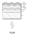
- FIGURE is a sectional view showing an embodiment of a silicon-based thin film photovoltaic device according to the present invention.
- examples of the photovoltaic unit include a photovoltaic unit containing an amorphous silicon-based photovoltaic layer, a photovoltaic unit containing a crystalline silicon-based photovoltaic layer, a tandem-type photovoltaic unit produced by laminating one or more amorphous silicon-based photovoltaic layers and one or more crystalline silicon-based photovoltaic layers, a photovoltaic unit containing a CdS/CdTe-based photovoltaic layer and a photovoltaic unit containing a CuInS 2 -based photovoltaic layer.
- the present invention will be hereinafter explained in more detail with the silicon-based thin film photovoltaic unit as an example.
- the silicon-based thin film photovoltaic device has a structure in which a transparent conductive film 2, a photovoltaic unit consisting of first conductivity-type layer (e.g., a p-type layer) 111, a photoelectric conversion layer 112 comprising substantially an intrinsic semiconductor, and an opposite conductivity-type (e.g., an n-type layer) 113 and a composite electrode 21 consisting of a back transparent conductive film 211 and a back metal electrode 212 are successively laminated on a substrate 1.
- a light h ⁇ to be subjected to photoelectric conversion is introduced from the side of the substrate 1.
- the substrate 1 can be a transparent substrate made of, for example, an organic film, ceramics, or an inexpensive glass having low melting point.
- the transparent conductive film 2 disposed on the substrate 1 can be a transparent conductive film containing one or more layers of compounds selected from the group consisting of ITO, SnO 2 and ZnO. Among these compounds, SnO 2 is particularly preferable in view of transparency, conductivity and chemical stability. ITO is also preferable in view of processability, conductivity and transmittance.
- the transparent conductive film can be formed on the substrate 1 by vacuum deposition, thermal CVD or sputtering.
- the photovoltaic unit 11 is then formed on the transparent conductive film 2.
- the photovoltaic unit 11 may be either an amorphous silicon-based or a crystalline (polycrystalline or microcrystalline) silicon-based.
- FIGURE shows an example in which the photovoltaic unit 11 of an amorphous silicon-based is formed.
- All semiconductor layers in the photovoltaic unit 11 can be deposited by a plasma CVD method in which the substrate temperature is set at 400°C or less.
- a plasma CVD method a generally well-known parallel plate type 13.56 MHz RF plasma CVD method or a plasma CVD method making use of a high frequency power source ranging from the RF zone frequency of 150 MHz or less to the VHF zone may be used.
- the photovoltaic unit 11 comprises the first conductivity-type layer 111, the photoelectric conversion layer 112 and the opposite conductivity-type layer 113.
- the first conductivity-type layer 111 may be either a p-type layer or an n-type layer.
- the opposite conductivity-type layer 113 may be an n-type layer or a p-type layer.
- the photoelectric conversion layer 112 comprises substantially a non-doped intrinsic semiconductor. It is noted that a p-type layer is generally disposed on the incident side of light on a photovoltaic device and hence the first conductivity-type layer 111 is a p-type layer and the opposite conductivity-type layer 113 is an n-type layer in the structure shown in FIGURE.
- the first conductivity-type layer 111 comprises a p-type silicon thin film which is doped with, for example, boron as an conductivity-type determining impurity.
- impurity there is no limitation to the impurity, and aluminum may be used in the case of a p-type layer.
- a material for the first conductivity-type layer 111 amorphous silicon, an alloy material such as amorphous silicon carbide or amorphous silicon germanium, polycrystalline silicon or microcrystalline silicon partially containing amorphous silicon or its alloy material may be used.
- the deposited first conductivity-type layer 111 may be irradiated with pulse laser light (laser annealing) to control the crystallinity and the carrier density.
- the photoelectric conversion layer 112 is deposited on the first conductivity-type layer 111.
- the photoelectric conversion layer 112 comprises substantially a non-doped intrinsic semiconductor. It may be an amorphous silicon-based or a crystalline (polycrystalline or microcrystalline) silicon-based. There is no particular limitation to a semiconductor material constituting the photoelectric conversion layer 112, and an alloy material such as silicon carbide or silicon germanium may be used.
- the thickness of the photoelectric conversion layer 112 is generally 0.3 to 0.4 ⁇ m in the case of an amorphous silicon-based and 0.5 to 20 ⁇ m in the case of a crystalline silicon-based to obtain a necessary and sufficient photoelectric conversion.
- crystalline (polycrystalline or microcrystalline) silicon-based photoelectric conversion layer a layer of polycrystalline or microcrystalline silicon with an at least 80% crystallized volume fraction or a layer of weak p- or n-type crystalline silicon containing a small amount of impurity and having sufficient photoelectric conversion efficiency can be used.
- the opposite conductivity-type layer 113 comprises, for example, an n-type silicon thin film which is doped with phosphorus as an conductivity determining impurity.
- the impurity and nitrogen or the like may be used in an n-type layer.
- the semiconductor materials for the opposite conductivity-type layer 113 and amorphous silicon, an alloy material such as amorphous silicon carbide or amorphous silicon germanium, polycrystalline silicon or microcrystalline silicon partially containing amorphous silicon or its alloy material may be used.
- a composite electrode 21 containing a back transparent conductive film 211 and a back metal electrode 212 is formed.
- the functions of the back transparent conductive film 211 are to increase the adhesion strength of the back metal electrode 212 to the photovoltaic unit 11, to improve the reflecting efficiency of the back metal electrode 212 and to prevent the photovoltaic unit 11 from being chemically changed.
- the back transparent conductive film 211 is preferably formed of at least one material selected from transparent conductive oxides (TCO) such as ITO, SnO 2 and ZnO.
- TCO transparent conductive oxides
- a film comprising ZnO as a major component is particularly preferable. It is preferable that the thickness of the back transparent conductive film 211 comprising ZnO as a major component be 10 nm to 1 ⁇ m and the specific resistance be 1.5 ⁇ 10 -3 ⁇ cm or less.
- the back transparent conductive film is formed by sputtering under a low damage condition, thereby suppressing a damage to the photovoltaic unit which is caused by negative ions (e.g., an O - ion) produced during sputtering and reducing oxidation of the surface of the photovoltaic unit.
- negative ions e.g., an O - ion
- the low damage condition brings about the back transparent conductive film having impaired quality (resistance, transmittance) while the photovoltaic characteristics are not improved.
- an initial thin back transparent conductive film is formed on the surface of the photovoltaic unit under a low damage condition only in the initial stage and thereafter a main back transparent conductive film is formed under the condition ensuring that a high quality film can be obtained, thereby reducing a damage to the photovoltaic unit and improving the photovoltaic characteristics of a finally produced photovoltaic device.
- Specific deposition methods for forming the back transparent conductive film by sputtering include the following methods (1) to (3).
- a film is formed under the initial condition (low damage condition) for 1 to 30 seconds to form an initial back transparent conductive film with a thickness of 1 to 10 nm. Since the sputtering conditions can easily be switched from the initial condition (low damage condition) to the second stage condition (high quality film-forming condition), there is no difference in the workability between the conventional manufacturing method and the manufacturing method of the present invention. It is needless to say that the back transparent conductive film may be formed in a combination of the above three methods.
- the back metal electrode 212 may be formed by using a method such as vacuum deposition and sputtering.
- the back metal electrode 212 is preferably formed by using one metal selected from the group consisting of Ag, Au, Al, Cu and Pt or alloys containing these metals.
- the amorphous silicon-based photovoltaic device shown in FIGURE was produced. Firstly, a transparent conductive film 2 comprising SnO 2 was formed on a glass substrate 1. On the transparent conductive film 2, an amorphous silicon-based photovoltaic unit 11 containing first conductivity-type layer (p-type layer) 111, an amorphous silicon-based photoelectric conversion layer (i-type layer) 112 and an opposite conductivity-type layer (n-type layer) 113 was formed by a plasma CVD method. On the photovoltaic unit 11, a composite electrode 21 consisting of a back transparent conductive film 211 comprising 90 nm-thick ZnO doped with Al and a back metal electrode 212 comprising Ag was formed by sputtering.
- the above back transparent conductive film 211 was deposited by using RF magnetron sputtering under two-stage condition shown below.
- Ar gas was used as the sputtering gas and the temperature and the RF power density were not changed but kept at a constant temperature of 150°C and a constant RF power density of 850 mW/cm 2 , respectively.
- sputtering was continued for 10 seconds under a chamber pressure of 1 ⁇ 10 -1 Torr to form an initial ZnO film with a thickness of about 2 nm. Then, the pressure was reduced to 3 ⁇ 10 -3 Torr to form a main ZnO film with the remainder thickness.
- the photovoltaic device shown in FIGURE was manufactured in the same manner as in Example 1 except that the pressure was set at a constant chamber pressure of 3 ⁇ 10 -3 Torr when the back transparent conductive film 211 is formed by sputtering.
- Example 2 The same procedures as in Example 1 were carried out, except that a back transparent conductive film 211 was formed under two-stage condition shown below.
- Ar gas was used as the sputtering gas and the substrate temperature and the chamber pressure were not changed but kept at a constant temperature of 150°C and a constant pressure of 3 ⁇ 10 -3 Torr, respectively.
- sputtering was continued for 10 seconds at an RF power density of 200 mW/cm 2 to form an initial ZnO film with a thickness of about 2 nm. Then, the RF power density was raised to 850 mW/cm 2 to form a main ZnO film with the remainder thickness.
- Example 2 The same procedures as in Example 1 were carried out, except that a back transparent conductive film 211 was formed under two-stage condition shown below.
- Ar gas was used as the sputtering gas and the pressure and the RF power density were not changed but kept at a constant pressure of 3 ⁇ 10 -3 Torr and a constant RF power density of 850 mW/cm 2 , respectively.
- sputtering was continued for 10 seconds at a substrate temperature of 50°C to form an initial ZnO film with a thickness of about 2 nm. Then, the substrate temperature was raised to 150°C to form a main ZnO film with the remainder thickness.
Landscapes
- Photovoltaic Devices (AREA)
- Physical Vapour Deposition (AREA)
Applications Claiming Priority (2)
| Application Number | Priority Date | Filing Date | Title |
|---|---|---|---|
| JP11050587A JP3056200B1 (ja) | 1999-02-26 | 1999-02-26 | 薄膜光電変換装置の製造方法 |
| JP5058799 | 1999-02-26 |
Publications (3)
| Publication Number | Publication Date |
|---|---|
| EP1032051A2 true EP1032051A2 (de) | 2000-08-30 |
| EP1032051A3 EP1032051A3 (de) | 2003-06-18 |
| EP1032051B1 EP1032051B1 (de) | 2009-11-25 |
Family
ID=12863118
Family Applications (1)
| Application Number | Title | Priority Date | Filing Date |
|---|---|---|---|
| EP99119259A Expired - Lifetime EP1032051B1 (de) | 1999-02-26 | 1999-09-28 | Verfahren zur Herstellung einer photovoltaischen Dünnschichtvorrichtung |
Country Status (6)
| Country | Link |
|---|---|
| US (1) | US6187150B1 (de) |
| EP (1) | EP1032051B1 (de) |
| JP (1) | JP3056200B1 (de) |
| AT (1) | ATE450056T1 (de) |
| AU (1) | AU761469B2 (de) |
| DE (1) | DE69941675D1 (de) |
Cited By (17)
| Publication number | Priority date | Publication date | Assignee | Title |
|---|---|---|---|---|
| WO2008150769A3 (en) * | 2007-05-31 | 2010-07-22 | Thinsilicon Corporation | Photovoltaic device and method of manufacturing photovoltaic devices |
| WO2011019886A1 (en) | 2009-08-13 | 2011-02-17 | Dow Global Technologies, Inc. | A multi-layer laminate structure and manufacturing method |
| DE102009051345A1 (de) * | 2009-10-30 | 2011-05-12 | Fraunhofer-Gesellschaft zur Förderung der angewandten Forschung e.V. | Anordnung umfassend eine transparente elektrisch leitfähige Schicht, Anordnung umfassend eine photoelektrische Vorrichtung und Verfahren zur Herstellung einer transparenten Elektrode |
| WO2011056921A1 (en) | 2009-11-04 | 2011-05-12 | Dow Global Technologies Llc | Building integrated photovoltaic having injection molded component |
| WO2011112759A2 (en) | 2010-03-12 | 2011-09-15 | Dow Global Technologies Llc | Improved photovoltaic device |
| WO2012033657A2 (en) | 2010-09-07 | 2012-03-15 | Dow Global Technologies Llc | Improved photovoltaic cell assembly |
| WO2012037191A2 (en) | 2010-09-17 | 2012-03-22 | Dow Global Technologies Llc | Improved photovoltaic cell assembly and method |
| WO2012044762A1 (en) | 2010-09-30 | 2012-04-05 | Dow Global Technologies Llc | An improved connector and electronic circuit assembly for improved wet insulation resistance |
| WO2012082608A2 (en) | 2010-12-17 | 2012-06-21 | Dow Global Technologies Llc | Improved photovoltaic device |
| WO2012082604A1 (en) | 2010-12-17 | 2012-06-21 | Dow Global Technologies Llc | Improved photovoltaic device |
| WO2012082613A2 (en) | 2010-12-17 | 2012-06-21 | Dow Global Technologies Llc | Improved photovoltaic device |
| WO2012129355A2 (en) | 2011-03-22 | 2012-09-27 | Dow Global Technologies Llc | Improved photovoltaic building sheathing element with anti-slide features |
| WO2012129356A2 (en) | 2011-03-22 | 2012-09-27 | Dow Global Technologies Llc | Improved photovoltaic sheathing element with one or more tabs |
| WO2012154307A2 (en) | 2011-03-22 | 2012-11-15 | Dow Global Technologies Llc | Improved photovoltaic sheathing element with a flexible connector assembly |
| WO2015199857A1 (en) | 2014-06-26 | 2015-12-30 | Dow Global Technologies Llc | Photovoltaic devices with sealant layer and laminate assembly for improved wet insulation resistance |
| EP2999009A1 (de) | 2008-05-05 | 2016-03-23 | Dow Global Technologies LLC | Fotovoltaische vorrichtungsanordnung und verfahren |
| US9537033B2 (en) | 2011-07-29 | 2017-01-03 | Dow Global Technologies Llc | Interface system and method for photovoltaic cladding to standard cladding |
Families Citing this family (35)
| Publication number | Priority date | Publication date | Assignee | Title |
|---|---|---|---|---|
| US6500690B1 (en) * | 1999-10-27 | 2002-12-31 | Kaneka Corporation | Method of producing a thin-film photovoltaic device |
| JP2001189478A (ja) * | 1999-12-28 | 2001-07-10 | Sanyo Electric Co Ltd | 半導体素子及びその製造方法 |
| TWI234027B (en) * | 2000-06-14 | 2005-06-11 | Hannstar Display Corp | Liquid crystal display device |
| US6683275B2 (en) * | 2000-06-23 | 2004-01-27 | Memex Optical Media Solutions Ag | Method and apparatus for fabricating phase-change recording medium |
| US6908782B2 (en) * | 2000-08-18 | 2005-06-21 | Midwest Research Instittue | High carrier concentration p-type transparent conducting oxide films |
| JP2002134772A (ja) * | 2000-10-24 | 2002-05-10 | Canon Inc | シリコン系薄膜及び光起電力素子 |
| US7517784B2 (en) * | 2001-08-17 | 2009-04-14 | Alliance For Sustainable Energy, Llc | Method for producing high carrier concentration p-Type transparent conducting oxides |
| JP2003264307A (ja) * | 2002-03-11 | 2003-09-19 | Sharp Corp | 薄膜太陽電池及びその製造方法 |
| US20080213570A1 (en) * | 2007-02-16 | 2008-09-04 | Jennifer Hoyt Lalli | Self-assembled conductive deformable films |
| US20080261044A1 (en) * | 2003-02-10 | 2008-10-23 | Jennifer Hoyt Lalli | Rapidly self-assembled thin films and functional decals |
| US20080182099A1 (en) * | 2006-11-17 | 2008-07-31 | Jennifer Hoyt Lalli | Robust electrodes for shape memory films |
| US20090087348A1 (en) * | 2007-02-16 | 2009-04-02 | Richard Otto Claus | Sensor applications |
| US20050000565A1 (en) * | 2003-05-22 | 2005-01-06 | Tingying Zeng | Self-assembly methods for the fabrication of McFarland-Tang photovoltaic devices |
| JP2005050905A (ja) * | 2003-07-30 | 2005-02-24 | Sharp Corp | シリコン薄膜太陽電池の製造方法 |
| FR2900052B1 (fr) * | 2006-04-19 | 2011-02-18 | Galderma Sa | Composition comprenant au moins une phase aqueuse et au moins une phase grasse comprenant de l'ivermectine |
| US7998313B2 (en) * | 2006-12-07 | 2011-08-16 | Georgia-Pacific Consumer Products Lp | Inflated fibers of regenerated cellulose formed from ionic liquid/cellulose dope and related products |
| US20080179762A1 (en) * | 2007-01-25 | 2008-07-31 | Au Optronics Corporation | Layered structure with laser-induced aggregation silicon nano-dots in a silicon-rich dielectric layer, and applications of the same |
| US20080206550A1 (en) * | 2007-02-26 | 2008-08-28 | Michael Jeremiah Borlner | Hydrophobic surface |
| FR2914501B1 (fr) * | 2007-03-28 | 2009-12-04 | Commissariat Energie Atomique | Dispositif photovoltaique a structure a heterojonctions interdigitee discontinue |
| US20090035513A1 (en) * | 2007-03-28 | 2009-02-05 | Michael Jeremiah Bortner | Tethered nanorods |
| US20080245413A1 (en) * | 2007-04-04 | 2008-10-09 | Hang Ruan | Self assembled photovoltaic devices |
| KR101358864B1 (ko) * | 2007-07-10 | 2014-02-06 | 주성엔지니어링(주) | 태양 전지 및 이의 제조 방법 |
| US20090104434A1 (en) * | 2007-10-17 | 2009-04-23 | Jennifer Hoyt Lalli | Conformal multifunctional coatings |
| US20090104438A1 (en) * | 2007-10-17 | 2009-04-23 | Jennifer Hoyt Lalli | Abrasion resistant coatings |
| US8263852B2 (en) * | 2008-06-23 | 2012-09-11 | Atomic Energy Council—Institute of Nuclear Energy Research | Insulating device of concentration photovoltaic heat sink |
| US8445394B2 (en) | 2008-10-06 | 2013-05-21 | Corning Incorporated | Intermediate thermal expansion coefficient glass |
| US8975199B2 (en) | 2011-08-12 | 2015-03-10 | Corsam Technologies Llc | Fusion formable alkali-free intermediate thermal expansion coefficient glass |
| EP2180526A2 (de) * | 2008-10-23 | 2010-04-28 | Samsung Electronics Co., Ltd. | Photovoltaikvorrichtung und Verfahren zu deren Herstellung |
| JP5379845B2 (ja) * | 2009-03-02 | 2013-12-25 | 株式会社カネカ | 薄膜太陽電池モジュール |
| US8418418B2 (en) | 2009-04-29 | 2013-04-16 | 3Form, Inc. | Architectural panels with organic photovoltaic interlayers and methods of forming the same |
| CN102484115B (zh) * | 2009-06-30 | 2016-08-31 | Lg伊诺特有限公司 | 太阳能电池设备 |
| US20110155246A1 (en) * | 2009-12-29 | 2011-06-30 | Chih-Hung Yeh | Thin film solar cell and manufacturing method thereof |
| WO2011162940A2 (en) * | 2010-06-24 | 2011-12-29 | Applied Materials, Inc. | Method of using silicon alloy layers in thin-film photovoltaics |
| US20120318352A1 (en) * | 2011-06-14 | 2012-12-20 | General Electric Company | Photovoltaic device with reflection enhancing layer |
| US9988707B2 (en) | 2014-05-30 | 2018-06-05 | Ppg Industries Ohio, Inc. | Transparent conducting indium doped tin oxide |
Family Cites Families (11)
| Publication number | Priority date | Publication date | Assignee | Title |
|---|---|---|---|---|
| CA1184877A (en) * | 1982-05-12 | 1985-04-02 | James B. Webb | Method and apparatus for depositing conducting oxide on a substrate |
| JPH0772346B2 (ja) * | 1989-03-03 | 1995-08-02 | 日本真空技術株式会社 | 低抵抗透明導電膜の製造方法 |
| US5078804A (en) * | 1989-06-27 | 1992-01-07 | The Boeing Company | I-III-VI2 based solar cell utilizing the structure CuInGaSe2 CdZnS/ZnO |
| US5078803A (en) * | 1989-09-22 | 1992-01-07 | Siemens Solar Industries L.P. | Solar cells incorporating transparent electrodes comprising hazy zinc oxide |
| JP2788799B2 (ja) | 1991-06-28 | 1998-08-20 | キヤノン株式会社 | 太陽電池 |
| AU650782B2 (en) * | 1991-09-24 | 1994-06-30 | Canon Kabushiki Kaisha | Solar cell |
| JP2908616B2 (ja) | 1991-09-24 | 1999-06-21 | キヤノン株式会社 | 太陽電池 |
| JP2908617B2 (ja) | 1991-09-24 | 1999-06-21 | キヤノン株式会社 | 太陽電池 |
| JPH08170171A (ja) * | 1994-12-17 | 1996-07-02 | Aneruba Kk | Ito透明導電膜の作製方法 |
| JPH10144944A (ja) * | 1996-09-12 | 1998-05-29 | Canon Inc | 光起電力素子 |
| JP3527815B2 (ja) * | 1996-11-08 | 2004-05-17 | 昭和シェル石油株式会社 | 薄膜太陽電池の透明導電膜の製造方法 |
-
1999
- 1999-02-26 JP JP11050587A patent/JP3056200B1/ja not_active Expired - Fee Related
- 1999-09-28 DE DE69941675T patent/DE69941675D1/de not_active Expired - Lifetime
- 1999-09-28 EP EP99119259A patent/EP1032051B1/de not_active Expired - Lifetime
- 1999-09-28 AT AT99119259T patent/ATE450056T1/de not_active IP Right Cessation
- 1999-10-01 AU AU52592/99A patent/AU761469B2/en not_active Ceased
- 1999-10-07 US US09/414,092 patent/US6187150B1/en not_active Expired - Lifetime
Cited By (28)
| Publication number | Priority date | Publication date | Assignee | Title |
|---|---|---|---|---|
| WO2008150769A3 (en) * | 2007-05-31 | 2010-07-22 | Thinsilicon Corporation | Photovoltaic device and method of manufacturing photovoltaic devices |
| EP2999009A1 (de) | 2008-05-05 | 2016-03-23 | Dow Global Technologies LLC | Fotovoltaische vorrichtungsanordnung und verfahren |
| WO2011019886A1 (en) | 2009-08-13 | 2011-02-17 | Dow Global Technologies, Inc. | A multi-layer laminate structure and manufacturing method |
| DE102009051345A1 (de) * | 2009-10-30 | 2011-05-12 | Fraunhofer-Gesellschaft zur Förderung der angewandten Forschung e.V. | Anordnung umfassend eine transparente elektrisch leitfähige Schicht, Anordnung umfassend eine photoelektrische Vorrichtung und Verfahren zur Herstellung einer transparenten Elektrode |
| DE102009051345B4 (de) * | 2009-10-30 | 2013-07-25 | Fraunhofer-Gesellschaft zur Förderung der angewandten Forschung e.V. | Verfahren zur Herstellung einer transparenten Elektrode |
| WO2011051050A3 (de) * | 2009-10-30 | 2012-06-14 | Schüco Tf Gmbh & Co. Kg | Anordnung umfassend eine transparente elektrisch leitfähige schicht, anordnung umfassend eine photoelektrische vorrichtung und verfahren zur herstellung einer transparenten elektrode |
| CN103081113A (zh) * | 2009-10-30 | 2013-05-01 | 旭格门窗有限公司 | 包括透明导电层的装置,包括光电设备的装置和用于制造透明电极的方法 |
| WO2011056921A1 (en) | 2009-11-04 | 2011-05-12 | Dow Global Technologies Llc | Building integrated photovoltaic having injection molded component |
| WO2011112759A2 (en) | 2010-03-12 | 2011-09-15 | Dow Global Technologies Llc | Improved photovoltaic device |
| US8912426B2 (en) | 2010-03-12 | 2014-12-16 | Dow Global Technologies Llc | Photovoltaic device |
| WO2012033657A2 (en) | 2010-09-07 | 2012-03-15 | Dow Global Technologies Llc | Improved photovoltaic cell assembly |
| US9147788B2 (en) | 2010-09-07 | 2015-09-29 | Dow Global Technologies Llc | Photovoltaic cell assembly |
| WO2012037191A2 (en) | 2010-09-17 | 2012-03-22 | Dow Global Technologies Llc | Improved photovoltaic cell assembly and method |
| US9398712B2 (en) | 2010-09-30 | 2016-07-19 | Dow Global Technologies Llc | Connector and electronic circuit assembly for improved wet insulation resistance |
| WO2012044762A1 (en) | 2010-09-30 | 2012-04-05 | Dow Global Technologies Llc | An improved connector and electronic circuit assembly for improved wet insulation resistance |
| WO2012082613A2 (en) | 2010-12-17 | 2012-06-21 | Dow Global Technologies Llc | Improved photovoltaic device |
| US9602046B2 (en) | 2010-12-17 | 2017-03-21 | Dow Global Technologies Llc | Photovoltaic device |
| WO2012082604A1 (en) | 2010-12-17 | 2012-06-21 | Dow Global Technologies Llc | Improved photovoltaic device |
| WO2012082608A2 (en) | 2010-12-17 | 2012-06-21 | Dow Global Technologies Llc | Improved photovoltaic device |
| US9048358B2 (en) | 2010-12-17 | 2015-06-02 | Dow Global Technologies Llc | Photovoltaic device |
| WO2012154307A2 (en) | 2011-03-22 | 2012-11-15 | Dow Global Technologies Llc | Improved photovoltaic sheathing element with a flexible connector assembly |
| US9130091B2 (en) | 2011-03-22 | 2015-09-08 | Dow Global Technologies Llc | Photovoltaic building sheathing element with anti-slide features |
| US9391223B2 (en) | 2011-03-22 | 2016-07-12 | Dow Global Technologies Llc | Photovoltaic sheathing element with a flexible connector assembly |
| WO2012129356A2 (en) | 2011-03-22 | 2012-09-27 | Dow Global Technologies Llc | Improved photovoltaic sheathing element with one or more tabs |
| US9564545B2 (en) | 2011-03-22 | 2017-02-07 | Dow Global Technologies Llc | Photovoltaic sheathing element with one or more tabs |
| WO2012129355A2 (en) | 2011-03-22 | 2012-09-27 | Dow Global Technologies Llc | Improved photovoltaic building sheathing element with anti-slide features |
| US9537033B2 (en) | 2011-07-29 | 2017-01-03 | Dow Global Technologies Llc | Interface system and method for photovoltaic cladding to standard cladding |
| WO2015199857A1 (en) | 2014-06-26 | 2015-12-30 | Dow Global Technologies Llc | Photovoltaic devices with sealant layer and laminate assembly for improved wet insulation resistance |
Also Published As
| Publication number | Publication date |
|---|---|
| US6187150B1 (en) | 2001-02-13 |
| JP3056200B1 (ja) | 2000-06-26 |
| ATE450056T1 (de) | 2009-12-15 |
| EP1032051A3 (de) | 2003-06-18 |
| EP1032051B1 (de) | 2009-11-25 |
| JP2000252498A (ja) | 2000-09-14 |
| AU761469B2 (en) | 2003-06-05 |
| AU5259299A (en) | 2000-08-31 |
| DE69941675D1 (de) | 2010-01-07 |
Similar Documents
| Publication | Publication Date | Title |
|---|---|---|
| EP1032051B1 (de) | Verfahren zur Herstellung einer photovoltaischen Dünnschichtvorrichtung | |
| US9130074B2 (en) | High-efficiency solar cell structures and methods of manufacture | |
| US20010054436A1 (en) | Photovoltaic element, producing method therefor, and solar cell modules | |
| AU2257200A (en) | Method of producing a thin-film photovoltaic device | |
| US20080153280A1 (en) | Reactive sputter deposition of a transparent conductive film | |
| WO2008057202A1 (en) | Front electrode with thin metal film layer and high work-function buffer layer for use in photovoltaic device and method of making same | |
| US20100269897A1 (en) | Photovoltaic device and process for producing same | |
| EP0749161B1 (de) | Integriertes Dünnschicht-Sonnenzellenmodul und Herstellungsverfahren | |
| EP1160877A2 (de) | Photovoltaisches Bauelement und Herstellungsverfahren | |
| WO2011056206A2 (en) | High haze transparent contact including insertion layer for solar cells, and/or method of making the same | |
| KR20010051955A (ko) | 반도체 장치 및 그 제조 방법 | |
| US20100229934A1 (en) | Solar cell and method for the same | |
| JPH05110125A (ja) | 光起電力素子 | |
| US6252157B1 (en) | Amorphous silicon-based thin film photovoltaic device | |
| KR20140001838A (ko) | 투명 도전막 적층체 및 그 제조 방법, 그리고 박막 태양 전지 및 그 제조 방법 | |
| EP1408558B1 (de) | Fotoelektrische Umwandlungsvorrichtung | |
| JP5056651B2 (ja) | 薄膜太陽電池及び薄膜太陽電池用表面電極 | |
| JP5093502B2 (ja) | 薄膜太陽電池及び薄膜太陽電池用表面電極 | |
| JP3419108B2 (ja) | 薄膜太陽電池の製造方法 | |
| KR101783784B1 (ko) | 태양전지 모듈 및 그의 제조방법 | |
| JP2000252497A (ja) | 薄膜光電変換装置の製造方法 | |
| JP2003008036A (ja) | 太陽電池及びその製造方法 | |
| JPH10144942A (ja) | 非晶質半導体太陽電池 | |
| JP2001127316A (ja) | 薄膜光電変換装置 | |
| JP2000252499A (ja) | 薄膜光電変換装置の製造方法 |
Legal Events
| Date | Code | Title | Description |
|---|---|---|---|
| PUAI | Public reference made under article 153(3) epc to a published international application that has entered the european phase |
Free format text: ORIGINAL CODE: 0009012 |
|
| AK | Designated contracting states |
Kind code of ref document: A2 Designated state(s): AT BE CH CY DE DK ES FI FR GB GR IE IT LI LU MC NL PT SE |
|
| AX | Request for extension of the european patent |
Free format text: AL;LT;LV;MK;RO;SI |
|
| RIC1 | Information provided on ipc code assigned before grant |
Ipc: 7H 01L 31/052 B Ipc: 7H 01L 31/0392 B Ipc: 7H 01L 31/18 A |
|
| PUAL | Search report despatched |
Free format text: ORIGINAL CODE: 0009013 |
|
| AK | Designated contracting states |
Designated state(s): AT BE CH CY DE DK ES FI FR GB GR IE IT LI LU MC NL PT SE |
|
| AX | Request for extension of the european patent |
Extension state: AL LT LV MK RO SI |
|
| 17P | Request for examination filed |
Effective date: 20031121 |
|
| AKX | Designation fees paid |
Designated state(s): AT BE CH CY DE DK ES FI FR GB GR IE IT LI LU MC NL PT SE |
|
| 17Q | First examination report despatched |
Effective date: 20070322 |
|
| GRAP | Despatch of communication of intention to grant a patent |
Free format text: ORIGINAL CODE: EPIDOSNIGR1 |
|
| GRAS | Grant fee paid |
Free format text: ORIGINAL CODE: EPIDOSNIGR3 |
|
| GRAA | (expected) grant |
Free format text: ORIGINAL CODE: 0009210 |
|
| AK | Designated contracting states |
Kind code of ref document: B1 Designated state(s): AT BE CH CY DE DK ES FI FR GB GR IE IT LI LU MC NL PT SE |
|
| REG | Reference to a national code |
Ref country code: GB Ref legal event code: FG4D |
|
| REG | Reference to a national code |
Ref country code: CH Ref legal event code: EP |
|
| REG | Reference to a national code |
Ref country code: IE Ref legal event code: FG4D |
|
| REF | Corresponds to: |
Ref document number: 69941675 Country of ref document: DE Date of ref document: 20100107 Kind code of ref document: P |
|
| REG | Reference to a national code |
Ref country code: NL Ref legal event code: VDEP Effective date: 20091125 |
|
| PG25 | Lapsed in a contracting state [announced via postgrant information from national office to epo] |
Ref country code: SE Free format text: LAPSE BECAUSE OF FAILURE TO SUBMIT A TRANSLATION OF THE DESCRIPTION OR TO PAY THE FEE WITHIN THE PRESCRIBED TIME-LIMIT Effective date: 20091125 Ref country code: PT Free format text: LAPSE BECAUSE OF FAILURE TO SUBMIT A TRANSLATION OF THE DESCRIPTION OR TO PAY THE FEE WITHIN THE PRESCRIBED TIME-LIMIT Effective date: 20100325 Ref country code: FI Free format text: LAPSE BECAUSE OF FAILURE TO SUBMIT A TRANSLATION OF THE DESCRIPTION OR TO PAY THE FEE WITHIN THE PRESCRIBED TIME-LIMIT Effective date: 20091125 |
|
| PG25 | Lapsed in a contracting state [announced via postgrant information from national office to epo] |
Ref country code: CY Free format text: LAPSE BECAUSE OF FAILURE TO SUBMIT A TRANSLATION OF THE DESCRIPTION OR TO PAY THE FEE WITHIN THE PRESCRIBED TIME-LIMIT Effective date: 20091125 |
|
| PG25 | Lapsed in a contracting state [announced via postgrant information from national office to epo] |
Ref country code: BE Free format text: LAPSE BECAUSE OF FAILURE TO SUBMIT A TRANSLATION OF THE DESCRIPTION OR TO PAY THE FEE WITHIN THE PRESCRIBED TIME-LIMIT Effective date: 20091125 Ref country code: AT Free format text: LAPSE BECAUSE OF FAILURE TO SUBMIT A TRANSLATION OF THE DESCRIPTION OR TO PAY THE FEE WITHIN THE PRESCRIBED TIME-LIMIT Effective date: 20091125 |
|
| PG25 | Lapsed in a contracting state [announced via postgrant information from national office to epo] |
Ref country code: NL Free format text: LAPSE BECAUSE OF FAILURE TO SUBMIT A TRANSLATION OF THE DESCRIPTION OR TO PAY THE FEE WITHIN THE PRESCRIBED TIME-LIMIT Effective date: 20091125 Ref country code: ES Free format text: LAPSE BECAUSE OF FAILURE TO SUBMIT A TRANSLATION OF THE DESCRIPTION OR TO PAY THE FEE WITHIN THE PRESCRIBED TIME-LIMIT Effective date: 20100308 Ref country code: DK Free format text: LAPSE BECAUSE OF FAILURE TO SUBMIT A TRANSLATION OF THE DESCRIPTION OR TO PAY THE FEE WITHIN THE PRESCRIBED TIME-LIMIT Effective date: 20091125 |
|
| PLBE | No opposition filed within time limit |
Free format text: ORIGINAL CODE: 0009261 |
|
| STAA | Information on the status of an ep patent application or granted ep patent |
Free format text: STATUS: NO OPPOSITION FILED WITHIN TIME LIMIT |
|
| PG25 | Lapsed in a contracting state [announced via postgrant information from national office to epo] |
Ref country code: GR Free format text: LAPSE BECAUSE OF FAILURE TO SUBMIT A TRANSLATION OF THE DESCRIPTION OR TO PAY THE FEE WITHIN THE PRESCRIBED TIME-LIMIT Effective date: 20100226 |
|
| 26N | No opposition filed |
Effective date: 20100826 |
|
| PG25 | Lapsed in a contracting state [announced via postgrant information from national office to epo] |
Ref country code: IT Free format text: LAPSE BECAUSE OF FAILURE TO SUBMIT A TRANSLATION OF THE DESCRIPTION OR TO PAY THE FEE WITHIN THE PRESCRIBED TIME-LIMIT Effective date: 20091125 |
|
| PG25 | Lapsed in a contracting state [announced via postgrant information from national office to epo] |
Ref country code: MC Free format text: LAPSE BECAUSE OF NON-PAYMENT OF DUE FEES Effective date: 20100930 |
|
| REG | Reference to a national code |
Ref country code: CH Ref legal event code: PL |
|
| PG25 | Lapsed in a contracting state [announced via postgrant information from national office to epo] |
Ref country code: CH Free format text: LAPSE BECAUSE OF NON-PAYMENT OF DUE FEES Effective date: 20100930 Ref country code: IE Free format text: LAPSE BECAUSE OF NON-PAYMENT OF DUE FEES Effective date: 20100928 Ref country code: LI Free format text: LAPSE BECAUSE OF NON-PAYMENT OF DUE FEES Effective date: 20100930 |
|
| PG25 | Lapsed in a contracting state [announced via postgrant information from national office to epo] |
Ref country code: LU Free format text: LAPSE BECAUSE OF NON-PAYMENT OF DUE FEES Effective date: 20100928 |
|
| REG | Reference to a national code |
Ref country code: FR Ref legal event code: CA Effective date: 20130416 |
|
| REG | Reference to a national code |
Ref country code: FR Ref legal event code: PLFP Year of fee payment: 17 |
|
| REG | Reference to a national code |
Ref country code: FR Ref legal event code: PLFP Year of fee payment: 18 |
|
| PGFP | Annual fee paid to national office [announced via postgrant information from national office to epo] |
Ref country code: DE Payment date: 20160920 Year of fee payment: 18 Ref country code: GB Payment date: 20160928 Year of fee payment: 18 |
|
| PGFP | Annual fee paid to national office [announced via postgrant information from national office to epo] |
Ref country code: FR Payment date: 20160816 Year of fee payment: 18 |
|
| REG | Reference to a national code |
Ref country code: DE Ref legal event code: R119 Ref document number: 69941675 Country of ref document: DE |
|
| GBPC | Gb: european patent ceased through non-payment of renewal fee |
Effective date: 20170928 |
|
| REG | Reference to a national code |
Ref country code: FR Ref legal event code: ST Effective date: 20180531 |
|
| PG25 | Lapsed in a contracting state [announced via postgrant information from national office to epo] |
Ref country code: DE Free format text: LAPSE BECAUSE OF NON-PAYMENT OF DUE FEES Effective date: 20180404 Ref country code: GB Free format text: LAPSE BECAUSE OF NON-PAYMENT OF DUE FEES Effective date: 20170928 |
|
| PG25 | Lapsed in a contracting state [announced via postgrant information from national office to epo] |
Ref country code: FR Free format text: LAPSE BECAUSE OF NON-PAYMENT OF DUE FEES Effective date: 20171002 |