EP1032145A2 - Circuit récépteur optique de signaux à rafales à gain automatique de type à commutation - Google Patents
Circuit récépteur optique de signaux à rafales à gain automatique de type à commutation Download PDFInfo
- Publication number
- EP1032145A2 EP1032145A2 EP00301519A EP00301519A EP1032145A2 EP 1032145 A2 EP1032145 A2 EP 1032145A2 EP 00301519 A EP00301519 A EP 00301519A EP 00301519 A EP00301519 A EP 00301519A EP 1032145 A2 EP1032145 A2 EP 1032145A2
- Authority
- EP
- European Patent Office
- Prior art keywords
- current
- signal
- voltage
- optical signal
- amplifier
- Prior art date
- Legal status (The legal status is an assumption and is not a legal conclusion. Google has not performed a legal analysis and makes no representation as to the accuracy of the status listed.)
- Withdrawn
Links
- 230000003287 optical effect Effects 0.000 title claims abstract description 84
- 238000012544 monitoring process Methods 0.000 claims abstract description 16
- 238000006243 chemical reaction Methods 0.000 claims abstract description 6
- 229920006395 saturated elastomer Polymers 0.000 claims abstract description 6
- 238000010586 diagram Methods 0.000 description 8
- 230000000694 effects Effects 0.000 description 2
- 238000000034 method Methods 0.000 description 2
- 238000011144 upstream manufacturing Methods 0.000 description 2
- 230000010355 oscillation Effects 0.000 description 1
Images


Classifications
-
- H—ELECTRICITY
- H04—ELECTRIC COMMUNICATION TECHNIQUE
- H04B—TRANSMISSION
- H04B10/00—Transmission systems employing electromagnetic waves other than radio-waves, e.g. infrared, visible or ultraviolet light, or employing corpuscular radiation, e.g. quantum communication
- H04B10/60—Receivers
- H04B10/66—Non-coherent receivers, e.g. using direct detection
- H04B10/69—Electrical arrangements in the receiver
- H04B10/693—Arrangements for optimizing the preamplifier in the receiver
- H04B10/6931—Automatic gain control of the preamplifier
-
- H—ELECTRICITY
- H04—ELECTRIC COMMUNICATION TECHNIQUE
- H04B—TRANSMISSION
- H04B10/00—Transmission systems employing electromagnetic waves other than radio-waves, e.g. infrared, visible or ultraviolet light, or employing corpuscular radiation, e.g. quantum communication
- H04B10/60—Receivers
- H04B10/66—Non-coherent receivers, e.g. using direct detection
- H04B10/69—Electrical arrangements in the receiver
- H04B10/691—Arrangements for optimizing the photodetector in the receiver
- H04B10/6911—Photodiode bias control, e.g. for compensating temperature variations
Definitions
- the present invention relates to an automatic gain switching-type burst optical signal receiving circuit that receives optical signals from subscribers at a passive optical network (PON) system.
- PON passive optical network
- Fig. 1 is a diagram showing a whole structure of a PON system.
- a time division multiplex (TDM) is applied to optical signals 11A to 13A from subscribers 11 to 13 at a repeater station 20, and the optical signals become a burst optical signal 20A and the burst optical signal is transmitted from the repeater station 20 to a central office 30 in a designated cell unit.
- the direction that the optical signals are transmitted from the subscribers 11 to 13 to the central office 30 via the repeater station 20 is named an upstream direction.
- the number of subscribers connecting to the repeater station 20 is three; however, the number is not limited to three and is set to an arbitrary number.
- the transmitting distances from the subscribers 11 to 13 to the repeater station 20 are different from one another. Therefore the upstream direction burst optical signal 20A applied the TDM to the optical signals from each subscriber become a series of bursts whose power level are different from one another.
- the burst optical signal receiving circuit installed at the side of the central station is required to have a wide dynamic range.
- Japanese Patent Application Laid-Open No. HEI 7-147520 discloses a transimpedance-type amplifying circuit.
- methods in which the gain of a transimpedance amplifier is fixed and a protecting circuit against a large input using diodes is employed, are disclosed.
- a signal whose power level is large is inputted by these methods, there is a problem that a waveform distortion is generated.
- an automatic gain switching-type burst optical signal receiving circuit includes an optical-signal-to-current converting means for receiving an optical signal and converting said received optical signal to a current signal, for example an photodiode, a current-to-voltage converting means for converting said current signal to a voltage signal, for example, composed of a transimpedance amplifier, a feedback resistor unit and an inverting amplifier, a current monitoring means for monitoring said current signal converted at said optical signal to current converting means, for example, a current mirror circuit, and a gain controlling means for controlling a conversion gain of said current to voltage converting means based on said current signal monitored at said current monitor means so that said voltage signal outputted from said current-to-voltage converting means is not saturated, for example, composed of a transimpedance amplifier, a feedback resistor, an inverting amplifier, a peak-value detecting circuit and an operational amplifier.
- said current-to-voltage converting means provides a transimpedance amplifier to which a current from said optical-signal-to-current converting means is inputted, a resistor for feedback provided between the input side and the output side of said transimpedance amplifier, a MOS transistor for feedback whose current route is in parallel to said resistor for feedback and whose gate voltage is controlled by said gain controlling means, and an inverting amplifier for amplifying an output signal from said transimpedance amplifier.
- said gain controlling means provides a transimpedance amplifier for converting said current signal monitored at said current monitoring means to a voltage signal, a feedback resistor, provided between the input side and the output side of said transimpedance amplifier, decides a gain of said transimpedance amplifier, an inverting amplifier in which said voltage signal converted at said transimpedance amplifier is amplified and inverted, a peak-value detecting circuit that detects a peak value of said amplified and inverted voltage signal at said inverting amplifier, and an operational amplifier that outputs a voltage signal in response to said peak value and controls said current-to-voltage converting means.
- a current signal (receiving optical signal current) generated at said optical signal to current converting means is converted to a voltage signal at said transimpedance amplifier.
- said converted voltage signal is amplified by a gain decided by said feedback resistor and an on resistance value between drain and source of said MOS transistor. This gain is controlled by a voltage value between gate and source of said MOS transistor.
- Said receiving optical signal current is monitored at said current monitoring means, and the voltage value between gate and source of said MOS transistor for feedback is controlled by said gain controlling means in response to said monitored current amplitude.
- the voltage value between gate and source of said MOS transistor for feedback is controlled so that the on resistance value of said MOS transistor becomes small.
- the gain of said transimpedance amplifier becomes small and a waveform distortion caused by inputting the large power level is prevented.
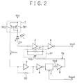
- Fig. 2 is a circuit diagram showing a first embodiment of the automatic gain switching-type burst optical signal receiving circuit of the present invention.
- the first embodiment of the automatic gain switching type burst optical signal receiving circuit of the present invention consists of a photodiode 1, a current mirror circuit 2, a first transimpedance amplifier 3, a first inverting amplifier 4, a second transimpedance amplifier 5, a second inverting amplifier 6, a peak-value detecting circuit 7, an operational amplifier 8, a feedback resistor unit Rf and a feedback resistor R2.
- the photodiode 1 receives an optical signal L and converts the received optical signal L to a receiving optical signal current Iin.
- the current mirror circuit 2 consists of PNP type transistors TR1 and TR2, and emitters of the PNP-type transistors TR1 and TR2 are connected, and a reverse bias voltage Vcc is applied to the emitters of the PNP-type transistors TR1 and TR2.
- the reverse bias voltage Vcc is also applied to a cathode of the photodiodel via the PNP-type transistor TR1. Bases of these PNP-type transistors TR1 and TR2 are connected to a collector of the PNP-type transistor TR1.
- a collector current Imon of the PNP-type transistor TR2 always becomes equal to a collector current of the PNP-type transistor TR1, that is, the receiving optical signal current Iin of the photodiode 1, and the receiving optical signal current Iin can be monitored by the collector current Imon of the PNP-type transistor TR2.
- the first transimpedance amplifier 3 converts the receiving optical signal current Iin obtained at the photodiode 1 to a voltage signal.
- the feedback resistor unit Rf connected in parallel with the first transimpedance amplifier 3 is provided between the input side and the output side of the first transimpedance amplifier 3.
- the feedback resistor unit Rf consists of a resistor R1 and a MOS transistor TR3, and the MOS transistor TR3 is connected in parallel with the resistor R1.
- the feedback resistor unit Rf is a feedback resistor that decides a gain of the first transimpedance amplifier 3.
- the resistance value of the feedback resistor unit Rf is decided by the parallel resistance value of the resistance value between source and drain of the MOS transistor TR3 and the resistor R1.
- the first inverting amplifier 4 inverts the output signal from the first transimpedance amplifier 3, and outputs the inverted signal as a voltage signal Vout to an external instrument.
- the second transimpedance amplifier 5 converts the collector current Imon of the PNP-type transistor TR2 to a voltage signal.
- the R2 is a feedback resistor deciding the gain of the second transimpedance amplifier 5, and the value of the TR2 is set as a smaller value than the R1.
- the second inverting amplifier 6 inverts and amplifies the output signal from the second transimpedance amplifier 5.
- the peak-value detecting circuit 7 detects a peak value Vpd of the outputted signal from the second inverting amplifier 6.
- a reset signal Reset is inputted to the peak-value detecting circuit 7 from the outside, and after every finish of inputting the burst signal, the peak value Vpd is made to reset.
- the operational amplifier 8 outputs a signal Vg in response to the level of the peak value Vpd to the gate of the MOS transistor TR3 and controls the gate voltage of the MOS transistor TR3.
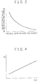
- Fig. 3 is a graph showing a characteristic of the MOS transistor TR3 in the feedback resistor unit Rf for the first transimpedance amplifier 3.
- the characteristic shows the relation a voltage between gate and source for an on resistance value between drain and source.
- a N-channel-type MOS transistor has a characteristic that the resistance value between drain and source becomes small when the voltage between gate and source is made to be large. Therefore, the resistance value between drain and source of the MOS transistor TR3 is controlled by controlling the voltage between gate and source of the MOS transistor TR3.
- the resistance value of the feedback resistor unit Rf is controlled and the conversion gain of the first transimpedance amplifier 3 is controlled.
- Fig. 4 is a graph showing an input/output characteristic of the operational amplifier 8. As shown in Fig. 4 for the operational amplifier 8, an output Vg for an input peak value Vpd has a linear characteristic. And the gradient and offset voltage are set beforehand so that the voltage between gate and source Vg becomes optimal for the peak value Vpd.
- FIG. 5 is a diagram showing waveforms of the first embodiment of the present invention. Referring to Fig. 5, the operation of the first embodiment of the present invention is explained. In Fig.
- the photodiodel receives the optical signal L and converts the received optical signal L to the receiving optical signal current Iin.
- the receiving optical signal current Iin is made to be the collector current of the PNP-type transistor TR1 being one of the TRs in the current mirror circuit 2.
- the monitor current Imon being the collector current of the TR2, which is equal to the receiving optical signal current Iin, appears.
- the monitor current Imon from the current mirror circuit 2 is inputted to the second transimpedance amplifier 5, and the second transimpedance amplifier 5 converts the monitor current Imon to a voltage signal.
- the output waveform " a " from the second transimpedance amplifier 5 becomes a waveform whose polarity is inverted to the monitor current Imon inputting to the second transimpedance amplifier 5.
- the gain of the second transimpedance amplifier 5, which is decided by the feedback resistor R2 is set to be a value that the output signal is not saturated even when a large signal is inputted. With this, the second transimpedance amplifier 5 amplifies linearly the amplitude of the monitor current Imon.
- the second inverting amplifier 6 inverts the output signal from the second transimpedance amplifier 5 and outputs a signal shown at the continuous line of the waveform " b ".
- the peak value detecting circuit 7 detects the peak value Vpd of the output signal from the second transimpedance amplifier 5 within one bit. As shown in the dotted line of the waveform " b ", the peak value detecting circuit 7 keeps the value during the burst interval decided by the reset signal Reset. In this, the reset signal Reset is shown in the waveform " c ". The kept peak value Vpd is initialized every burst cycle by the reset signal Reset shown in the waveform " c ".
- the output signal from the peak value detecting circuit 7 shown in the dotted line of waveform " b " is inputted to the operational amplifier 8.
- the operational amplifier 8 inverts the inputted signal and gives the voltage between gate and source Vg being the inverted signal to the gate of the MOS transistor TR3 in the feedback resistor unit Rf.
- This peak value Vpd shows the size of the monitor current Imon, that is, the receiving optical signal current Iin, therefore, the larger the receiving optical signal current Iin (the inputting level of the received optical signal L), the smaller the value of the feedback resistor unit Rf becomes, on the contrary, the smaller the receiving optical signal current Iin, the larger the value of the feedback resistor unit Rf becomes. And when the reset signal Reset is inputted, the value of the feedback resistor unit Rf is made to initialize to be the maximum value.
- the polarity of the output waveform " e " of the first transimpedance amplifier 3 is inverted to the receiving optical signal current Iin inputting to the transimpedance amplifier 3, this is similar to the output waveform " a " of the second transimpedance amplifier 5.
- the first transimpedance amplifier 3 receives this optical signal at a state that the first transimpedance amplifier 3 is in the maximum gain, as a result, the first bit signal reaches to the saturation state; however, this large optical signal is reflected to the monitor current Imon and the feedback resistor unit Rf is controlled to a small value at once.
- the first inverting amplifier 4 inverts the output signal from the first transimpedance amplifier 3, and outputs a signal Vout shown in the waveform " f ".
- the pulse width of the first bit is wide,caused by the saturation; however, a normal waveform can be obtained on and after the second bit.
- the gain of the first transimpedance amplifier 3, to which the receiving optical signal current is inputted, is switched in response to the power level of the receiving optical signal. Therefore, even when the power level of the optical signal L becomes large, a series of signals having low distortion can be obtained. And on the contrary, even when the power level of the optical signal L becomes small, a series of signals having required amplitude can be obtained.
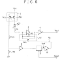
- Fig. 6 is a circuit diagram showing the second embodiment of the automatic gain switching type burst optical signal receiving circuit of the present invention.
- the circuit structure for main signal composed of the photodiodel, the current mirror circuit 2, the first transimpedance amplifier 3 and the first inverting amplifier 4 is the same as the structure of the first embodiment shown in Fig. 2.
- the second embodiment of the present invention shown in Fig. 6 is different from the first embodiment shown in Fig. 2 in an amplifying means for the monitor current Imon.
- the amplifying means for the monitor current Imon provides the second transimpedance amplifier 5, the feedback resistor R2 and the second inverting amplifier 6.
- the amplifying means for the monitor current Imon provides a resistor R3 whose one end is connected to the collector of the PNP-type transistor TR2 in the current mirror circuit 2 and whose other end is grounded, and a non-inverting amplifier 9 whose one end is connected to the one end of the resistor R3 and whose other end is connected to the peak-value detecting circuit 7. And a voltage signal generated at the resistor R3 is directly monitored in the second embodiment.
- the voltage signal generated at the resistor R3 is inputted to the peak-value detecting circuit 7 via the non-inverting amplifier 9.
- the peak-value detecting circuit 7 detects and keeps the peak value Vpd as the same as the first embodiment, and the resistance value of the feedback resistor unit Rf is controlled in response to this peak value Vpd.
- the circuit structure can be simplified. Especially in the case where strict accuracy for the gain control is not needed, this circuit structure is effective.
- the gain of the amplifier can be switched instantly (within one bit) in response to the inputting power level.
- the reason is that the input current is directly monitored and the gain is switched by the control of feedforward gain control structure, as a result, the oscillation caused by the high-speed response is not considered.
- the receiving dynamic range can be expanded easily. The reason is that even when a very large power level signal is inputted, the gain of the first stage amplifier is controlled to decrease, and the waveform distortion caused by the saturation can be prevented. Especially, at a DC-coupling-type circuit used frequently at the burst optical signal receiving circuit, when an optical signal having input offset is inputted, the waveform distortion caused by the saturation is liable to occur; therefore,this effect is usable.
- the current mirror circuit is used to generate the monitor current equal to the receiving optical signal current, and the feedback resistor is controlled.
- this is not limited to the current mirror circuit; for example, a photodiode for monitoring having an equal characteristic to the photodiode 1 can be provided, and a receiving optical signal current obtained by this photodiode for monitoring can be monitored and a feedback resistor can be controlled.
- the resistor R1 and the MOS transistor TR3 for feedback are connected in parallel; however, the resistor R1 can be used as an auxiliary function working in the case that the MOS transistor is cutoff. And as the MOS transistor, for example, a depletion-type can be used, and the resistor R1 can be eliminated.
- an optical signal is received and the received optical signal is converted to a current signal, and the current signal is converted to a voltage signal, and the current signal is monitored, and a conversion gain of a current-to-voltage converting means is controlled based on the monitored current signal so that the voltage signal is not saturated. Therefore, the gain of the current-to-voltage converting means (transimpedance amplifier) can be switched instantly in response to the power level of a burst optical signal, and even when an optical signal having large power level is inputted, an automatic gain switching-type burst optical signal receiving circuit, in which the waveform distortion is suppressed effectively, can be obtained.
- An automatic gain switching-type burst optical signal receiving circuit in which, even when an optical signal having a large power level is inputted, waveform distortion can be suppressed effectively.
- An optical-signal-to-current converting means composed of a photodiode, receives an optical signal and converts the received optical signal to a current signal Iin.
- a current-to-voltage converting means which is composed of a first transimpedance amplifier, a feedback resistor unit and a first inverting amplifier, converts the current signal Iin to a voltage signal.
- a current monitoring means composed of a current mirror circuit, generates a monitor current Imon by monitoring a current signal converted at the optical-signal-to-current converting means.
- a gain controlling means composed of a second transimpedance amplifier, a feedback resistor, a second inverting amplifier, a peak-value detecting circuit and an operational amplifier, controls a conversion gain of said current-to-voltage converting means based on said monitor current Imon monitored at said current monitoring means so that the voltage signal outputted from said current-to-voltage converting means is not saturated.
Landscapes
- Physics & Mathematics (AREA)
- Electromagnetism (AREA)
- Engineering & Computer Science (AREA)
- Computer Networks & Wireless Communication (AREA)
- Signal Processing (AREA)
- Optical Communication System (AREA)
- Amplifiers (AREA)
- Control Of Amplification And Gain Control (AREA)
Applications Claiming Priority (2)
| Application Number | Priority Date | Filing Date | Title |
|---|---|---|---|
| JP05198499A JP3329302B2 (ja) | 1999-02-26 | 1999-02-26 | 自動利得切換型バースト光受信回路 |
| JP5198499 | 1999-02-26 |
Publications (2)
| Publication Number | Publication Date |
|---|---|
| EP1032145A2 true EP1032145A2 (fr) | 2000-08-30 |
| EP1032145A3 EP1032145A3 (fr) | 2002-04-10 |
Family
ID=12902136
Family Applications (1)
| Application Number | Title | Priority Date | Filing Date |
|---|---|---|---|
| EP00301519A Withdrawn EP1032145A3 (fr) | 1999-02-26 | 2000-02-25 | Circuit récépteur optique de signaux à rafales à gain automatique de type à commutation |
Country Status (3)
| Country | Link |
|---|---|
| EP (1) | EP1032145A3 (fr) |
| JP (1) | JP3329302B2 (fr) |
| AU (1) | AU1943300A (fr) |
Cited By (8)
| Publication number | Priority date | Publication date | Assignee | Title |
|---|---|---|---|---|
| EP2391003A1 (fr) * | 2010-05-24 | 2011-11-30 | University College Cork | Récepteur de mode rafale linéaire |
| US8847140B2 (en) | 2012-03-07 | 2014-09-30 | Kabushiki Kaisha Toshiba | Light receiving circuit having an automatic threshold control circuit for forming and allowing electric current flowing between a second potential line and first and second connection points |
| US9712254B2 (en) | 2013-08-07 | 2017-07-18 | Mitsubishi Electric Corporation | Current-voltage conversion circuit, optical receiver, and optical terminator |
| CN108199696A (zh) * | 2018-03-06 | 2018-06-22 | 厦门优迅高速芯片有限公司 | 一种跨阻放大器自动增益控制电路 |
| US10079584B1 (en) | 2017-03-14 | 2018-09-18 | Futurewei Technologies, Inc. | Closed-loop automatic gain control in linear burst-mode transimpedance amplifier |
| CN111600659A (zh) * | 2020-04-30 | 2020-08-28 | 珠海格力电器股份有限公司 | 一种光接收电路 |
| CN113514152A (zh) * | 2021-06-18 | 2021-10-19 | 中国人民解放军国防科技大学 | 一种可鉴别信号来向的微弱光信号检测系统 |
| CN115473501A (zh) * | 2022-11-15 | 2022-12-13 | 上海阿米芯光半导体有限责任公司 | 跨阻放大器的调控电路及降低杂散电感对电路影响的方法 |
Families Citing this family (9)
| Publication number | Priority date | Publication date | Assignee | Title |
|---|---|---|---|---|
| JP3893969B2 (ja) | 2001-12-28 | 2007-03-14 | 日本電気株式会社 | 光受信装置 |
| KR100630083B1 (ko) * | 2002-04-26 | 2006-09-27 | 삼성전자주식회사 | 버스트모드 광 수신기의 자동이득조절 장치 |
| US7366428B2 (en) | 2003-09-16 | 2008-04-29 | Sumitomo Electric Indutries, Ltd. | Optical receiver |
| JP4821421B2 (ja) * | 2006-04-28 | 2011-11-24 | 住友電気工業株式会社 | 光受信器 |
| JP4892287B2 (ja) * | 2006-06-30 | 2012-03-07 | 富士通株式会社 | Pon通信用光パワーモニタ |
| JP4921510B2 (ja) * | 2009-04-09 | 2012-04-25 | Nttエレクトロニクス株式会社 | バースト光受信装置 |
| CN104685786A (zh) | 2012-09-27 | 2015-06-03 | 三菱电机株式会社 | 接收器以及接收方法 |
| JP6882861B2 (ja) * | 2016-07-14 | 2021-06-02 | キヤノン株式会社 | 半導体装置、液体吐出ヘッド、液体吐出ヘッドカートリッジおよび記録装置 |
| KR102466313B1 (ko) * | 2020-07-28 | 2022-11-10 | 이화여자대학교 산학협력단 | 자동 이득 조절 트랜스 임피던스 증폭기 |
Family Cites Families (3)
| Publication number | Priority date | Publication date | Assignee | Title |
|---|---|---|---|---|
| GB2293931B (en) * | 1994-10-07 | 1999-03-17 | Northern Telecom Ltd | Threshold setting device |
| US5532471A (en) * | 1994-12-21 | 1996-07-02 | At&T Corp. | Optical transimpedance amplifier with high dynamic range |
| US5565672A (en) * | 1994-12-30 | 1996-10-15 | Lucent Technologies Inc. | Optical transimpedance receiver with compensation network |
-
1999
- 1999-02-26 JP JP05198499A patent/JP3329302B2/ja not_active Expired - Fee Related
-
2000
- 2000-02-23 AU AU19433/00A patent/AU1943300A/en not_active Abandoned
- 2000-02-25 EP EP00301519A patent/EP1032145A3/fr not_active Withdrawn
Cited By (12)
| Publication number | Priority date | Publication date | Assignee | Title |
|---|---|---|---|---|
| EP2391003A1 (fr) * | 2010-05-24 | 2011-11-30 | University College Cork | Récepteur de mode rafale linéaire |
| WO2011147807A1 (fr) | 2010-05-24 | 2011-12-01 | University College Cork - National University Of Ireland, Cork | Récepteur linéaire à fonctionnement par salve |
| US20130121707A1 (en) * | 2010-05-24 | 2013-05-16 | Peter Ossieur | Linear burst mode receiver |
| US9059807B2 (en) * | 2010-05-24 | 2015-06-16 | University College Cork—National University of Ireland | Linear burst mode receiver |
| US8847140B2 (en) | 2012-03-07 | 2014-09-30 | Kabushiki Kaisha Toshiba | Light receiving circuit having an automatic threshold control circuit for forming and allowing electric current flowing between a second potential line and first and second connection points |
| US9712254B2 (en) | 2013-08-07 | 2017-07-18 | Mitsubishi Electric Corporation | Current-voltage conversion circuit, optical receiver, and optical terminator |
| US10079584B1 (en) | 2017-03-14 | 2018-09-18 | Futurewei Technologies, Inc. | Closed-loop automatic gain control in linear burst-mode transimpedance amplifier |
| CN108199696A (zh) * | 2018-03-06 | 2018-06-22 | 厦门优迅高速芯片有限公司 | 一种跨阻放大器自动增益控制电路 |
| CN108199696B (zh) * | 2018-03-06 | 2023-08-15 | 厦门优迅高速芯片有限公司 | 一种跨阻放大器自动增益控制电路 |
| CN111600659A (zh) * | 2020-04-30 | 2020-08-28 | 珠海格力电器股份有限公司 | 一种光接收电路 |
| CN113514152A (zh) * | 2021-06-18 | 2021-10-19 | 中国人民解放军国防科技大学 | 一种可鉴别信号来向的微弱光信号检测系统 |
| CN115473501A (zh) * | 2022-11-15 | 2022-12-13 | 上海阿米芯光半导体有限责任公司 | 跨阻放大器的调控电路及降低杂散电感对电路影响的方法 |
Also Published As
| Publication number | Publication date |
|---|---|
| JP3329302B2 (ja) | 2002-09-30 |
| JP2000252775A (ja) | 2000-09-14 |
| EP1032145A3 (fr) | 2002-04-10 |
| AU1943300A (en) | 2000-08-31 |
Similar Documents
| Publication | Publication Date | Title |
|---|---|---|
| EP1032145A2 (fr) | Circuit récépteur optique de signaux à rafales à gain automatique de type à commutation | |
| EP0568880B1 (fr) | Préamplificateur avec circuit de commande de gain pour communication optique | |
| JP3893969B2 (ja) | 光受信装置 | |
| JP3260263B2 (ja) | レーザー・ダイオード駆動装置 | |
| US5539779A (en) | Automatic offset control circuit for digital receiver | |
| KR100630083B1 (ko) | 버스트모드 광 수신기의 자동이득조절 장치 | |
| US6909082B2 (en) | Automatic threshold control device for burst mode optical receiver | |
| JPH04358443A (ja) | 光受信器 | |
| EP1746725B1 (fr) | Circuit amplificateur de signal | |
| US4393518A (en) | Optical communication arrangement | |
| US5517351A (en) | Optical receiver apparatus | |
| US20070104493A1 (en) | Optical receiver preamplifier | |
| JP3606143B2 (ja) | オフセット制御回路及びそれを用いた光受信器並びに光通信システム | |
| JP3058922B2 (ja) | 広ダイナミックレンジ光受信器 | |
| KR100547840B1 (ko) | 빠른 세틀링 시간을 갖는 자동 이득 제어 장치 | |
| US20020041417A1 (en) | Burst mode optical receiver using multi-stage feedback | |
| JPH11145913A (ja) | プリアンプ | |
| JPH0575544A (ja) | 自動利得調整回路 | |
| JP3230574B2 (ja) | 光受信回路 | |
| US5703504A (en) | Feedforward adaptive threshold processing method | |
| JP2002290168A (ja) | 光受信器 | |
| JP2600462B2 (ja) | 光受信回路 | |
| JPH0685556A (ja) | 増幅器 | |
| JP3612147B2 (ja) | 光受信回路及び光伝送システム | |
| JP2616680B2 (ja) | 光受信回路 |
Legal Events
| Date | Code | Title | Description |
|---|---|---|---|
| PUAI | Public reference made under article 153(3) epc to a published international application that has entered the european phase |
Free format text: ORIGINAL CODE: 0009012 |
|
| AK | Designated contracting states |
Kind code of ref document: A2 Designated state(s): AT BE CH CY DE DK ES FI FR GB GR IE IT LI LU MC NL PT SE Kind code of ref document: A2 Designated state(s): FR GB |
|
| AX | Request for extension of the european patent |
Free format text: AL;LT;LV;MK;RO;SI |
|
| PUAL | Search report despatched |
Free format text: ORIGINAL CODE: 0009013 |
|
| AK | Designated contracting states |
Kind code of ref document: A3 Designated state(s): AT BE CH CY DE DK ES FI FR GB GR IE IT LI LU MC NL PT SE |
|
| AX | Request for extension of the european patent |
Free format text: AL;LT;LV;MK;RO;SI |
|
| 17P | Request for examination filed |
Effective date: 20020327 |
|
| 17Q | First examination report despatched |
Effective date: 20021115 |
|
| AKX | Designation fees paid |
Free format text: FR GB |
|
| REG | Reference to a national code |
Ref country code: DE Ref legal event code: 8566 |
|
| STAA | Information on the status of an ep patent application or granted ep patent |
Free format text: STATUS: THE APPLICATION IS DEEMED TO BE WITHDRAWN |
|
| 18D | Application deemed to be withdrawn |
Effective date: 20030326 |