EP1034632B1 - Procede de transfert de signaux de donnees ainsi que procede et appareil de desynchronisation de signaux pdh - Google Patents
Procede de transfert de signaux de donnees ainsi que procede et appareil de desynchronisation de signaux pdh Download PDFInfo
- Publication number
- EP1034632B1 EP1034632B1 EP98956821A EP98956821A EP1034632B1 EP 1034632 B1 EP1034632 B1 EP 1034632B1 EP 98956821 A EP98956821 A EP 98956821A EP 98956821 A EP98956821 A EP 98956821A EP 1034632 B1 EP1034632 B1 EP 1034632B1
- Authority
- EP
- European Patent Office
- Prior art keywords
- frequency deviation
- clock signal
- pointer
- pdh
- signals
- Prior art date
- Legal status (The legal status is an assumption and is not a legal conclusion. Google has not performed a legal analysis and makes no representation as to the accuracy of the status listed.)
- Expired - Lifetime
Links
- 238000000034 method Methods 0.000 title claims description 14
- 238000009499 grossing Methods 0.000 description 18
- 230000001360 synchronised effect Effects 0.000 description 16
- 230000000694 effects Effects 0.000 description 8
- 230000001788 irregular Effects 0.000 description 5
- 238000001914 filtration Methods 0.000 description 3
- 230000005540 biological transmission Effects 0.000 description 2
- 230000003111 delayed effect Effects 0.000 description 1
- 230000008929 regeneration Effects 0.000 description 1
- 238000011069 regeneration method Methods 0.000 description 1
- 238000000926 separation method Methods 0.000 description 1
- 230000001960 triggered effect Effects 0.000 description 1
Images


Classifications
-
- H—ELECTRICITY
- H04—ELECTRIC COMMUNICATION TECHNIQUE
- H04J—MULTIPLEX COMMUNICATION
- H04J3/00—Time-division multiplex systems
- H04J3/02—Details
- H04J3/06—Synchronising arrangements
- H04J3/07—Synchronising arrangements using pulse stuffing for systems with different or fluctuating information rates or bit rates
- H04J3/076—Bit and byte stuffing, e.g. SDH/PDH desynchronisers, bit-leaking
Definitions
- the invention relates to a method of transferring data signals from a first PDH (Plesiochronous Digital Hierarchy) device via an SDH (Synchronous Digital Hierarchy) network to a second PDH device, wherein a clock signal is regenerated in the second PDH device on the basis of the data signals received, and wherein pointer adjustments may occur in the SDH network which are compensated in the second PDH device with a temporary frequency deviation in said regenerated clock signal.
- the invention moreover relates to a method and an apparatus for desynchronizing PDH signals which have been transferred via an SDH network in which pointer adjustments may occur, said pointer adjustments being compensated in the desynchronization with a temporary frequency deviation in a clock signal regenerated on the basis of the received PDH signals.
- An SDH network is frequently used for transferring data signals from one PDH device to another.
- all network elements in a synchronous state will be synchronized to a common reference clock signal, whereas the embedded PDH signals cannot be expected to be synchronous with the SDH network.
- this takes place by means of an associated PDH clock signal, and the signals are then transmitted in the network as pure SDH signals.
- Unpacking of the PDH signals takes place in the receiving network element, and in connection with this the associated PDH clock signal is regenerated. After suitable low-pass filtering, the regenerated PDH clock signal will substantially correspond to the original clock signal in the network element in which the signals were embedded; but small variations may occur, e.g. in the form of phase variations between the original PDH clock signal and the regenerated PDH clock signal.
- a more accurate clock signal is required at the receiver side, capable of ensuring that the receiver device may be synchronized to the device at the transmitter side, and a special reference clock signal therefore has to be transferred.
- a reference clock signal has previously been transferred via a separate network to ensure the quality. If, on the other hand, the reference clock signal is transferred via the SDH network, as described above, a sufficiently good quality of the signal cannot be obtained at the receiver side. The reason is primarily that pointer adjustments may occur in the SDH network.
- SDH networks are based on one or more stable clock signals. In spite of the fact that very stable references are present in the network, differences between phase and frequency of the references may occur.
- the network elements in such a communications network must be capable of tolerating these variations in phase and frequency, without data in the form of communications signals being lost. This may be ensured by performing pointer adjustments where a number of bits or bytes may be added or removed in the data flow.
- phase deviations between various points in the network may occur because of e.g. temperature impacts on the communications channels between the nodes of the network. These deviations take place very slowly, e.g. with a period of a day, and a relatively long time will therefore elapse between the pointer adjustments triggered because of these deviations.
- EP 535 698 describes a desynchronizer that can accommodate up to six consecutive pointer adjustments by means of an elastic store.
- EP 549 125 describes a desynchronizer having an improved jitter performance resulting from the use of a dynamic bit leaking arrangement.
- US 4 996 698 describes a way of smoothing the regenerated clock signal so that jitter is kept below certain limits.
- the smoothing of the effect of each pointer adjustment must take place relatively rapidly, thereby ensuring that the effect of one pointer adjustment has been smoothed before the next pointer adjustment occurs.
- the relatively rapid smoothing means that the stabilized clock signal will still include a certain residual jitter, which makes it impossible to maintain the synchronization in the following PDH synchronization device, since some applications, as mentioned above, require that a reference clock signal can be regenerated with great accuracy.
- a GSM base station e.g., requires an accuracy of the reference clock signal of ⁇ 0.050 ppm, corresponding to ⁇ 50 nsec per second.
- a known method trying to solve this problem comprises replacing the PDH reference clock signal in the SDH network element, which unpacks the PDH signal, by the synchronous clock signal from the SDH network element concerned in a so-called retiming circuit. While this may provide a reference clock signal without residual jitter, it requires that the PDH signals are synchronized to the SDH clock signal in the network element in which they are embedded in the SDH system, and, normally, this condition cannot be expected to be satisfied, or, at any rate, it puts severe limits to the application.
- the retiming circuit must comprise a frame buffer and be capable of introducing frame slips.
- the frame buffer causes the transferred signals to be delayed by 125 ⁇ sec corresponding to a frame, and the frame slip may cause certain signals, such as e.g. CRC4 signals, to be lost in the PDH synchronization unit.
- pointer adjustments from the SDH network accumulate in the buffer of the retiming circuit as the circuit maintains a constant data rate into the PDH device.
- the buffer may thus overflow, so that data losses may occur in connection with the frame slip.
- an object of the invention is to provide a method of the type mentioned in the opening paragraph in which jitter in the regenerated clock signal, at least when the SDH network is in a synchronous state, may be reduced to a level at which the synchronization in the subsequent PDH synchronization device may be maintained.
- a first pointer adjustment is compensated with a first, relatively low frequency deviation, and that, if one or more additional pointer adjustments occur before the compensation of the first pointer adjustment has been completed, compensation is subsequently performed with a second, relatively high frequency deviation.
- the regenerated clock signal may be produced by means of an analog phase-locked loop, as defined in claim 2, or by means of a digital phase-locked loop, as defined in claim 3.
- the relatively low frequency deviation is produced by limiting the said control signal to a given limit value, while the relatively high frequency deviation is produced by allowing the control signal to exceed said given limit value.
- the digital phase-locked loop in which a control word, which is capable of assuming one of a plurality of predetermined discrete values in response to a phase difference between the regenerated clock signal and a reference signal derived from the received data, is fed to a numerically controlled oscillator, and in which the control word assumes a nominal value when said phase difference is numerically smaller than a predetermined value, and assumes one of the other values when the phase difference is numerically greater than the predetermined value, the relatively high frequency deviation is produced in that said control word assumes one of the other values continuously, while the relatively low frequency deviation is produced by modulating the control word so that it assumes one of the other values in subperiods, while it assumes the nominal value in intermediate periods.
- the relatively low frequency deviation is less than ⁇ 0.050 ppm, it being then possible to satisfy the accuracy requirements of the reference clock signal that apply to e.g. GSM base stations.
- the relatively high frequency deviation is higher than ⁇ 4.6 ppm, as stated in claim 5, it is ensured that it is possible to compensate the pointer adjustments which occur when the SDH network is not in a synchronous state, since, according to the SDH specifications, these may maximally occur at such a rate as allows them to be compensated with this frequency deviation.
- the invention also relates to a corresponding method of desynchronizing PDH signals which have been transferred via an SDH network.
- a first pointer adjustment is compensated with a first relatively low frequency deviation, and, if one or more additional pointer adjustments occur before the compensation of the first pointer adjustment has been completed, compensation is subsequently performed with a second, relatively high frequency deviation, advantages corresponding to those mentioned above are obtained.
- the invention moreover relates to an apparatus for desynchronizing PDH signals which have been transferred via an SDH network.
- the apparatus When the apparatus is adapted to compensate a first pointer adjustment with a first, relatively low frequency deviation, and, if one or more additional pointer adjustments occur before the compensation of the first pointer adjustment has been completed, subsequently to compensate with a second, relatively high frequency deviation, the advantages described above are likewise obtained.
- the apparatus may comprise an analog phase-locked loop, as defined in claim 8, or a digital phase-locked loop, as defined in claim 9, for producing the regenerated clock signal.
- the analog phase-locked loop is adapted to feed a control signal, which is indicative of a phase difference between the regenerated clock signal and the received data, to a voltage-controlled oscillator, and to produce the relatively low frequency deviation by limiting said control signal to a given limit value and to produce the relatively high frequency deviation by allowing the control signal to exceed said given limit value.
- the digital phase-locked loop is adapted to feed a control word, which is capable of assuming one of a plurality of predetermined discrete values in response to a phase difference between the regenerated clock signal and a reference signal derived from the received data, to a numerically controlled oscillator, said control word being capable of assuming a nominal value when said phase difference is numerically smaller than a predetermined value, and of assuming one of the other values when the phase difference is numerically greater than the predetermined value.
- the apparatus is adapted to produce the relatively high frequency deviation by allowing said control word to assume one of the other values continuously, and to produce the relatively low frequency deviation by modulating the control word, so that it assumes one of the other values in subperiods, while it assumes the nominal value in intermediate periods.
- the relatively low frequency deviation is less than ⁇ 0.050 ppm, it being then possible to satisfy the accuracy requirements of the reference clock signal that apply to e.g. GSM base stations.
- the relatively high frequency deviation is higher than ⁇ 4.6 ppm, as defined in claim 11, it is ensured that it is possible to compensate the pointer adjustments which occur when the SDH network is not in a synchronous state, since, according to the SDH specifications, these may maximally occur at such a rate as allows them to be compensated with this frequency deviation.
- Fig. 1 shows an example of a network in which the invention may be applied.
- An SDH network 1 consists of a plurality of network elements, of which two network elements 2, 3 are shown in the figure.
- the network element 2 which may e.g. be a multiplexer
- signals from a PDH device 4 are loaded into the SDH network 1 to be carried via this to a second network element 3, where the signals are taken out again for a second PDH device 5.
- the network element 3 may e.g. be an Add and Drop Multiplexer (ADM) or a Digital Cross Connect (DXC).
- the transmission may e.g. take place as an STM-1 frame in the SDH network.
- the PDH signals, which, in the network element 2, are loaded into the SDH network may e.g. have a data rate of 2 Mbit/s, and they may be used inter alia for transferring a reference clock signal to a GSM base station, which will then be connected to the PDH device 5.
- the PDH signals of 2 Mbit/s from the STM-1 frame are unpacked in the PDH device 5.
- the PDH device 5 includes a synchronization circuit 6, which first generates a clock signal on the basis of the unpacked data signals, said clock signal containing gaps inter alia because of pointer adjustments performed in the SDH network, and then smoothes these gaps so as to create a stable clock signal of 2 MHz.
- This clock signal will correspond to the reference clock signal which, in the network element 2, was loaded into the SDH network, and it may e.g. be fed to the mentioned GSM base station.
- the synchronization circuit 6 will typically comprise a buffer and a phase-locked loop.
- Fig. 2 shows an embodiment of such a circuit using a traditional analog phase-locked loop.
- the circuit receives the data signals, which may e.g. be so-called TU-12 signals, from the network element 3.
- the TU-12 signals are unpacked to VC-12 signals in a demapping circuit 7, with simultaneous separation of overhead signals from the data signals proper.
- a clock signal is generated in the circuit 7 on the basis of the incoming data, a clock pulse being generated in principle for each data byte in the unpacked VC-12 signals.
- the circuit 7 may therefore add or remove clock pulses in the generated clock signal, which thereby becomes irregular, as the clock frequency will vary in step with the addition or removal of clock pulses. This frequency variation is called jitter.
- the unpacked VC-12 signals are input via a data bus in a buffer 8 by means of the clock signal which is generated in the circuit 7 and is possibly vitiated by jitter, so that the input will take place at an irregular rate depending on pointer adjustments, if any.
- the data buffer 8 may be constructed as a ring buffer and may e.g. be of 12 bytes.
- phase-locked loop which, as shown in fig. 2, may consist of a phase detector 9, a filter 10, a limiter circuit 11 and a voltage-controlled oscillator 12.
- the phase detector 9, the filter 10 and the voltage-controlled oscillator 12 are well-known in a phase-locked loop, while the limiter circuit 11 will be described more fully below.
- a new clock signal will appear on the output of the voltage-controlled oscillator 12, said new clock signal having an approximately constant frequency which corresponds to the mean frequency of the jitter clock signal.
- the phase detector 9 measures the phase difference between the jitter clock signal and the smoothed clock signal, and then a control signal, which controls the voltage-controlled oscillator 12, is generated via the filter 10 and the limiter circuit 11.
- the smoothed clock signal will typically have a frequency of 264 kHz; but since, normally, the signals are subsequently to be processed bitwise, the output signal from the voltage-controlled oscillator 12 will have a frequency eight times as high, viz. 2.112 MHz, which will then merely be divided by a factor of 8 before being used for the output of data from the buffer 8.
- the clock signal of 2.112 MHz is normally just called a 2 MHz signal and is therefore designated as such in the figure.
- the data signals may then be processed further, e.g. in the subsequent PDH device 5.
- the data signals of 2 Mbit/s, which are output from the buffer may contain the previously mentioned reference clock signal for e.g. a GSM base station.
- the two input signals to the phase detector 9 will substantially be uniform. Therefore, substantially no variations will take place in the output signal of the phase detector and thereby not in the control signal to the voltage-controlled oscillator 12 either.
- the limiter circuit 11, which is adapted to limit the fluctuations that may occur in the control signal to the voltage-controlled oscillator, will thus have no influence in this situation.
- the limiter circuit 11 is controlled by a detector circuit 13 which consists of a comparator 14 and a latch circuit 15.
- the comparator 14 is adapted to emit logical "1" to one input of the latch circuit 15 when the output signal from the phase detector 9 exceeds a fixed value REF, which will just be the case while a pointer adjustment is being smoothed.
- the other input of the latch circuit 15 is connected to the demapping circuit 7 and is logical "1" for a short period each time a pointer adjustment occurs.
- the demapping circuit 7 emits this short signal before it adds or removes a clock pulse in the generated clock signal.
- the latch circuit 15 is adapted to emit logical "0" when a pointer adjustment occurs, while a logical “1” from the comparator tells that the phase-locked loop is already in the process of smoothing a pointer adjustment.
- the latch circuit 15 emits logical "1” in all other situations.
- Logical “1” causes the limiter circuit 11 to limit the fluctuations in the control signal to the oscillator 12 and thereby its frequency change, while logical "0" puts no limitations on the control signal so that the frequency of the oscillator may vary freely.
- the detector circuit 13 will thus cause the limiter circuit 11 to limit the control signal to the voltage-controlled oscillator 12 to a predetermined value; but since, as mentioned, substantially no variations in this control signal occur, the limitation will be without importance.
- the demapping circuit 7 will emit a short signal to the other input of the latch circuit 15; but since the phase detector 9 does not yet detect a phase difference, the detector circuit 13 will thus still cause the limiter circuit 11 to limit the control signal to the voltage-controlled oscillator 12 to the predetermined value.
- the phase detector 9 detects a phase difference because of the removed or added clock pulse and therefore emits a control signal to the voltage-controlled oscillator 12 telling it to change frequency. Because of the limiter circuit 11, the variation of the control signal is limited, however, and the frequency variation will therefore also be limited to a value which is acceptable to the subsequent PDH device.
- the smoothing will of course take a correspondingly longer time because of the limited frequency variation. As the smoothing proceeds, the phase difference between the jitter clock signal and the smoothed clock signal diminishes, and the oscillator 12 will revert to the original frequency.
- the latch circuit 15 will emit logical "0", and the limiter circuit 11 will therefore no longer put limitations on the control signal to the oscillator 12.
- the full control signal from the phase detector 9 and the filter 10 can therefore now be fed to the oscillator, which will now smooth the phase difference with a considerably greater frequency change.
- the smoothing can hereby take place sufficiently rapidly for it to be completed before the next pointer adjustment occurs, as these can now be expected to occur at short intervals, e.g. because of missing synchronization somewhere in the SDH network.
- a single pointer adjustment caused e.g. by temperature impacts on the communications channels in the SDH network, may be compensated with a small frequency deviation, ensuring that a reference clock signal can still be passed on to the subsequent PDH device with sufficient accuracy. If, however, pointer adjustments occur at so short intervals that they cannot be compensated with the low frequency variation, this is caused by the fact that the SDH network is no longer in a synchronous state, and in that case it will not be possible to maintain the synchronization for the sensitive PDH device anyhow. Therefore, in this situation, compensation may be performed with a higher frequency deviation without further problems, thereby avoiding buffer overflow.
- Fig. 3 shows an alternative embodiment of a synchronization circuit in which a digital phase-locked loop is used instead of a traditional analog phase-locked loop, as described above.
- the mode of operation of the demapping circuit 7 and the buffer 8 is the same as for the embodiment of fig. 2, and here too smoothing of the irregular rate is performed by passing the jitter clock signal through a phase-locked loop, which, as shown in the figure, may consist of a filter 13, a modulator 14 and a numerically controlled oscillator 15.
- a phase detector must be provided like in the case of the analog loop; but it is formed by the buffer 8 here, which, as mentioned above, may e.g. consist of 12 storage locations or bytes, each having the size of 8 bits and indexed with an address.
- the difference between the address to which input takes place and the address from which output takes place indicates the filling degree of the buffer.
- This value of the filling degree is indicative of the phase difference between the two clock signals, and instead of comparing these in a traditional phase detector, a signal from the buffer 8, which indicates its filling degree, may therefore be fed to the filter 13.
- the filter 13 On the basis of this signal, the filter 13 generates a control word which, if the modulator 14 is disregarded, controls the numerically controlled oscillator 15.
- the oscillator 15 may be implemented as a programmable divider which, depending on the control word, can divide a system clock signal having a higher frequency by a factor which is determined by the control word.
- the control word may e.g. assume the three values ⁇ -1, 0, +1 ⁇ . If a system clock signal of 19.44 MHz is used, the oscillator may be adapted to divide by a factor of 9.204545 corresponding to the desired frequency of 2.112 MHz when the control word is 0.
- the oscillator can divide by a factor of 9.204611 corresponding to a frequency of 2.111985 MHz.
- division may correspondingly take place by a factor of 9.204482 corresponding to a frequency of 2.112015 MHz.
- the oscillator can just emit these discrete frequencies in principle.
- the two frequencies of 2.111985 MHz and 2.112015 MHz, respectively, correspond to a deviation from the desired frequency of about 7 ppm, which is sufficient for smoothing the effect of pointer adjustments, which occur at short intervals because of missing synchronization in a part of the SDH network.
- the frequency deviation is much greater than the deviation of ⁇ 0.050 ppm in the reference clock signal that can be accepted by e.g. a GSM base station.
- the frequency of the numerically controlled oscillator must therefore be capable of being adjusted in considerably smaller jumps than is possible with the frequencies mentioned above.
- the modulator 14 is inserting the modulator 14 between the filter 13 and the oscillator 15. Instead of passing the control word of -1 or +1, emitted by the filter 13, directly to the oscillator 15, as described before, it is now passed to the modulator 14, in which it is modulated with a square-wave signal from a pulse generator 17.
- the pulse generator 17 is controlled from a processor 16.
- the square-wave signal has a fixed period of e.g. 256 msec, whereas the pulse width is variable in steps of e.g. 1 msec.
- the square-wave signal from the pulse generator 17 is applied to the modulation input of the modulator and thereby determines the emitted control word.
- control word -1 or +1 When the square-wave signal is high, the control word -1 or +1 is emitted, while the control word 0 is emitted in the gaps between the pulses. This means that the control word -1 or +1 will just be emitted for a fraction of the time, and the oscillator 15 will use the higher or the lower frequency also just for a fraction of the time, while it will continue to use the nominal frequency for the rest of the time.
- the oscillator will emit a frequency which differs considerably less from the nominal frequency than the previously mentioned difference between two adjacent frequencies.
- the frequency may here be selected in jumps of 1/256 of the difference between 2.111985 MHz and 2.112000 MHz, corresponding to a frequency deviation of about 0.028 ppm, which is less than the 0.050 ppm which can maximally be accepted by the sensitive PDH device.
- the pulse width of the square-wave signal emitted by the pulse generator 17 is controlled from a processor 16, as mentioned before. This decides on the basis of information from the demapping circuit 7 and the filter 13, respectively, whether or not the control word is to be modulated, and if so, then with which pulse width.
- the processor 16 will decide to modulate the control word so that the effect is smoothed with the small frequency deviation.
- the smoothing will of course take a correspondingly longer time because of the limited frequency variation.
- the buffer fill diminishes, which corresponds to the phase difference between the jitter clock signal and the smoothed clock signal, and the oscillator 15 will revert to the original frequency.
- the processor will stop modulating the control word, and the oscillator will now smooth the phase difference with the considerably greater frequency change.
- the smoothing can hereby take place sufficiently rapidly for it to be completed before the next pointer adjustment takes place, as these can now be expected to occur at short intervals, e.g. because of missing synchronization somewhere in the SDH network.
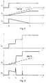
- Fig. 4 shows an example of the phase variations which may occur in the circuit shown in fig. 3 when a single pointer adjustment occurs in the SDH network.
- P i indicates the phase jump which occurs in the jitter clock signal when a pointer adjustment occurs at the time t a
- P o correspondingly shows the phase variation in the smoothed clock signal.
- P d shows the difference between the two signals P i and P o , which corresponds to the buffer fill.
- the curve for P d will not be a continuous curve in practice, but a stepped curve, as the buffer fill constitutes an integer number of bytes. It will be seen from the curves that the variation in the smoothed clock signal keeps below the limit given by MRTIE, and the data signals emitted from the buffer will thus satisfy the previously mentioned requirements.
- the effect of the pointer adjustment has been smoothed at the time t b , and the jitter clock signal and the smoothed clock signal are again in phase.
- Fig. 5 correspondingly shows the situation when several successive pointer adjustments occur at relatively short intervals, as will e.g. be the case when the SDH network is not in a synchronous state.
- the first pointer adjustment occurs at the time t a , and in the beginning the curves correspond completely to fig. 4.
- the next pointer adjustment occurs, and smoothing is now performed with the greater frequency deviation to avoid buffer overflow.
- the curve MRTIE is hereby exceeded; but this is accepted, since in this situation it will not be possible to maintain the synchronization of the sensitive PDH equipment anyhow.
- a pointer adjustment occurs again at the time t d . And it is smoothed in the figure by the greater frequency variation too. Since the previous adjustment is smoothed here, it may also be decided to have this smoothed with the small frequency deviation, since it is not known whether it might be the last one of a plurality of adjustments.
Landscapes
- Engineering & Computer Science (AREA)
- Computer Networks & Wireless Communication (AREA)
- Signal Processing (AREA)
- Synchronisation In Digital Transmission Systems (AREA)
- Stabilization Of Oscillater, Synchronisation, Frequency Synthesizers (AREA)
Claims (11)
- Procédé de transfert de signaux de données depuis un premier dispositif PDH (4) par le biais d'un réseau SDH (1) vers un second dispositif PDH (5), dans lequel un signal d'horloge est régénéré dans le second dispositif PDH (5) en fonction des signaux de données reçus, et dans lequel des ajustements de pointeur peuvent se produire dans le réseau SDH (1) et sont compensés dans le second dispositif PDH (5) par un écart de fréquence temporaire dans ledit signal d'horloge régénéré,
caractérisé en ce qu'un premier ajustement de pointeur est compensé par un premier écart basse fréquence, et en ce que, si un ou plusieurs ajustements de pointeur supplémentaires se produisent avant que la compensation du premier ajustement de pointeur soit terminée, la compensation est effectuée par la suite en utilisant un second écart haute fréquence. - Procédé selon la revendication 1, caractérisé en ce que le signal d'horloge régénéré est produit par le biais d'une boucle à verrouillage de phase analogique, un signal de commande variable indiquant une différence de phase entre le signal d'horloge régénéré et les données reçues étant envoyé vers un oscillateur commandé en tension (12) ;
et en ce que l'écart basse fréquence est produit en limitant l'écart dudit signal de commande à une valeur limite donnée, tandis que l'écart haute fréquence est produit en permettant à l'écart du signal de commande de dépasser ladite valeur donnée. - Procédé selon la revendication 1, caractérisé en ce que le signal d'horloge régénéré est produit par le biais d'une boucle à verrouillage de phase numérique, un mot de commande pouvant adopter une parmi plusieurs valeurs discrètes prédéterminées en réponse à une différence de phase entre le signal d'horloge régénéré et un signal de référence dérivé des données reçues étant envoyé vers un oscillateur commandé numériquement (15), lequel mot de commande adopte une valeur nominale lorsque ladite différence de phase est inférieure à une valeur prédéterminée et adopte une des autres valeurs lorsque la différence de phase est numériquement supérieure à la valeur prédéterminée ;
et en ce que l'écart haute fréquence est produit lorsque ledit mot de commande adopte une des autres valeurs continuellement, tandis que l'écart basse fréquence est produit en modulant le mot de commande de sorte qu'il adopte une des autres valeurs pendant des sous-périodes alors qu'il adopte la valeur nominale pendant des périodes intermédiaires. - Procédé selon les revendication 1 à 3, caractérisé en ce que l'écart basse fréquence est inférieur à ± 0,050 ppm.
- Procédé selon les revendication 1 à 4, caractérisé en ce que l'écart haute fréquence est supérieur à ± 4,6 ppm.
- Procédé de désynchronisation de signaux PDH qui ont été transférés par le biais d'un réseau SDH (1) dans lequel des ajustements de pointeur peuvent se produire, lesquels ajustements de pointeur sont compensés en désynchronisation par un écart de fréquence temporaire du signal d'horloge régénéré en fonction des signaux PDH reçus,
caractérisé en ce qu'un premier ajustement de pointeur est compensé par un premier écart basse fréquence, et en ce que, si un ou plusieurs ajustements de pointeur supplémentaires se produisent avant que la compensation du premier ajustement de pointeur soit terminée, la compensation est effectuée par la suite en utilisant un second écart haute fréquence. - Appareil de désynchronisation de signaux PDH qui ont été transférés par le biais d'un réseau SDH (1) dans lequel des ajustements de pointeur peuvent se produire, lesquels ajustements de pointeur sont compensés en désynchronisation par un écart de fréquence temporaire du signal d'horloge régénéré en fonction des signaux PDH reçus,
caractérisé en ce qu'il est conçu pour compenser un premier ajustement de pointeur par un premier écart basse fréquence, et, si un ou plusieurs ajustements de pointeur supplémentaires se produisent avant que la compensation du premier ajustement de pointeur soit terminée, pour effectuer une compensation par la suite en utilisant un second écart haute fréquence. - Appareil selon la revendication 7, caractérisé en ce qu'il comprend une boucle à verrouillage de phase analogique permettant de produire le signal d'horloge régénéré, laquelle boucle à verrouillage de phase est conçue pour envoyer un signal de commande variable indiquant une différence de phase entre le signal d'horloge régénéré et les données reçues vers un oscillateur commandé en tension (12) ;
et en ce qu'il est conçu pour produire un écart basse fréquence en limitant l'écart dudit signal de commande à une valeur limite donnée, et pour produire un écart haute fréquence en permettant à l'écart du signal de commande de dépasser ladite valeur donnée. - Appareil selon la revendication 7, caractérisé en ce qu'il comprend une boucle à verrouillage de phase numérique permettant de produire le signal d'horloge régénéré, laquelle boucle à verrouillage de phase est conçue pour envoyer un mot de commande pouvant adopter une parmi plusieurs valeurs discrètes prédéterminées, en réponse à une différence de phase entre le signal d'horloge régénéré et un signal de référence dérivé des données reçu, vers un oscillateur commandé numériquement (15), lequel mot de commande peut adopter une valeur nominale lorsque ladite différence de phase est numériquement inférieure à une valeur prédéterminée et peut adopter une des autres valeurs lorsque la différence de phase est numériquement supérieure à la valeur prédéterminée ;
et en ce qu'il est conçu pour produire l'écart haute fréquence en permettant au dit mot de commande d'adopter une des autres valeurs continuellement, et pour produire l'écart basse fréquence en modulant le mot de commande de sorte qu'il adopte une des autres valeurs pendant des sous-périodes alors qu'il adopte la valeur nominale pendant des périodes intermédiaires. - Appareil selon les revendications 7 à 9, caractérisé en ce que l'écart basse fréquence est inférieur à ± 0,050 ppm.
- Appareil selon les revendications 7 à 9, caractérisé en ce que l'écart haute fréquence est supérieur à ± 4,6 ppm.
Applications Claiming Priority (3)
| Application Number | Priority Date | Filing Date | Title |
|---|---|---|---|
| DK132697 | 1997-11-20 | ||
| DK132697A DK176259B1 (da) | 1997-11-20 | 1997-11-20 | Fremgangsmåde til overföring af datasignaler samt fremgangsmåde og apparat til desynkronisering af PDH-signaler |
| PCT/DK1998/000501 WO1999027669A1 (fr) | 1997-11-20 | 1998-11-19 | Procede de transfert de signaux de donnees ainsi que procede et appareil de desynchronisation de signaux pdh |
Publications (2)
| Publication Number | Publication Date |
|---|---|
| EP1034632A1 EP1034632A1 (fr) | 2000-09-13 |
| EP1034632B1 true EP1034632B1 (fr) | 2004-09-22 |
Family
ID=8103608
Family Applications (1)
| Application Number | Title | Priority Date | Filing Date |
|---|---|---|---|
| EP98956821A Expired - Lifetime EP1034632B1 (fr) | 1997-11-20 | 1998-11-19 | Procede de transfert de signaux de donnees ainsi que procede et appareil de desynchronisation de signaux pdh |
Country Status (5)
| Country | Link |
|---|---|
| EP (1) | EP1034632B1 (fr) |
| AU (1) | AU1333299A (fr) |
| DE (1) | DE69826516T2 (fr) |
| DK (1) | DK176259B1 (fr) |
| WO (1) | WO1999027669A1 (fr) |
Families Citing this family (2)
| Publication number | Priority date | Publication date | Assignee | Title |
|---|---|---|---|---|
| CN1848717B (zh) | 2005-04-15 | 2011-04-06 | 华为技术有限公司 | 获得异步解映射时钟的方法及电路 |
| CN101188468B (zh) * | 2006-11-17 | 2011-05-25 | 中兴通讯股份有限公司 | 同步数字体系中产生符合标准频偏的告警信号的装置 |
Family Cites Families (5)
| Publication number | Priority date | Publication date | Assignee | Title |
|---|---|---|---|---|
| US4996698A (en) * | 1989-10-23 | 1991-02-26 | Rockwell International Corporation | Clock signal resynchronizing apparatus |
| US5200982A (en) * | 1991-10-02 | 1993-04-06 | Alcatel Network Systems, Inc. | In-line piece-wise linear desynchronizer |
| US5268935A (en) * | 1991-12-20 | 1993-12-07 | At&T Bell Laboratories | Synchronous digital signal to asynchronous digital signal desynchronizer |
| FI94812C (fi) * | 1993-05-18 | 1995-10-25 | Nokia Telecommunications Oy | Menetelmä ja laite tasauspäätöksen aikaansaamiseksi synkronisen digitaalisen tietoliikennejärjestelmän solmupisteessä |
| JP2725692B2 (ja) * | 1995-05-12 | 1998-03-11 | 日本電気株式会社 | 140mクロック・stm−1電気クロック生成方式 |
-
1997
- 1997-11-20 DK DK132697A patent/DK176259B1/da not_active IP Right Cessation
-
1998
- 1998-11-19 AU AU13332/99A patent/AU1333299A/en not_active Abandoned
- 1998-11-19 WO PCT/DK1998/000501 patent/WO1999027669A1/fr not_active Ceased
- 1998-11-19 DE DE69826516T patent/DE69826516T2/de not_active Expired - Lifetime
- 1998-11-19 EP EP98956821A patent/EP1034632B1/fr not_active Expired - Lifetime
Also Published As
| Publication number | Publication date |
|---|---|
| EP1034632A1 (fr) | 2000-09-13 |
| DK176259B1 (da) | 2007-05-07 |
| WO1999027669A1 (fr) | 1999-06-03 |
| DE69826516T2 (de) | 2005-11-17 |
| DE69826516D1 (de) | 2004-10-28 |
| AU1333299A (en) | 1999-06-15 |
| DK132697A (da) | 1999-05-21 |
Similar Documents
| Publication | Publication Date | Title |
|---|---|---|
| US5343476A (en) | Transmission system for the synchronous digital hierarchy | |
| JP3866826B2 (ja) | デジタル電気通信伝送システム | |
| US6229863B1 (en) | Reducing waiting time jitter | |
| CA2062849C (fr) | Systeme de transmission pour la hierarchie numerique synchrone | |
| US5537447A (en) | Synchronous transmission system for carrying multiplexed signals | |
| EP0830760B1 (fr) | Desynchroniseur numerique | |
| JP3305320B2 (ja) | 同期解除装置 | |
| EP1965528B1 (fr) | Système de transmission optique et procédé | |
| US5796796A (en) | Pointer adjustment jitter cancellation processor utilizing phase hopping and phase leaking techniques | |
| EP0450269B1 (fr) | Dispositif de boucle à verrouillage de phase | |
| JP4560133B2 (ja) | 光インタフェース方法及びその装置 | |
| US20020186719A1 (en) | Pointer adjustment wander and jitter reduction apparatus for a desynchronizer | |
| CA2472691C (fr) | Traitement numerique des pointeurs sonet | |
| US7212599B2 (en) | Jitter and wander reduction apparatus | |
| EP1034632B1 (fr) | Procede de transfert de signaux de donnees ainsi que procede et appareil de desynchronisation de signaux pdh | |
| US5768328A (en) | Method and a receiver circuit for desynchronization in a digital transmission system | |
| EP1675291B1 (fr) | Filtre d'horloge digitale | |
| EP0947050B1 (fr) | Boucle numerique a phase asservie et son procede de commande, et procede et circuit de reception pour desynchronisation dans un systeme de transmission numerique | |
| EP0941589B1 (fr) | Procede et circuit pour produire un signal d'horloge de systeme | |
| US7440533B2 (en) | Modulated jitter attenuation filter | |
| JP4118175B2 (ja) | ジッタ抑制方法及び装置 | |
| CA2063930C (fr) | Desynchronisateur de conversion de signaux numeriques synchrones en signaux numeriques asynchrones | |
| EP0943193B1 (fr) | Procede et circuit pour produire un signal d'horloge central | |
| CA2316443A1 (fr) | Synchronisation par cartographie d'un signal module .delta.-. sigma. a sautillement de deplacement de frequences | |
| JPH03244237A (ja) | 非同期データ伝送システム |
Legal Events
| Date | Code | Title | Description |
|---|---|---|---|
| PUAI | Public reference made under article 153(3) epc to a published international application that has entered the european phase |
Free format text: ORIGINAL CODE: 0009012 |
|
| 17P | Request for examination filed |
Effective date: 20000619 |
|
| AK | Designated contracting states |
Kind code of ref document: A1 Designated state(s): DE FI FR GB IT |
|
| GRAP | Despatch of communication of intention to grant a patent |
Free format text: ORIGINAL CODE: EPIDOSNIGR1 |
|
| GRAS | Grant fee paid |
Free format text: ORIGINAL CODE: EPIDOSNIGR3 |
|
| GRAA | (expected) grant |
Free format text: ORIGINAL CODE: 0009210 |
|
| AK | Designated contracting states |
Kind code of ref document: B1 Designated state(s): DE FI FR GB IT |
|
| PG25 | Lapsed in a contracting state [announced via postgrant information from national office to epo] |
Ref country code: FI Free format text: LAPSE BECAUSE OF FAILURE TO SUBMIT A TRANSLATION OF THE DESCRIPTION OR TO PAY THE FEE WITHIN THE PRESCRIBED TIME-LIMIT Effective date: 20040922 |
|
| REG | Reference to a national code |
Ref country code: GB Ref legal event code: FG4D |
|
| REF | Corresponds to: |
Ref document number: 69826516 Country of ref document: DE Date of ref document: 20041028 Kind code of ref document: P |
|
| ET | Fr: translation filed | ||
| PLBE | No opposition filed within time limit |
Free format text: ORIGINAL CODE: 0009261 |
|
| STAA | Information on the status of an ep patent application or granted ep patent |
Free format text: STATUS: NO OPPOSITION FILED WITHIN TIME LIMIT |
|
| 26N | No opposition filed |
Effective date: 20050623 |
|
| PGFP | Annual fee paid to national office [announced via postgrant information from national office to epo] |
Ref country code: DE Payment date: 20091013 Year of fee payment: 12 |
|
| PGFP | Annual fee paid to national office [announced via postgrant information from national office to epo] |
Ref country code: IT Payment date: 20091118 Year of fee payment: 12 Ref country code: GB Payment date: 20091013 Year of fee payment: 12 Ref country code: FR Payment date: 20091125 Year of fee payment: 12 |
|
| GBPC | Gb: european patent ceased through non-payment of renewal fee |
Effective date: 20101119 |
|
| REG | Reference to a national code |
Ref country code: DE Ref legal event code: R119 Ref document number: 69826516 Country of ref document: DE Effective date: 20110601 Ref country code: DE Ref legal event code: R119 Ref document number: 69826516 Country of ref document: DE Effective date: 20110531 |
|
| REG | Reference to a national code |
Ref country code: FR Ref legal event code: ST Effective date: 20110801 |
|
| PG25 | Lapsed in a contracting state [announced via postgrant information from national office to epo] |
Ref country code: DE Free format text: LAPSE BECAUSE OF NON-PAYMENT OF DUE FEES Effective date: 20110531 |
|
| PG25 | Lapsed in a contracting state [announced via postgrant information from national office to epo] |
Ref country code: FR Free format text: LAPSE BECAUSE OF NON-PAYMENT OF DUE FEES Effective date: 20101130 |
|
| PG25 | Lapsed in a contracting state [announced via postgrant information from national office to epo] |
Ref country code: GB Free format text: LAPSE BECAUSE OF NON-PAYMENT OF DUE FEES Effective date: 20101119 |
|
| PG25 | Lapsed in a contracting state [announced via postgrant information from national office to epo] |
Ref country code: IT Free format text: LAPSE BECAUSE OF NON-PAYMENT OF DUE FEES Effective date: 20101119 |