EP1035551A2 - Résistance variable par rotation et système de contrôle l'utilisant - Google Patents
Résistance variable par rotation et système de contrôle l'utilisant Download PDFInfo
- Publication number
- EP1035551A2 EP1035551A2 EP00105001A EP00105001A EP1035551A2 EP 1035551 A2 EP1035551 A2 EP 1035551A2 EP 00105001 A EP00105001 A EP 00105001A EP 00105001 A EP00105001 A EP 00105001A EP 1035551 A2 EP1035551 A2 EP 1035551A2
- Authority
- EP
- European Patent Office
- Prior art keywords
- resistive film
- conductive member
- resistor
- brush
- unit
- Prior art date
- Legal status (The legal status is an assumption and is not a legal conclusion. Google has not performed a legal analysis and makes no representation as to the accuracy of the status listed.)
- Granted
Links
Images



Classifications
-
- H—ELECTRICITY
- H01—ELECTRIC ELEMENTS
- H01C—RESISTORS
- H01C10/00—Adjustable resistors
- H01C10/30—Adjustable resistors the contact sliding along resistive element
- H01C10/32—Adjustable resistors the contact sliding along resistive element the contact moving in an arcuate path
- H01C10/34—Adjustable resistors the contact sliding along resistive element the contact moving in an arcuate path the contact or the associated conducting structure riding on collector formed as a ring or portion thereof
Definitions
- the present invention relates to a rotary variable resistor which is operable by repeatedly rotating the operation shaft thereof and used for various electronic apparatuses, and, an output regulator using the same.
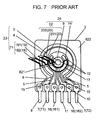
- a conventional rotary variable resistor which is operable by repeatedly rotating the operation shaft thereof is described hereinafter on reference to Fig. 6, Fig. 7 and Fig. 8.
- a resistor board 2 is fixed by insertion-molding.
- a round hole 821 is formed in such a manner as to be concentric with a round hole 811 formed at the center of the bottom of the case 1.
- Fig. 7 which is a schematic diagram showing the main portion of the conventional rotary variable resistor, the resistor board 2 is formed as follows.
- a horseshoe-shaped first resistive film 3 is formed on the upper surface of an insulating substrate 822.
- a horseshoe-shaped first current collecting member 4 formed with argentic material by printing is disposed in such a manner as to be concentric with the central round hole 821 and to face the opening thereof toward the same direction with the facing direction of the opening of the first resistive film 3.
- lead members 5 extend outward and are respectively connected to terminals 7 (71, 72) by caulking.
- a lead member 6 extends outward and is connected to a terminal 8 by caulking.
- annular second current collecting member 9 is formed by printing at the innermost position in such a manner as to be concentric with the round hole 821. From the second current collecting member 9, a lead member 10 extends outward and is connected to a terminal 11 by caulking.
- a pair of circular arc shaped conductive members 12 formed with argentic material by printing are disposed between the opening side portion of the first resistive film 3 and the second current collecting member 9 in such a manner as to be concentric with the round hole 821.
- insulating resist 13 is applied in such a manner as to cover a larger angular range than the angular opening of the first resistive film 3. In this case, the respective end portions (i.e., upper end portions in Fig.7) of the conductive members 12 are left without applying the resist 13.
- a horseshoe-shaped second resistive film 14 is formed by printing in such a manner as to cover a larger angular range than the angular opening of the first resistive film 3.
- the respective ends of the second resistive film 14 is electrically connected to the respective end portions (i.e., upper end portions in Fig. 7) of the conductive members 12, where the insulating resist 13 is not applied.
- lead members 15 extend outward and are respectively connected to terminals 16 (161, 162) by caulking.
- an operation shaft 17 made of insulating resin is disposed in such a manner as to protrude outward through the hole 181 of a bearing member 18 which is fixed to the case 1 with a metal cover 25.
- a round protrusion 171 formed at the center of the bottom of the operation shaft 17 engages with the respective round holes (811, 821) of the case 1 and the resistor board 2, whereby the shaft 17 is supported in such a manner as to be repeatedly rotatable.
- a first brush 21 and a second brush 22 respectively made of elastic metal plates are disposed in such a manner as to be electrically isolated each other.
- the contact portions 19 (191, 192) of the first brush 21 and the contact portions 20 (201, 202) of the second brush 22 are disposed in such a manner as to be on a straight line extended along the radius of the operation shaft 17 (the radius starts from the rotation axis of the operation shaft).
- the contact portion 191 of the first brush 21 elastically contacts to the first resistive film 3, and the contact portion 192 of the same elastically contacts to the first current collecting member 4.
- the first brushes 21, the first resistive film 3 and the first current collecting member 4 form a first resistor unit 23.
- the contact portion 201 of the second brush 22 elastically contacts to the second resistive film 14, and the contact portion 202 of the same elastically contacts to the second current collecting member 9.
- the second brush 22, the second resistive film 14 and the second current collecting member 9 form a second resistor unit 24.
- the contact portions 19 (191, 192) of the first brush 21 and the contact portions 20 (201, 202) of the second brush 22 slide on the respective printed patterns elastically contacting to these patterns, whereby output voltage at a predetermined rotational angle of the operation shaft 17 is obtained either from the first resistor unit 23 though the terminals 71 and 8 for instance, or from the second resistor unit 24 through the terminals 162 and 11 for instance.
- either of the effective output voltage is selected on the overlapping portions based on the judgment of a computer or the like, whereby effective output voltage is successively obtained either from the first resistor unit 23 or from the second resistor unit 24.
- the second resistive film 14 is formed on resist 13 applied on the predetermined portions of the conductive member 12 and the lead member 10 of the second current collecting member 9, also, for the input and the output to and from the first and the second resistor units (23, 24), six terminals (71, 72, 8, 11, 161 and 162) are needed. Therefore, the pattern structure is complicated, which requires many and complicated production processes.
- the object of the present invention is to address the above conventional problems and to provide a rotary variable resistor which is operable by repeatedly rotating the operation shaft thereof and has simple pattern structure on the resistor board thereof, also has a few terminals. It is a further object of the present invention to provide an output regulator which uses the above rotary variable resistor.
- the rotary variable resistor of the present invention comprises:
- the rotary variable resistor of the present invention having the above structure, one resistive film is commonly used for the first and the second resistor units, and the multilayer pattern as in the conventional structure is eliminated, whereby the pattern structure of the resistor board is simplified, also the number of terminals is decreased, accordingly the production process is simplified and the cost is also decreased.
- the output regulator of the present invention comprises:
- Fig. 1 is a schematic diagram showing the main portions of a rotary variable resistor in a first exemplary embodiment of the present invention
- Fig. 2 shows the characteristics of the output voltage of the rotary variable resistor in the same.
- the rotary variable resistor of this exemplary embodiment is different from the conventional rotary variable resistor in the pattern structure, the terminal structure and the elastically contacting positions of a first brush 31 and a second brush 32, which are respectively disposed on a resistor board 30.
- structure and functions are same with the conventional rotary variable resistor. Therefore the illustrations and the descriptions on these components are omitted.
- the resistor board 30 of this exemplary embodiment is formed as follows. That is, a horseshoe-shaped resistive film 33 is formed by printing on an insulating substrate 302 which has a round hole 301 at the center thereof. From the respective ends of the resistive film 33, lead members 34 made of argentic material extend outward and are respectively connected to terminals 35 (351, 352).
- an annular current collecting conductive member 36 formed with argentic material by printing is disposed in such a manner as to be concentric with the resistive film 33 and to be spatially isolated from the resistive film 33 and the lead members 34. From the current collecting conductive member 36, a lead member 37 extends outward and is connected to a terminal 38.
- a circular arc shaped auxiliary conductive member 39 formed with argentic material by printing is disposed in such a manner as to be concentric with the resistive film 33 and the current collecting conductive member 36, and, to be spatially isolated from the resistive film 33, the current collecting conductive member 36 and the lead members (34, 37), also to cover a larger angular range than the angular opening of the resistive film 33.
- a lead member 40 extends outward and is connected to a terminal 41.
- a first brush 31 and a second brush 32 which respectively elastically contact to the respective patterns formed on the resistor board 30, are fixed to an operation shaft (not illustrated), which is repeatedly rotatable, in such a manner as to be electrically isolated each other.
- the first brush 31 has contact portions 42 (421, 422) which respectively slide on the resistive film 33 and on the current collecting conductive member 36 elastically contacting to these patterns (33, 36).
- the first brush 31, the resistive film 33 and the current collecting conductive member 36 form a first resistor unit 43.
- the second brush 32 has contact portions 44 (441, 442) which respectively slide on the resistive film 33 and on the auxiliary conductive member 39 elastically contacting to these patterns (33, 39) in an angular range in which predetermined output voltage is unobtainable from the first resistor unit 43.
- the second brush 32, the resistive film 33 and the auxiliary conductive member 39 form a second resistor unit 45.
- the contact portions 42 of the first brush 31 and the contact portions 44 of the second brush 32 respectively slide on the respective patterns formed on the resistor board 30 elastically contacting to these patterns according to the rotation of the operation shaft (not illustrated), and, output voltage at a predetermined rotational angle is obtained either from the first resistor unit 43 or from the second resistor unit 45 through the respective terminals (35, 38, 41) as in the case of the conventional rotary variable resistor.
- both first brush 31 and second brush 32 elastically contact to the one resistive film 33, whereby the number of the terminals can be decreased to four (i.e., terminals 351, 352, 38 and 41), and, for instance, the output voltage of the first resistor unit 43 is obtained through the terminals 351 and 38, and, the output voltage of the second resistor unit 45 is obtained through the terminals 351 and 41.
- the effective output voltage of the first resistor unit 43 is obtained in an angular range where the horseshoe-shaped resistive film 33 is formed, and the effective output voltage of the second resistor unit 45 is obtained in the other angular range.
- the beginning and the ending portions of the respective effective output voltage of the first and the second resistor units (43, 45) overlap (i.e., effective output voltage is obtainable from both).
- the output voltage of the first and the second resistor units (43, 45) is obtained by elastically contacting both first and second brushes (31, 32) to the one resistive film 33, whereby the pattern structure of the resistor board 30 is simplified, accordingly the process for forming the pattern is simplified, also the number of the terminals is decreased.
- a rotary variable resistor, with which desired output voltage is successively obtained by repeatedly rotating the operation shaft, can be realized with less production processes effectively.
- the auxiliary conductive member 39 is disposed at the outermost position on the resistor board 30.
- the same effect can be obtained by disposing the auxiliary conductive member 39 between the resistive film 33 and the current collecting conductive member 36.
- the current collecting member 36 is formed to have a horseshoe-shape having an angular opening corresponding to the angular opening of the resistive film 33, instead of the annular shape as in the above description, the same effect can be obtained.
- the resistive film, the current collecting conductive member and the auxiliary conductive member in the other order than the above description, the same effect can be obtained if these patterns are disposed in such a manner as to be spatially isolated each other.
- Fig. 3 is a schematic diagram showing the main portion (i.e. the upper side of the resistor board) of a rotary variable resistor in a second exemplary embodiment.
- the pattern structure of the resistor board 50 is different from that of the first exemplary embodiment. That is, a horseshoe-shaped current collecting conductive member 51 is additionally formed with argentic material by printing between the horseshoe-shaped resistive film 33 and the annular current collecting conductive member 36 in such a manner as to be spatially isolated from these patterns (33, 36). Also, different from the first exemplary embodiment, a second brush 52 having three contact portions (521, 522, 523) is disposed. The three contact portions (521, 522, 523) respectively slide on the resistive film 33, the auxiliary conductive member 39 and the current collecting conductive member 51 elastically contacting to these patterns (33, 39, 51). As a result, a third resistor unit 53 comprising the second brush 52, the resistive film 33 and the current collecting conductive member 51 is formed in addition to the first and the second resistor units (43, 45).
- Fig. 4 is a schematic diagram showing an output regulator in a third exemplary embodiment of the present invention
- Fig. 5 is a flow chart showing signal processing of the output regulator in the same.
- a minus terminal of a power source unit 60 is connected to the terminal 351 of the resistive film 33 of the rotary variable resistor, and a plus terminal of the power source unit 60 is connected to the other terminal 352 of the resistive film 33, whereby a predetermined voltage is applied to the resistive film 33 from the power source 60.
- the output voltage of the first resistor unit 43 which is obtained through the terminal 351 of the resistive film 33 and the terminal 38 of the current collecting conductive member 36
- the output voltage of the second resistor unit 45 which is obtained through the terminal 351 of the resistive film 33 and the terminal 41 of the auxiliary conductive member 39
- the output voltage of the power source 60 i.e., voltage applied to the rotary variable resistor
- the input port 63 of the analog-to-digital converting unit 62 of the microcomputer 61 are input to the input port 63 of the analog-to-digital converting unit 62 of the microcomputer 61.
- the analog-to-digital converting unit 62 converts the voltage signals (i.e., analog voltage signals) received through the input port 63 to digital voltage signals and sends the digital voltage signals to a detecting unit 64.
- the detecting unit 64 detects the value of the digital voltage signal of the second resistor unit 45.
- the comparing unit 65 compares the value of the second resistor unit 45 with the voltage value applied to the rotary variable resistor.
- the first and the second resistor units (43, 45) respectively have operational angular ranges for outputting effective output voltage, and, the beginning and the ending portions of the effective output voltage of the first and the second resistor units (43, 45) overlap (i.e., effective voltage is obtainable from both). Therefore, in the angular ranges in which the effective voltage is obtainable from both, judgment based on the comparison is required for selecting either of the output voltage.
- the comparing unit 65 judges the output voltage of the first resistor unit 43 to be effective when the output voltage of the second resistor unit 45 is lower than 90% of the voltage applied to the rotary variable resistor, and, to be ineffective when the output voltage of the second resistor unit 45 is equal or higher than 90% of the voltage applied to the rotary variable resistor.
- an arithmetic processing unit 66 reads out an output code corresponding to the output voltage value of the first resistor unit 43 from a setting storing unit 67, and sends the code to an output port 68.
- the arithmetic processing unit 66 reads out an output code corresponding to the output voltage value of the second resistor unit 45 or a predetermined code which is stored in advance from the setting storing unit 67 and send the code to the output port 68.
- the judgment of the effectiveness of the output voltage is performed based on the value of 90% of the voltage applied to the rotary variable resistor.
- the same effect can be obtained by performing the judgment based on the other voltage value.
- the output regulator of this exemplary embodiment can be formed to have simple structure and small size by using the rotary variable resistor of the present invention having a few terminals and operable by repeatedly rotating the operation shaft.
- output codes are changeable according to purpose by changing the setting of codes stored in advance.
- the output voltage value of the second resistor unit 45 is compared with the voltage value applied to the rotary variable resistor.
- the same effect can be obtained by comparing the output voltage value of the first resistor unit 43 with the voltage value applied to the rotary variable resistor.
- the rotary variable resistor of the present invention As described in the above, in the rotary variable resistor of the present invention, one resistive film is used for both first and second resistor units, and, the multilayer pattern as in the conventional structure is eliminated, also the number of terminals is decreased, whereby the pattern of the resistor board is simplified. Thus a low cost rotary variable resistor is obtained with simplified production process effectively.
- an output regulator with which successive proper output codes are obtainable in the repeated rotation of the operation shaft by performing simple signal processing with a microcomputer or the like based on the output voltage value of the first or the second resistor unit, can be realized.
- output codes are changeable according to necessity by changing the setting of codes stored in advance.
Landscapes
- Engineering & Computer Science (AREA)
- Microelectronics & Electronic Packaging (AREA)
- Adjustable Resistors (AREA)
Applications Claiming Priority (2)
| Application Number | Priority Date | Filing Date | Title |
|---|---|---|---|
| JP6447699 | 1999-03-11 | ||
| JP11064476A JP2000260607A (ja) | 1999-03-11 | 1999-03-11 | 回転型可変抵抗器およびこれを用いた出力調整器 |
Publications (3)
| Publication Number | Publication Date |
|---|---|
| EP1035551A2 true EP1035551A2 (fr) | 2000-09-13 |
| EP1035551A3 EP1035551A3 (fr) | 2004-01-07 |
| EP1035551B1 EP1035551B1 (fr) | 2005-07-06 |
Family
ID=13259330
Family Applications (1)
| Application Number | Title | Priority Date | Filing Date |
|---|---|---|---|
| EP00105001A Expired - Lifetime EP1035551B1 (fr) | 1999-03-11 | 2000-03-09 | Résistance variable par rotation et système de contrôle l'utilisant |
Country Status (3)
| Country | Link |
|---|---|
| EP (1) | EP1035551B1 (fr) |
| JP (1) | JP2000260607A (fr) |
| DE (1) | DE60021130T2 (fr) |
Cited By (1)
| Publication number | Priority date | Publication date | Assignee | Title |
|---|---|---|---|---|
| FR2913272A1 (fr) * | 2007-03-02 | 2008-09-05 | Dav Sa | Capteur a surface tactile |
Family Cites Families (6)
| Publication number | Priority date | Publication date | Assignee | Title |
|---|---|---|---|---|
| US3683308A (en) * | 1971-02-22 | 1972-08-08 | Techo Components Corp | Potentiometers |
| DE3207068C2 (de) * | 1982-02-26 | 1994-02-24 | Kaltenbach & Voigt | Schaltungsanordnung zur Steuerung der Bewegung einer Einstellvorrichtung, insbesondere eines Patientenstuhles |
| EP0367781B1 (fr) * | 1987-07-07 | 1992-09-16 | ZF FRIEDRICHSHAFEN Aktiengesellschaft | Potentiometre de mesure de l'angle de rotation |
| JPH06163215A (ja) * | 1992-11-18 | 1994-06-10 | Matsushita Electric Ind Co Ltd | 連動形可変抵抗器 |
| JPH06163216A (ja) * | 1992-11-26 | 1994-06-10 | Matsushita Electric Ind Co Ltd | 可変抵抗器およびその製造方法 |
| JPH07245203A (ja) * | 1994-03-03 | 1995-09-19 | Alps Electric Co Ltd | 回転形可変抵抗器 |
-
1999
- 1999-03-11 JP JP11064476A patent/JP2000260607A/ja active Pending
-
2000
- 2000-03-09 DE DE60021130T patent/DE60021130T2/de not_active Expired - Lifetime
- 2000-03-09 EP EP00105001A patent/EP1035551B1/fr not_active Expired - Lifetime
Cited By (2)
| Publication number | Priority date | Publication date | Assignee | Title |
|---|---|---|---|---|
| FR2913272A1 (fr) * | 2007-03-02 | 2008-09-05 | Dav Sa | Capteur a surface tactile |
| WO2008107279A1 (fr) * | 2007-03-02 | 2008-09-12 | Dav | Capteur à surface tactile |
Also Published As
| Publication number | Publication date |
|---|---|
| EP1035551A3 (fr) | 2004-01-07 |
| DE60021130T2 (de) | 2006-04-20 |
| JP2000260607A (ja) | 2000-09-22 |
| DE60021130D1 (de) | 2005-08-11 |
| EP1035551B1 (fr) | 2005-07-06 |
Similar Documents
| Publication | Publication Date | Title |
|---|---|---|
| WO1994005965A1 (fr) | Capteur de position microelectronique | |
| US3999021A (en) | Thumbwheel rotary wafer switch having odd number detent positions and rotary wafer printed circuit pattern | |
| KR100321333B1 (ko) | 회전형 가변저항기 | |
| JP3941603B2 (ja) | 回転型エンコーダ | |
| US5838222A (en) | Multiturn potentiometer | |
| US6856261B2 (en) | Rotary encoder | |
| EP1035551B1 (fr) | Résistance variable par rotation et système de contrôle l'utilisant | |
| US4345240A (en) | Throttle opening sensor | |
| JP2005072300A (ja) | 可変抵抗器 | |
| US6462677B1 (en) | Encoder with embedded signal circuitry | |
| JP2018159773A (ja) | 電子ダイヤル装置および電子機器 | |
| US10714284B2 (en) | Dial apparatus and imaging apparatus | |
| JP3985441B2 (ja) | 抵抗素子の製造方法 | |
| US3215790A (en) | Switch for providing a positional binary number code | |
| JP3724669B2 (ja) | 位置検出スイッチ | |
| JP5157158B2 (ja) | 接点装置 | |
| US6252223B1 (en) | Rotary encoder having a disk with a conductive pattern | |
| US5686911A (en) | Contact type rotary encoder employing electrically conductive balls as switching contacts for printed circuit electrodes | |
| JP4241354B2 (ja) | 回転操作形エンコーダ | |
| JP2506877B2 (ja) | 節度付エンコ―ダ | |
| JPH017947Y2 (fr) | ||
| JP2599172B2 (ja) | 接点式ロータリエンコーダ | |
| JPH11101605A (ja) | ポテンショメータを用いた角度検出装置 | |
| JP3628003B2 (ja) | 位置検出器 | |
| JPH0483114A (ja) | 回転角度検出装置 |
Legal Events
| Date | Code | Title | Description |
|---|---|---|---|
| PUAI | Public reference made under article 153(3) epc to a published international application that has entered the european phase |
Free format text: ORIGINAL CODE: 0009012 |
|
| AK | Designated contracting states |
Kind code of ref document: A2 Designated state(s): AT BE CH CY DE DK ES FI FR GB GR IE IT LI LU MC NL PT SE |
|
| AX | Request for extension of the european patent |
Free format text: AL;LT;LV;MK;RO;SI |
|
| PUAL | Search report despatched |
Free format text: ORIGINAL CODE: 0009013 |
|
| AK | Designated contracting states |
Kind code of ref document: A3 Designated state(s): AT BE CH CY DE DK ES FI FR GB GR IE IT LI LU MC NL PT SE |
|
| AX | Request for extension of the european patent |
Extension state: AL LT LV MK RO SI |
|
| 17P | Request for examination filed |
Effective date: 20040315 |
|
| AKX | Designation fees paid |
Designated state(s): DE FR GB IT |
|
| GRAP | Despatch of communication of intention to grant a patent |
Free format text: ORIGINAL CODE: EPIDOSNIGR1 |
|
| GRAS | Grant fee paid |
Free format text: ORIGINAL CODE: EPIDOSNIGR3 |
|
| GRAA | (expected) grant |
Free format text: ORIGINAL CODE: 0009210 |
|
| AK | Designated contracting states |
Kind code of ref document: B1 Designated state(s): DE FR GB IT |
|
| REG | Reference to a national code |
Ref country code: GB Ref legal event code: FG4D |
|
| REF | Corresponds to: |
Ref document number: 60021130 Country of ref document: DE Date of ref document: 20050811 Kind code of ref document: P |
|
| ET | Fr: translation filed | ||
| PLBE | No opposition filed within time limit |
Free format text: ORIGINAL CODE: 0009261 |
|
| STAA | Information on the status of an ep patent application or granted ep patent |
Free format text: STATUS: NO OPPOSITION FILED WITHIN TIME LIMIT |
|
| 26N | No opposition filed |
Effective date: 20060407 |
|
| PGFP | Annual fee paid to national office [announced via postgrant information from national office to epo] |
Ref country code: GB Payment date: 20070307 Year of fee payment: 8 |
|
| PGFP | Annual fee paid to national office [announced via postgrant information from national office to epo] |
Ref country code: IT Payment date: 20070529 Year of fee payment: 8 |
|
| PGFP | Annual fee paid to national office [announced via postgrant information from national office to epo] |
Ref country code: FR Payment date: 20070308 Year of fee payment: 8 |
|
| GBPC | Gb: european patent ceased through non-payment of renewal fee |
Effective date: 20080309 |
|
| REG | Reference to a national code |
Ref country code: FR Ref legal event code: ST Effective date: 20081125 |
|
| PG25 | Lapsed in a contracting state [announced via postgrant information from national office to epo] |
Ref country code: FR Free format text: LAPSE BECAUSE OF NON-PAYMENT OF DUE FEES Effective date: 20080331 |
|
| PG25 | Lapsed in a contracting state [announced via postgrant information from national office to epo] |
Ref country code: GB Free format text: LAPSE BECAUSE OF NON-PAYMENT OF DUE FEES Effective date: 20080309 |
|
| PG25 | Lapsed in a contracting state [announced via postgrant information from national office to epo] |
Ref country code: IT Free format text: LAPSE BECAUSE OF NON-PAYMENT OF DUE FEES Effective date: 20080309 |
|
| PGFP | Annual fee paid to national office [announced via postgrant information from national office to epo] |
Ref country code: DE Payment date: 20130306 Year of fee payment: 14 |
|
| REG | Reference to a national code |
Ref country code: DE Ref legal event code: R119 Ref document number: 60021130 Country of ref document: DE |
|
| REG | Reference to a national code |
Ref country code: DE Ref legal event code: R119 Ref document number: 60021130 Country of ref document: DE Effective date: 20141001 |
|
| PG25 | Lapsed in a contracting state [announced via postgrant information from national office to epo] |
Ref country code: DE Free format text: LAPSE BECAUSE OF NON-PAYMENT OF DUE FEES Effective date: 20141001 |