EP1035565A2 - Verfahren zur Herstellung eines Halbleiterbauelements mit einer Hoch-Temperatur Wärmebehandlung - Google Patents
Verfahren zur Herstellung eines Halbleiterbauelements mit einer Hoch-Temperatur Wärmebehandlung Download PDFInfo
- Publication number
- EP1035565A2 EP1035565A2 EP00301383A EP00301383A EP1035565A2 EP 1035565 A2 EP1035565 A2 EP 1035565A2 EP 00301383 A EP00301383 A EP 00301383A EP 00301383 A EP00301383 A EP 00301383A EP 1035565 A2 EP1035565 A2 EP 1035565A2
- Authority
- EP
- European Patent Office
- Prior art keywords
- heat treatment
- temperature heat
- temperature
- crystal defects
- semiconductor device
- Prior art date
- Legal status (The legal status is an assumption and is not a legal conclusion. Google has not performed a legal analysis and makes no representation as to the accuracy of the status listed.)
- Withdrawn
Links
Images

Classifications
-
- H—ELECTRICITY
- H10—SEMICONDUCTOR DEVICES; ELECTRIC SOLID-STATE DEVICES NOT OTHERWISE PROVIDED FOR
- H10D—INORGANIC ELECTRIC SEMICONDUCTOR DEVICES
- H10D30/00—Field-effect transistors [FET]
- H10D30/01—Manufacture or treatment
- H10D30/021—Manufacture or treatment of FETs having insulated gates [IGFET]
- H10D30/0223—Manufacture or treatment of FETs having insulated gates [IGFET] having source and drain regions or source and drain extensions self-aligned to sides of the gate
- H10D30/0227—Manufacture or treatment of FETs having insulated gates [IGFET] having source and drain regions or source and drain extensions self-aligned to sides of the gate having both lightly-doped source and drain extensions and source and drain regions self-aligned to the sides of the gate, e.g. lightly-doped drain [LDD] MOSFET or double-diffused drain [DDD] MOSFET
-
- H—ELECTRICITY
- H10—SEMICONDUCTOR DEVICES; ELECTRIC SOLID-STATE DEVICES NOT OTHERWISE PROVIDED FOR
- H10P—GENERIC PROCESSES OR APPARATUS FOR THE MANUFACTURE OR TREATMENT OF DEVICES COVERED BY CLASS H10
- H10P30/00—Ion implantation into wafers, substrates or parts of devices
- H10P30/20—Ion implantation into wafers, substrates or parts of devices into semiconductor materials, e.g. for doping
- H10P30/21—Ion implantation into wafers, substrates or parts of devices into semiconductor materials, e.g. for doping of electrically active species
-
- H—ELECTRICITY
- H10—SEMICONDUCTOR DEVICES; ELECTRIC SOLID-STATE DEVICES NOT OTHERWISE PROVIDED FOR
- H10D—INORGANIC ELECTRIC SEMICONDUCTOR DEVICES
- H10D30/00—Field-effect transistors [FET]
- H10D30/01—Manufacture or treatment
- H10D30/021—Manufacture or treatment of FETs having insulated gates [IGFET]
- H10D30/0212—Manufacture or treatment of FETs having insulated gates [IGFET] using self-aligned silicidation
-
- H—ELECTRICITY
- H10—SEMICONDUCTOR DEVICES; ELECTRIC SOLID-STATE DEVICES NOT OTHERWISE PROVIDED FOR
- H10D—INORGANIC ELECTRIC SEMICONDUCTOR DEVICES
- H10D84/00—Integrated devices formed in or on semiconductor substrates that comprise only semiconducting layers, e.g. on Si wafers or on GaAs-on-Si wafers
- H10D84/01—Manufacture or treatment
- H10D84/0123—Integrating together multiple components covered by H10D12/00 or H10D30/00, e.g. integrating multiple IGBTs
- H10D84/0126—Integrating together multiple components covered by H10D12/00 or H10D30/00, e.g. integrating multiple IGBTs the components including insulated gates, e.g. IGFETs
-
- H—ELECTRICITY
- H10—SEMICONDUCTOR DEVICES; ELECTRIC SOLID-STATE DEVICES NOT OTHERWISE PROVIDED FOR
- H10D—INORGANIC ELECTRIC SEMICONDUCTOR DEVICES
- H10D84/00—Integrated devices formed in or on semiconductor substrates that comprise only semiconducting layers, e.g. on Si wafers or on GaAs-on-Si wafers
- H10D84/01—Manufacture or treatment
- H10D84/02—Manufacture or treatment characterised by using material-based technologies
- H10D84/03—Manufacture or treatment characterised by using material-based technologies using Group IV technology, e.g. silicon technology or silicon-carbide [SiC] technology
- H10D84/038—Manufacture or treatment characterised by using material-based technologies using Group IV technology, e.g. silicon technology or silicon-carbide [SiC] technology using silicon technology, e.g. SiGe
-
- H—ELECTRICITY
- H10—SEMICONDUCTOR DEVICES; ELECTRIC SOLID-STATE DEVICES NOT OTHERWISE PROVIDED FOR
- H10P—GENERIC PROCESSES OR APPARATUS FOR THE MANUFACTURE OR TREATMENT OF DEVICES COVERED BY CLASS H10
- H10P30/00—Ion implantation into wafers, substrates or parts of devices
- H10P30/20—Ion implantation into wafers, substrates or parts of devices into semiconductor materials, e.g. for doping
- H10P30/202—Ion implantation into wafers, substrates or parts of devices into semiconductor materials, e.g. for doping characterised by the semiconductor materials
- H10P30/204—Ion implantation into wafers, substrates or parts of devices into semiconductor materials, e.g. for doping characterised by the semiconductor materials into Group IV semiconductors
-
- H—ELECTRICITY
- H10—SEMICONDUCTOR DEVICES; ELECTRIC SOLID-STATE DEVICES NOT OTHERWISE PROVIDED FOR
- H10P—GENERIC PROCESSES OR APPARATUS FOR THE MANUFACTURE OR TREATMENT OF DEVICES COVERED BY CLASS H10
- H10P30/00—Ion implantation into wafers, substrates or parts of devices
- H10P30/20—Ion implantation into wafers, substrates or parts of devices into semiconductor materials, e.g. for doping
- H10P30/225—Ion implantation into wafers, substrates or parts of devices into semiconductor materials, e.g. for doping of a molecular ion, e.g. decaborane
-
- H—ELECTRICITY
- H10—SEMICONDUCTOR DEVICES; ELECTRIC SOLID-STATE DEVICES NOT OTHERWISE PROVIDED FOR
- H10P—GENERIC PROCESSES OR APPARATUS FOR THE MANUFACTURE OR TREATMENT OF DEVICES COVERED BY CLASS H10
- H10P30/00—Ion implantation into wafers, substrates or parts of devices
- H10P30/20—Ion implantation into wafers, substrates or parts of devices into semiconductor materials, e.g. for doping
- H10P30/28—Ion implantation into wafers, substrates or parts of devices into semiconductor materials, e.g. for doping characterised by an annealing step, e.g. for activation of dopants
-
- H—ELECTRICITY
- H10—SEMICONDUCTOR DEVICES; ELECTRIC SOLID-STATE DEVICES NOT OTHERWISE PROVIDED FOR
- H10P—GENERIC PROCESSES OR APPARATUS FOR THE MANUFACTURE OR TREATMENT OF DEVICES COVERED BY CLASS H10
- H10P95/00—Generic processes or apparatus for manufacture or treatments not covered by the other groups of this subclass
- H10P95/90—Thermal treatments, e.g. annealing or sintering
Definitions
- the present invention relates to a method of manufacturing a semiconductor device, and more specifically, it relates to a method of manufacturing a semiconductor device including a high-temperature heat treatment.
- channel resistance When simply reducing the size of the transistor, channel resistance can be reduced.
- parasitic resistance of an impurity diffusion layer for forming a source/drain region or resistance (contact resistance) in a contact part between conductors becomes equivalent to or greater than the channel resistance, to obstruct increase of the operating speed.
- the resistance of a gate wire (electrode) In order to increase the operating speed while implementing refinement of the transistor size, the resistance of a gate wire (electrode) must be reduced.
- a salicide (self-aligned silicide) method is proposed as a method of simultaneously reducing parasitic resistance of a source/drain region and wiring resistance of a gate electrode (T. Yoshida et al., J. Electrochemi. Soc., Vol. 137, No. 6 (1990), pp. 1914-1917).
- the salicide method is a technique of forming metal silicide films of low resistance on the gate electrode and the source/drain region in a self-aligned manner.
- titanium silicide films are formed on the surfaces of a source/drain region and a gate electrode, whereby parasitic resistance of the source/drain region and wiring resistance of the gate electrode can be simultaneously reduced.
- the bottom surface of the silicide film cuts into the surface of the source/drain region (impurity diffusion layer), and hence the junction surface of the source/drain region (impurity diffusion layer) must be increased in depth.
- a source-to-drain leakage current transverse leakage current
- a leakage current (vertical leakage current) from the impurity diffusion layer to a substrate is disadvantageously increased due to crystal defects resulting from an ion implantation step for forming the source/drain region.
- Japanese Patent Laying-Open No. 10-41407 proposes a technique of solving the problem of the crystal defects resulting from ion implantation.
- ion implantation is selectively performed on a prescribed region of a semiconductor substrate, thereby forming an impurity region.
- a heat treatment pre-annealing
- RTA rapid thermal annealing
- pre-annealing is performed for prompting recovery from the crystal defects resulting from the ion implantation as a pre-step for the high-temperature heat treatment of RTA.
- the subsequent RTA is performed at a high temperature exceeding 1000°C, to cause new crystal defects resulting not from the ion implantation but from thermal lattice strain (stress strain).
- stress strain thermal lattice strain
- An object of the present invention is to provide a method of manufacturing a semiconductor device capable of effectively preventing increase of a leakage current resulting from a high-temperature heat treatment.
- Another object of the present invention is to provide a method of manufacturing a semiconductor device capable of readily recovering from crystal defects resulting from a high-temperature heat treatment.
- a method of manufacturing a semiconductor device comprises steps of forming an impurity region on the main surface of a semiconductor substrate, performing a high-temperature heat treatment for activating the impurity region, and performing a low-temperature heat treatment after performing the high-temperature heat treatment.
- semiconductor substrate indicates a wide concept including not only a general semiconductor substrate but also a semiconductor thin film etc.
- a method of manufacturing a semiconductor device comprises steps of forming an impurity region by selectively ion-implanting an impurity into the main surface of a semiconductor substrate, activating the impurity region by performing a high-temperature heat treatment, and recovering from crystal defects resulting from the high-temperature heat treatment by performing a low-temperature heat treatment after performing the high-temperature heat treatment.
- the method of manufacturing a semiconductor device may further comprise a step of denaturing a surface part of the impurity region to a compound layer with a metal film.
- the step of denaturing the surface part to the compound layer preferably includes a step of forming a metal film on the impurity region and thereafter performing a heat treatment thereby denaturing the surface part of the impurity region to the compound layer with the metal film, and the temperature for the heat treatment for denaturing the surface part to the compound layer is preferably not in excess of the temperature for the high-temperature heat treatment.
- the crystal defects from which the semiconductor device is recovered by the low-temperature heat treatment are not caused again.
- the heat treatment for denaturing the surface part to the compound layer preferably includes a first heat treatment for forming the compound layer and a second heat treatment for reducing the resistance of the formed compound layer, and the temperature for the first and second heat treatments is preferably not in excess of the temperature for the high-temperature heat treatment.
- the crystal defects from which the semiconductor device is recovered by the low-temperature heat treatment are not caused again.
- the temperature for the high-temperature heat treatment is preferably at a level capable of recovering from the crystal defects resulting from the ion implantation and having a possibility of causing new crystal defects
- the temperature for the low-temperature heat treatment is preferably at a level capable of recovering from the crystal defects resulting from the high-temperature heat treatment and the remaining crystal defects resulting from the ion implantation, left unrecoverable through the high-temperature heat treatment, and having no possibility of causing new crystal defects. More specifically, the temperature for the high-temperature heat treatment is at least about 1000°C, and the temperature for the low-temperature heat treatment is at least about 750°C and less than about 1000°C.
- the high-temperature heat treatment is preferably performed for a short time, and the low-temperature heat treatment is preferably performed for a long time. More specifically, the high-temperature heat treatment is performed for a time of at least about 0.1 sec. and not more than about 30 sec., and the low-temperature heat treatment is performed for a time of at least about 30 min. and not more than about 120 min.
- a method of manufacturing a semiconductor device comprises steps of forming a low-concentration impurity region by selectively ion-implanting an impurity into the main surface of a semiconductor substrate, activating the low-concentration impurity region by performing a first high-temperature heat treatment, recovering from crystal defects resulting from the first high-temperature heat treatment by performing a first low-temperature heat treatment after performing the first high-temperature heat treatment, forming a high-concentration impurity region by selectively ion-implanting an impurity into the main surface of the semiconductor substrate, activating the high-concentration impurity region by performing a second high-temperature heat treatment, and recovering from crystal defects resulting from the second high-temperature heat treatment by performing a second low-temperature heat treatment after performing the second high-temperature heat treatment.
- the method of manufacturing a semiconductor device may further comprise a step of denaturing a surface part of the high-concentration impurity region to a compound layer with a metal film. Wiring resistance of the high-concentration impurity region can be reduced by forming such a compound layer.
- the step of denaturing the surface part to the compound layer preferably includes a step of forming a metal film on the high-temperature impurity region and thereafter performing a heat treatment thereby denaturing the surface part of the high-temperature impurity region to the compound layer with the metal film, and the temperature for the heat treatment for denaturing the surface part to the compound layer is preferably not in excess of the temperature for the first and second high-temperature heat treatments.
- the crystal defects from which the semiconductor device is recovered by the first and second low-temperature heat treatments are not caused again.
- the heat treatment for denaturing the surface part to the compound layer preferably includes a first heat treatment for forming the compound layer and a second heat treatment for reducing the resistance of the formed compound layer, and the temperature for the first and second heat treatments is preferably not in excess of the temperature for the first and second high-temperature heat treatments.
- the crystal defects from which the semiconductor device is recovered by the first and second low-temperature heat treatments are not caused again.
- the method of manufacturing a semiconductor device it is preferable to recover from crystal defects resulting from the ion implantation in addition to activation of the impurity by the first and second high-temperature heat treatments, and to recover from remaining crystal defects resulting from the ion implantation, left unrecoverable through the first and second high-temperature heat treatments, in addition to recovery from the crystal defects resulting from the first and second high-temperature heat treatments by the first and second low-temperature heat treatments.
- the temperature for the first and second high-temperature heat treatments is preferably at a level capable of recovering from the crystal defects resulting from the ion implantation and having a possibility of causing new crystal defects
- the temperature for the first and second low-temperature heat treatments is preferably at a level capable of recovering from the crystal defects resulting from the first and second high-temperature heat treatments and the remaining crystal defects resulting from the ion implantation, left unrecoverable through the first and second high-temperature heat treatments, and having no possibility of causing new crystal defects.
- the temperature for the first and second high-temperature heat treatments is at least about 1000°C
- the temperature for the first and second low-temperature heat treatments is at least about 750°C and less than about 1000°C.
- the first and second high-temperature heat treatments are preferably performed for a short time, and the first and second low-temperature heat treatments are preferably performed for a long time. More specifically, the first and second high-temperature heat treatments are performed for a time of at least about 0.1 sec. and not more than about 30 sec., and the first and second low-temperature heat treatments are performed for a time of at least about 30 min. and not more than about 120 min.
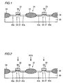
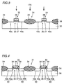
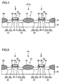
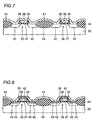
- Figs. 1 to 9 are sectional views for illustrating a manufacturing process for a semiconductor device according to an embodiment of the present invention.
- FIG. 1 A manufacturing process for a semiconductor device according to an embodiment of the present invention is now described with reference to Figs. 1 to 9.
- the present invention is applied to a manufacturing process for p-channel MOS transistors having a salicide structure.
- a second heat treatment is performed by RTA at a treatment temperature of about 700°C to about 800°C.
- the remaining conditions for the second heat treatment are identical to those for the first heat treatment.
- the temperature for this RTA is also less than 1000°C, dissimilarly to the RTA in the step 2.
- the titanium silicide films 42 pass into a C54 phase of low resistance from the C49 phase of high resistance due to the second heat treatment.
- the first and second field-effect transistors 35 and 36 manufactured in the aforementioned manner have a salicide structure.
- the sheet resistivity of the gate electrodes 38 having the titanium silicide films 42 on the surfaces and the source/drain regions 40 having the titanium silicide films 42 on the surfaces is reduced to about 3 ⁇ / ⁇ .
Landscapes
- Insulated Gate Type Field-Effect Transistor (AREA)
- Electrodes Of Semiconductors (AREA)
Applications Claiming Priority (4)
| Application Number | Priority Date | Filing Date | Title |
|---|---|---|---|
| JP5873799 | 1999-03-05 | ||
| JP5873799 | 1999-03-05 | ||
| JP2000024448 | 2000-02-01 | ||
| JP2000024448A JP2000323427A (ja) | 1999-03-05 | 2000-02-01 | 半導体装置の製造方法 |
Publications (2)
| Publication Number | Publication Date |
|---|---|
| EP1035565A2 true EP1035565A2 (de) | 2000-09-13 |
| EP1035565A3 EP1035565A3 (de) | 2004-07-07 |
Family
ID=26399759
Family Applications (1)
| Application Number | Title | Priority Date | Filing Date |
|---|---|---|---|
| EP00301383A Withdrawn EP1035565A3 (de) | 1999-03-05 | 2000-02-22 | Verfahren zur Herstellung eines Halbleiterbauelements mit einer Hoch-Temperatur Wärmebehandlung |
Country Status (5)
| Country | Link |
|---|---|
| US (1) | US6342440B1 (de) |
| EP (1) | EP1035565A3 (de) |
| JP (1) | JP2000323427A (de) |
| KR (1) | KR20000076772A (de) |
| CN (1) | CN1162896C (de) |
Families Citing this family (6)
| Publication number | Priority date | Publication date | Assignee | Title |
|---|---|---|---|---|
| US6890824B2 (en) * | 2001-08-23 | 2005-05-10 | Matsushita Electric Industrial Co., Ltd. | Semiconductor device and manufacturing method thereof |
| JP2003077854A (ja) * | 2001-09-05 | 2003-03-14 | Mitsubishi Electric Corp | 半導体装置の製造方法および半導体装置 |
| JP4594664B2 (ja) * | 2004-07-07 | 2010-12-08 | ルネサスエレクトロニクス株式会社 | 半導体装置の製造方法 |
| US20060068556A1 (en) * | 2004-09-27 | 2006-03-30 | Matsushita Electric Industrial Co., Ltd. | Semiconductor device and method for fabricating the same |
| JP4795759B2 (ja) * | 2005-03-03 | 2011-10-19 | ルネサスエレクトロニクス株式会社 | 電界効果型トランジスタの製造方法 |
| TWI620234B (zh) * | 2014-07-08 | 2018-04-01 | 聯華電子股份有限公司 | 一種製作半導體元件的方法 |
Family Cites Families (8)
| Publication number | Priority date | Publication date | Assignee | Title |
|---|---|---|---|---|
| JPS60119718A (ja) * | 1983-12-01 | 1985-06-27 | Nec Corp | 半導体装置の製造方法 |
| JP2527545B2 (ja) * | 1986-11-14 | 1996-08-28 | セイコーエプソン株式会社 | 半導体装置の製造方法 |
| JP3601232B2 (ja) * | 1996-02-26 | 2004-12-15 | ソニー株式会社 | 半導体装置の製造方法 |
| US5940699A (en) * | 1996-02-26 | 1999-08-17 | Sony Corporation | Process of fabricating semiconductor device |
| JPH1041407A (ja) | 1996-07-19 | 1998-02-13 | Sony Corp | 半導体装置の製造方法 |
| US5877050A (en) * | 1996-09-03 | 1999-03-02 | Advanced Micro Devices, Inc. | Method of making N-channel and P-channel devices using two tube anneals and two rapid thermal anneals |
| JPH1187258A (ja) * | 1997-09-09 | 1999-03-30 | Toshiba Corp | 半導体装置の製造方法 |
| US5981347A (en) * | 1997-10-14 | 1999-11-09 | Taiwan Semiconductor Manufacturing Company, Ltd. | Multiple thermal annealing method for a metal oxide semiconductor field effect transistor with enhanced hot carrier effect (HCE) resistance |
-
2000
- 2000-02-01 JP JP2000024448A patent/JP2000323427A/ja active Pending
- 2000-02-22 EP EP00301383A patent/EP1035565A3/de not_active Withdrawn
- 2000-03-03 CN CNB00103734XA patent/CN1162896C/zh not_active Expired - Fee Related
- 2000-03-03 US US09/518,246 patent/US6342440B1/en not_active Expired - Lifetime
- 2000-03-04 KR KR1020000010889A patent/KR20000076772A/ko not_active Withdrawn
Also Published As
| Publication number | Publication date |
|---|---|
| JP2000323427A (ja) | 2000-11-24 |
| US6342440B1 (en) | 2002-01-29 |
| EP1035565A3 (de) | 2004-07-07 |
| CN1162896C (zh) | 2004-08-18 |
| CN1266280A (zh) | 2000-09-13 |
| KR20000076772A (ko) | 2000-12-26 |
Similar Documents
| Publication | Publication Date | Title |
|---|---|---|
| US6436747B1 (en) | Method of fabricating semiconductor device | |
| JP2891092B2 (ja) | 半導体装置の製造方法 | |
| US7396767B2 (en) | Semiconductor structure including silicide regions and method of making same | |
| JP3348070B2 (ja) | 半導体装置の製造方法 | |
| KR101055708B1 (ko) | Cmos 기술에서 듀얼 살리사이드를 형성하는 방법 | |
| US6737710B2 (en) | Transistor structure having silicide source/drain extensions | |
| JPH11111980A (ja) | 半導体装置及びその製造方法 | |
| US6451679B1 (en) | Ion mixing between two-step titanium deposition process for titanium salicide CMOS technology | |
| KR0183490B1 (ko) | 반도체 소자의 제조 방법 | |
| US6518631B1 (en) | Multi-Thickness silicide device formed by succesive spacers | |
| JPH11284179A (ja) | 半導体装置およびその製造方法 | |
| US6342440B1 (en) | Method for forming low-leakage impurity regions by sequence of high-and low-temperature treatments | |
| JPH11186545A (ja) | シリサイド及びldd構造を有する半導体デバイスの製造方法 | |
| JP3295931B2 (ja) | 半導体装置の製造方法 | |
| KR100722936B1 (ko) | 모스 전계효과 트랜지스터 및 그 제조방법 | |
| JPH09199720A (ja) | Mos型半導体装置とその製造方法 | |
| JPH10209291A (ja) | Mos型半導体装置の製造方法 | |
| JPH10313117A (ja) | Misトランジスタ及びその製造方法 | |
| JPH06196687A (ja) | 半導体装置の製造方法 | |
| JPH10335645A (ja) | シリサイドを利用したスイッチング素子及びその製造方法 | |
| JPH11214328A (ja) | 半導体装置及びその製造方法 | |
| JPH0831949A (ja) | デュアルゲート構造cmos半導体装置とその製造方法 | |
| JP2000021996A (ja) | 半導体装置およびその製造方法 | |
| JPH11177103A (ja) | 半導体装置 | |
| JP3108927B2 (ja) | 半導体装置の製造方法 |
Legal Events
| Date | Code | Title | Description |
|---|---|---|---|
| PUAI | Public reference made under article 153(3) epc to a published international application that has entered the european phase |
Free format text: ORIGINAL CODE: 0009012 |
|
| 17P | Request for examination filed |
Effective date: 20000313 |
|
| AK | Designated contracting states |
Kind code of ref document: A2 Designated state(s): AT BE CH CY DE DK ES FI FR GB GR IE IT LI LU MC NL PT SE |
|
| AX | Request for extension of the european patent |
Free format text: AL;LT;LV;MK;RO;SI |
|
| RIC1 | Information provided on ipc code assigned before grant |
Ipc: 7H 01L 21/324 B Ipc: 7H 01L 21/8238 B Ipc: 7H 01L 21/336 B Ipc: 7H 01L 21/265 A |
|
| PUAL | Search report despatched |
Free format text: ORIGINAL CODE: 0009013 |
|
| AK | Designated contracting states |
Kind code of ref document: A3 Designated state(s): AT BE CH CY DE DK ES FI FR GB GR IE IT LI LU MC NL PT SE |
|
| AX | Request for extension of the european patent |
Extension state: AL LT LV MK RO SI |
|
| 17Q | First examination report despatched |
Effective date: 20050111 |
|
| AKX | Designation fees paid |
Designated state(s): DE FR GB IT NL |
|
| STAA | Information on the status of an ep patent application or granted ep patent |
Free format text: STATUS: THE APPLICATION IS DEEMED TO BE WITHDRAWN |
|
| 18D | Application deemed to be withdrawn |
Effective date: 20050522 |