EP1037054B1 - Structure étalon élémentaire à faibles pertes pour l'étalonnage d'une sonde de circuit intégré - Google Patents
Structure étalon élémentaire à faibles pertes pour l'étalonnage d'une sonde de circuit intégré Download PDFInfo
- Publication number
- EP1037054B1 EP1037054B1 EP00430005A EP00430005A EP1037054B1 EP 1037054 B1 EP1037054 B1 EP 1037054B1 EP 00430005 A EP00430005 A EP 00430005A EP 00430005 A EP00430005 A EP 00430005A EP 1037054 B1 EP1037054 B1 EP 1037054B1
- Authority
- EP
- European Patent Office
- Prior art keywords
- standard
- probe
- circuit
- circuits
- integrated circuit
- Prior art date
- Legal status (The legal status is an assumption and is not a legal conclusion. Google has not performed a legal analysis and makes no representation as to the accuracy of the status listed.)
- Expired - Lifetime
Links
Images


Classifications
-
- G—PHYSICS
- G01—MEASURING; TESTING
- G01R—MEASURING ELECTRIC VARIABLES; MEASURING MAGNETIC VARIABLES
- G01R35/00—Testing or calibrating of apparatus covered by the other groups of this subclass
- G01R35/005—Calibrating; Standards or reference devices, e.g. voltage or resistance standards, "golden" references
-
- G—PHYSICS
- G01—MEASURING; TESTING
- G01R—MEASURING ELECTRIC VARIABLES; MEASURING MAGNETIC VARIABLES
- G01R1/00—Details of instruments or arrangements of the types included in groups G01R5/00 - G01R13/00 and G01R31/00
- G01R1/28—Provision in measuring instruments for reference values, e.g. standard voltage, standard waveform
-
- H—ELECTRICITY
- H10—SEMICONDUCTOR DEVICES; ELECTRIC SOLID-STATE DEVICES NOT OTHERWISE PROVIDED FOR
- H10W—GENERIC PACKAGES, INTERCONNECTIONS, CONNECTORS OR OTHER CONSTRUCTIONAL DETAILS OF DEVICES COVERED BY CLASS H10
- H10W72/00—Interconnections or connectors in packages
- H10W72/90—Bond pads, in general
- H10W72/931—Shapes of bond pads
- H10W72/932—Plan-view shape, i.e. in top view
Definitions
- the present invention relates to the electrical test of so-called "RF" integrated circuits, with inputs or outputs provided for receiving or delivering signals alternatives in the field of radio frequencies.
- the present invention relates more particularly to electrical test of RF integrated circuits present on a silicon wafer, commonly called "wafer", before the cutting of the wafer into individual components.
- Figure 1 represents a wafer of silicon 1 on which has been made, by photolithography, a large number of integrated circuits 2 of same structure.
- an integrated circuit 2 has an active zone 3 and connection pads 4 electrically connected to the area active 3.
- Higher magnification of the active zone 3 would show hundreds or even thousands of integrated components together forming various functions electronic devices to be tested.
- the circuit electrical test integrated 2 still present on the wafer 1 to identify and to reject defective integrated circuits or those that do not present the expected characteristics, before the wafer cutting and assembly of integrated circuits individualized in a housing or their assembly on a interconnect support. This operation is therefore essential for reducing production costs, especially in the context of mass production.
- Figure 3 very schematically represents a system conventional wafer integrated circuit test, comprising a test station 11 connected to a probe 12 by through a bundle of electrical cables 13.
- the probe 12 is a printed circuit board 14 provided with metal tips arranged to coincide with the connection pads of an integrated circuit 2.
- the wafer 1 is disposed on a plate 16 movable in the horizontal plane and the integrated circuits are tested one after the other, by movements and movements of lifting and The entire system is piloted by a test program loaded into a memory 17, which determines the electrical characteristics of the signals of test to be applied to integrated circuits and the measurements to be carry out.
- This conventional method of testing integrated circuits in means of a probe constituted by a spiked card finds its limits when one wants to test RF integrated circuits comprising RF inputs / outputs requiring measurement frequencies ranging from a few hundred MegaHertz to some Gigahertz.
- These include integrated circuits with analog modulation functions and demodulation, mixers, amplifiers, filters, voltage controlled oscillators (VCOs), phase-locked loops (PLL) ..., intended for radio, television, radio receivers GPS receivers ...
- VCOs voltage controlled oscillators
- PLL phase-locked loops
- electrical signals have short wavelengths and we see appear in the probe 12 and in the drivers 13 connecting the probe to the test station 11 various phenomena of reflection and phase rotation that distort the measurements by creating interferences and changes in electrical levels.
- the tracks copper of the printed circuit board 14 and the tips 15 of the probe 12 have capacitances and inductances not insignificant parasites.
- RF probes satisfactory characteristics at high frequency.
- Cascade TM Microtech located at Oregon 97005, USA, proposes RF points ("transmission line probes") of reference “Air Coplanar” and membrane probes ("RFIC membrane probe cards ”) with HF conductors at microstrip (microstrip) and Nickel contact balls ("contact bumps").
- Such probes offer a band passing several tens of GigaHertz, a weak reflection coefficient S11 and a coefficient of S12 transmission with attenuation lower than 3dB (Cf. presentation of Cascade TM products on http // www.cmicro.com).
- the OSL method consists of carry out three measurements applying successively to the output of the probe at least three standard loads, in general infinite impedance (open circuit), zero impedance (short circuit), an impedance of 50 ⁇ (load).
- the network analyzer determines the parameters "S" of the probe and the test station performs, during subsequent measurements, automatic error correction to compensate for the influence of these parameters for obtaining accurate and reliable measurements.
- the standard loads used are thin layers on a ceramic substrate, calibrated by a National Metrology Laboratory.
- the RF points of the "Air Coplanar" type require manual adjustment of spike orientation and remain reserved for laboratory measurements or small productions.
- Membrane probes with balls of contact although specially designed for the test of integrated circuits on wafer, require to be calibrated the use of specific thin-layer standard circuits a high cost price. For various other reasons practices, the applicant considers that the probes membranes are not suitable for mass production of integrated circuits that can represent several million rooms.
- the tips or probes contact balls are forcefully applied on the connection ranges of the standard circuits, so that breaking a surface layer of oxide forming on contact air and establish a good electrical contact ("welding
- the thin-film standard circuits in addition to their high price, are therefore subject to wear and have a low lifetime.
- the thin-film standard circuits do not do not have the same thickness as silicon wafers and require for their installation a setting of the plateau 16 ( Figure 3) necessarily followed by another adjustment of the tray at the time of installation of the wafer.
- This inconvenience is compounded with the fact that RF probes require several calibrations during the test of a batch of fleas. These various calibrations involve the intervention of a qualified engineer and represent 5 to 10% of the time spent to the electrical test.
- a general objective of the present invention is to provide a method for calibrating an RF probe that is suitable for mass production, economical, simple to put implemented while being accurate and reliable, and who can may be implemented by unqualified personnel.
- a more particular object of the present invention is to provide a standard circuit which is of a low price of returns and simplifies calibration of a circuit probe RF integrated.
- a standard circuit comprising a plurality of elementary standard structures having standard charges of the same type, arranged in such a way as to have corresponding contact areas by their location to RF connection pads of the integrated circuit to test.
- the standard circuit includes a non-volatile memory connected to corresponding contact by their location to beaches of non-RF connection of the integrated circuit to be tested.
- a plate is also produced of silicon comprising a plurality of standard circuits according to the invention, or comprising both circuits integrated test and standard circuits according to the invention.
- each standard structure may be delimited laterally by engraving, or by furrows practiced in the substrate.
- one of the contact pads of a structure elementary standard is connected to the driver screen.
- an elementary standard structure may include two series standard loads connected by their point middle to the driver screen.
- a standard structure can also include at least one contact area to access in the middle point of the two standard loads.
- a standard load can be an open circuit formed by two sections of tracks conductors do not meet, a short circuit between two sections of conductive tracks, a resistive element connecting two sections of conductive tracks, or a capacity comprising a conductive plate deposited on the insulating layer and overhanging the buried conductor screen.
- RF integrated circuits are also realized comprising at least one conductive screen buried under two RF connection pads.
- the screen conductor may be delimited laterally by etching, or by grooves made in the circuit substrate integrated.
- a calibration method according to the invention of a test probe of an RF integrated circuit includes a step of determining the characteristics of the RF transmission lines of the probe made by means of a network analyzer and standard circuits according to the invention present on a silicon wafer.
- the present invention also relates to a method of electrical test of an RF integrated circuit present on a silicon wafer, by means of a test station provided with RF ports, a network analyzer and a probe, comprising a step of determining RF characteristics of the probe carried out by means of standard circuits according to the present invention on a silicon wafer, the RF characteristics of the probe being used as terms patches during the electrical test of the integrated circuit.
- the general objective of the invention is to perform the circuit electrical test embedded RF on silicon wafer in an environment industrial, in a simple, fast and inexpensive way by obtaining accurate and reliable measurements.
- the current invention includes various aspects that will be described each independently of each other.
- the electrical test of RF integrated circuits is carried out at by means of a probe 20 comprising a printed circuit 21 provided 22.
- the printed circuit board is shaped ring and the points 22, oriented towards the center of the structure, are arranged to coincide with the connection pads of an integrated circuit 50.
- the probe 20 is similar in structure to conventional circuit probes printed but has RF transmission lines offering satisfactory characteristics at high frequency. As as we will see later, these characteristics will be measured in the form of "S" parameters and compensated by the techniques classic error correction.
- the probe 20 constitutes an alternative to HF membrane probes, optional but advantageous in terms of flexibility of use and price cost, for measuring frequencies falling within the low of the RF range, ranging from a few hundred megahertz to some GigaHertz. Most RF ICs current operating in this frequency range, the probe 20 can cover almost all needs industrial.
- the printed circuit 21 is a multilayer circuit preferably having a ground plane 23 buried and uninterrupted, metallized crossings 24 to connect the various conductive levels, and RF-type connectors.
- the tips 22, of a short length of the order of 3 to 9 mm, are soldered by their base on the printed circuit 21 and are held by an electrically insulating piece 29 forming a kind of ring extending under the printed circuit 21.
- the printed circuit 21 has on its two faces of passive components 26, 27 as capabilities and inductors, allowing to match the impedances of transmission lines of the probe 20 connecting the connectors 25 to the spikes 22.
- the printed circuit 21 also includes transformers 28, for delivering symmetrical signals to test the differential inputs of a circuit integrated.
- Figure 6 shows the diagram of an embodiment of a line of transmission 30 provided for testing inputs differential of an integrated circuit ("balanced inputs").
- the line 30 comprises two conductive tracks 31, 32 of the circuit printed 21 leading to two points 22-1, 22-2.
- Tracks 31, 32 are connected to the terminals of the secondary coil of a transformer 28 whose midpoint is connected to the mass, the primary coil of the transformer being connected to a connector 25.
- the tracks 31, 32 each comprise a tuning capacity Ca1, Ca2 in series and are connected by a chord inductance La1.
- Capacities Ca1, Ca2 and the inductance La1 make it possible to compensate the influence parasitic elements present in the transmission line 30, in particular a parasitic capacitance Cp1 present between the transformer primary 27 and mass, capabilities parasites Cp2, Cp3 present between each terminal of the secondary and the mass, parasitic capacitances Cp4, Cp5 present between each point 22-1, 22-2 and the mass, and the inductances parasites Lp1, Lp2 of the points 22-1, 22-2. More particularly, the Ca1, Ca2 and inductance La1 make it possible to adjust the frequency of resonance of the transmission line 30 so that the probe 20 behaves like a "transparent window" allowing access to an integrated circuit.
- FIG. 7 shows the diagram of an embodiment of a line of unsymmetrical transmission 40 intended to test inputs unipolar of an integrated circuit ("single-ended inputs").
- the transmission line 40 includes a phase track 41 (signal) and a ground track 42 (reference) leading to points 22-3, 22-4.
- the tracks of phase 41 and mass 42 each have a Ca 3, Ca 4 series and are connected to ground by a La2 inductor, A3.
- these components make it possible compensate for the influence of parasitic elements Lp1, Lp2, Cp6 present in the transmission line.
- the coefficients S12 and S21 are considered equal.
- the "S" parameters of each of the lines RF transmission of the probe 20 will be determined at means of a network analyzer, after three measurements requiring to successively connect the spikes 22 to minus three standard loads Z1, Z2, Z3.
- the problem posed the calibration of the probe 20, and generally the calibration of an RF probe intended to be applied on a integrated circuit, is essentially practical and is related to number of transmission lines to be calibrated, and that multiple recalibrations are necessary during electrical test of a batch of integrated circuits.
- FIG. 9A represents a circuit integrated 50 having an active area 51 and ranges of aluminum connection.
- connection pads P1, P2, P3 ... P12 corresponding to RF inputs / outputs of the integrated circuit.
- These inputs / outputs can be of unipolar type ("single-ended") or of balanced type.
- Others connection pads, not referenced in the figure, are "non-RF" connection pads corresponding to I / O low frequency (logic signals) or current continuous (bias voltages, supply voltages, etc.).
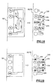
- FIG. 9B represents a standard circuit 60 according to the invention, made on a silicon substrate.
- the circuit 60 is a kind of dummy integrated circuit 50 not including the active area 51, in which there are the RF and non-RF connection pads of the integrated circuit 50.
- the connection pads P1 to P12 corresponding to the RF ranges of same reference of the circuit 50, are connected two by two to an elementary standard charge, respectively Z 1,2 , Z 3,4 , Z 5,6 , Z 7,8 , Z 9,10 , Z 11,12 .
- Non-RF ranges remain without connection.
- Each pair of tracks P1 / P2, P3 / P4,... P11 / P12 thus forms, with the reference charge Z associated therewith, an elemental reference structure on a silicon substrate, examples of which will be described below.
- FIG. 9C represents a variant embodiment in which the standard circuit, referenced 70, comprises in in addition to an active area 71 connected to the non-RF ranges.
- the area active 71 is a remanent type memory, for example a EEPROM memory comprising floating gate transistors, to store the values of standard loads elementary Z present across the RF ranges P1 to P12.
- the invention it is carried out on a silicon wafer at least three standard circuits 60 differing by the characteristic impedance of the Z standard loads they behave.
- the first standard circuit type "O" ("Open")
- the second circuit standard type “S” (“Short”)
- the third standard circuit of type "L” (“Load”)
- circuits are also provided.
- type "C1” and type “C2” standards, in which the Z loads are capacitors or inductances.
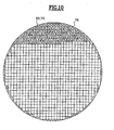
- Figures 10 and 11 illustrate two modes of realization of a wafer according to the invention.
- the wafer 75 includes only standard circuits 60 or 70 of type “O", “S”, “L”, “C1” and “C2" succeeding each other others and occupying all the useful surface of the wafer.
- the wafer 76 is a "production” wafer comprising integrated circuits 50 to be tested and marketed, as well as some 60 or 70 standard circuits arranged in place of certain integrated circuits 50.
- the wafer 76 has two rows five standard circuits of type "O", “S", “L” "C1” and “C2, taking the place of ten integrated circuits 50.
- circuits are thus available standards 60 or 70 (FIGS. 9B, 9C) of the same shape and likewise the size of the integrated circuits 50 to be tested (FIG. 9A), arranged on a wafer 75 of the same thickness as the wafer "production” ( Figure 10) or on the “production” wafer 76 itself ( Figure 11).
- These standard circuits include elementary standard structures with contact pads coinciding with the tips of the probe 20 ( Figure 4), dedicated to the electrical test of integrated circuits 50. As we will see below, these basic elementary structures go serve as "transfer standards" for bring them to the production sites, where the electrical test of integrated circuits is realized, a calibration reference given by calibrated thin-layer ceramic circuits by a national metrology laboratory.
- two RF peaks are calibrated 80 by means of a measuring bench 81 and a circuit 82 to thin layers having standard structures 83, 84, 85 type "O", "S", “L” calibrated by an approved laboratory.
- the tips 80 are for example Cascade TM Microtech tips the "Air Coplanar” series.
- the measuring bench 81 is provided with a conventional network analyzer, commonly available in the trade. The "S" parameters measured by the analyzer of network are used to calibrate the measurement system to the tips of the tips 80.
- the wafer 75 (FIG 10) is placed on the worktable and the RF peaks 80 measure the electrical characteristics of each elementary standard structure of each standard circuit 60 present on the wafer.
- the measurement is made at several frequencies, for example five frequencies, chosen according to the nominal frequency F0 of the integrated circuits to be tested later. For example, frequencies of 780, 790, 800, 810 and 820 MHz are chosen for integrated circuits having a nominal frequency of 800 MHz.
- the measurement bench 81 delivers the results of the measurements to a computer 86. These results are recorded on a support 87, for example a diskette, which will later accompany the wafer 75 on a production site.
- FIG. 14 schematically illustrates a variant of the calibration step in which the standard circuits 70 present on the wafer 75 each comprise a non-volatile memory 71, as described above in relation with FIG. 9C.
- the files containing the values of the elementary standard charges Z 1.2 .... Z 11.12 are stored in the memory 71 instead of being recorded on a diskette.
- the programming of the memory is done in a conventional manner, by means of a programmer 88 receiving the values to be recorded from the computer 86.
- the programmer 88 is connected to the non-RF contact pads of the circuit 70 by means of spikes 89.
- the standard wafer 75 is sent to a production site, which can be located thousands of kilometers from the place where it was calibrated.
- a production site which can be located thousands of kilometers from the place where it was calibrated.
- the probe 20 is connected to the RF and non-RF ports of the station 90 by coaxial cables or other types of cables.
- the cables connected to the RF ports are previously calibrated by the OSL method using standard commercially available loads.
- the probe 20 is calibrated by means of three standard circuits 60, 70 of type "O", "S” and "L" selected on the wafer 75 from the set of available standard circuits.
- the standard circuits are used only a specified number of times, for reasons relating to the degradation of the contact pads by the test points and the search for an optimal electrical contact.
- the values of the elementary standard impedances Z 1.2 , Z 3.4 ... Z 11.12 are given by the diskette 87 ( Figure 13) or are read directly into the integrated memory 71, by means of the probe 20.
- the data can also be transmitted via a computer network.
- the probe 20 is applied successively to three standard circuits, and station 90 measures the reflection coefficients ⁇ n of the various lines of RF transmission of the probe.
- the network analyzer of station 90 is able to determine the "S" parameters of the RF transmission lines of the probe. These parameters are kept in memory as corrective parameters of measurements made later during the electrical test of RF integrated circuits present on a "production" wafer.
- the calibration method according to the invention is simple and quick to implement. It only requires installing the wafer 75 on the test tray ("chuck") and the successive positioning of the probe 20 on three standard circuits.
- the process of the invention can be fully automated, and does not require intervention a qualified RF engineer.
- complementary standard circuits of type "C1" and “C2" verify the correct calibration of the probe and detect an isolated error. If the impedance values of "C1" and “C2" circuits measured with probe 20 do not do not correspond to the values given by the measuring bench reference number (FIG. 13 or 14), a signal can be generated alarm to make an operator intervene. The operator is going carry out a cleaning of the probe or a new calibration.
- FIG. 16A shows a sectional view of an "O" type elementary standard structure 100 (open circuit) produced on a silicon substrate 101, in particular a silicon wafer.
- the structure 100 comprises two contact pads 102, 103 deposited on the substrate 101 via an electrically insulating layer 104, for example silicon oxide. It is assumed here that the substrate is placed on a metal plate 105 connected to the ground.
- the application of a VRF voltage between the range 102 and the range 103 reveals an electric field E which radiates in the thickness of the substrate 101 and causes the standard structure to exhibit electrical losses.
- 16B shows that the ranges 102, 103, between which there is a resistor R0 representing the open circuit, are connected to the ground via a circuit C, R, L comprising a parasitic capacitance Cs1, the electrical resistance Rs1 of the substrate and a leakage inductance Ls1 of the metal plate 105 connected to the test equipment.
- the capacity Csl is of high value because its armatures are formed by the whole surface of the substrate, which extends well beyond the standard structure.
- Figure 17A is a sectional view of a structure 110 according to the invention, which differs from the previous in that a conductive screen 106 is buried under the oxide layer 104.
- the screen 106, metal, silicon polycrystalline or highly doped silicon is connected to the 104 (mass) by a conductive port 107 passing through the oxide layer, filled with metal or silicon strongly dope.
- the screen 106 extends over a limited area with regard to the surface of the substrate but underlie the whole area occupied by the standard structure, so that the beaches of contact 102, 103 overhang the screen 106.
- the field electrical E is confined between the range 102 and the screen 106 and electrical losses are diminished.
- FIG. 17B shows that the beach 102 is isolated from the substrate 101 and the metal tray 105.
- Beach 103 remains connected to the ground via Cs2 capacity, Rsl resistance and inductance Lsl of the metal tray 105.
- the capacity Cs2 is much lower than the capacity Csl of Figure 16B because its frames are defined by the size of the screen 106, which is much lower than that of the substrate.
- the standard structure 110 is therefore more satisfactory than the structure 100.
- Figures 18 and 19 show two structures elementary standards 120, 130 (right portion of the figures) and the initial arrangement of the connection pads on the circuit integrated 50 (left side of the figures).
- These structures standards 120, 130 are symmetrical and intended for the calibration of symmetrical transmission lines (figure 6), making it possible to test differential inputs of the integrated circuit. At the time of calibration of the probe, structures 120, 130 will thus receive a symmetrical signal.
- the "Air Coplanar" type RF tips used for calibrating the standard structures can not perform differential mode measurements, for reasons inherent to their HF structure.
- the standard structures 120, 130 solve this drawback, as we will see him now.
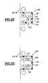
- the integrated circuit 50 for example includes a Vcc power supply range, a range GND, and two ranges P1, P2 corresponding to one differential input, schematically represented by a mounting two transistors T1, T2 to common emitter.
- the basic standard structure 120 includes the two ranges P1, P2 and is delimited by a conductive screen 121 buried under an insulating layer, including the edges are materialized by dashed lines.
- the P1, P2 are each connected to a load Z1, Z2 by sections of conductive tracks 122, 123.
- Charges Z1, Z2 are represented as a shape location square that can be left empty (open circuit) or receive a conductive material, for example an aluminum deposit of particular shape, wide or narrow (short circuit or resistance), or a resistive material such as doped silicon (resistance).
- the charges Z1, Z2 are connected to each other by a third section of track 124.
- the track section 124 is itself connected to the screen 106 by various conductive orifices 125 passing through the insulating layer.
- section 124 is extended in its central part in the form of an arm 126 leading to a GNDV virtual mass range, arranged between the beaches P1, P2, in alignment with the latter.
- the load Z1 is first measured by placing the points (80) on the P1 and GNDV ranges. We then measure the Z2 load via the P2 and GNDV ranges. The elementary standard charge for the calibration of a line of differential transmission is calculated by doing the sum two charges Z1 and Z2.
- the elementary structure 130 of FIG. distinguished from the structure 120 by the fact that two ranges of virtual mass GNDV1, GNDV2 are arranged in relation to P1 and P2, on the other side of the charges Z1, Z2, the P1 and P2 ranges being too close to each other for allow insertion of a measuring range.
- the section of track 124 connects the GNDV1, GNDV2 and extends beyond of these to follow the area occupied by the screen 121 and guarantee a good connection to the latter, thanks to various conducting orifices 125.
- the load Z1 is measured between the ranges P1 and GNDV1 and the load Z2 is measured between the P2 and GNDV2 ranges.
- Fig. 20 shows a symmetrical standard structure 160 of type "C1" or “C2".
- This structure looks like strongly to an "S" type structure that would be realized in accordance with Figure 18, the elementary charges being formed by squares of conductive material, or plates 161, 162, connected to the ranges P1, P2.
- the plates 161, 162 do not come into contact with the section of central track 163 (runway section 163, connected to the buried screen 164, is preserved because the structure 160 is performed in the same way as a structure of type "O", "S” or “L”).
- the plates 161, 162 form with the buried driver screen 164 two capacitors in series Ca, Cb.
- the total impedance of structure 160 is a capacitor whose value depends on the size of the plates 161, 162.
- Figure 22 shows a standard structure elementary element 140 of unsymmetrical type, in which the P1 range is intended to receive the phase and the range P2 to receive the mass of a measurement signal.
- the P1 range is connected to a load Z3 by a section of track 141 and the P2 range is connected to the other end of the Z3 load by a section of runway 142.
- Runway section 142 is connected to a buried driver screen 143 via of conducting orifices 144, arranged in particular along a arm 145 along the area occupied by the screen 143.
- Figure 23 shows a symmetrical structure 150 in which the range P1 is connected by a section of track 151 to a Z4 load and the P2 range is connected by a track section 152 at a load Z5.
- a section of track 153 connects the charges Z4, Z5 whose sum forms the impedance standard.
- the track section 153 is connected to a buried screen 154, by orifices 155.
- the screen 154 thus forms a virtual mass, although the structure does not has no virtual mass range.
- Non-capacitive type capacitive structures symmetric can also be achieved by following the teaching of Figure 20, charges Z3, or Z4 and Z5 then taking the form of conductive plates connected only at P1, P2.
- structures inductive effects can be achieved by means of metal shaped flat coils.
- the standard structures according to the invention are preferably made using the same technology than the corresponding integrated circuit.
- the technology called "HSB2" High Speed Bipolar
- HSD2 High Speed Bipolar
- furrows are practiced all around each standard structure according to the invention for cutting the buried conductive layer, and show under each elemental structure a conductive screen insulated from the rest of the conductive layer.
- a another embodiment, in itself more conventional, is to burn the buried layer before the deposit of the oxide layer, so that only the conductive screens.
- a standard circuit according to the invention has electrical properties that are as close as possible to those of the integrated circuit to be tested. So, he enters the of the present invention to provide circuits integrated circuits, for example the circuit 50 of FIG. 9A, having under each pair of RF ranges a conductive screen.
- the forecasting such a screen can only improve the performance of the high-frequency circuit, reducing its electrical losses.
- the screen is arranged as illustrated by one of FIGS. 18 to 23, according to which the tracks of the circuit integrated correspond to symmetrical inputs / outputs or unsymmetrical.
- the screen can be connected to the range of mass in the case of an unsymmetrical input.
- the screen In the case of a differential input, the screen can be connected to the midpoint of the load seen from the connection pads. This midpoint is for example the connection point of the transmitters of transistors T1, T2 shown in FIG. 18.
- the first aspect of the invention relates to the use of optional RF probe made from a circuit printed, replacing conventional membrane probes.
- the second aspect relates to the realization of circuits standards on silicon with coinciding contact pads with the connection pads of an integrated circuit to be tested and, therefore, with the tips or the balls of contact a probe for testing the integrated circuit.
- the third aspect of the invention relates to the calibration a test probe by means of these standard circuits, used as transfer standards.
- the fourth aspect of the invention relates to the production of structures Low-loss silicon standards with a display buried, and to the generalization of the screen buried at RF integrated circuits themselves.
- the fifth aspect of the invention relates to embodiments of elementary standard structures, including structures symmetrical with additional contact areas to be calibrated with unsymmetrical RF tips. he it will be clear to those skilled in the art that these various aspects of the invention are independent of one another, although their combination forms an advantageous whole to achieve in the most direct way the general objective of the invention.
Landscapes
- Physics & Mathematics (AREA)
- General Physics & Mathematics (AREA)
- Testing Or Measuring Of Semiconductors Or The Like (AREA)
- Semiconductor Integrated Circuits (AREA)
- Testing Of Individual Semiconductor Devices (AREA)
Description
- la figure 1 précédemment décrite représente une plaquette ou "wafer" de silicium comprenant des circuits intégrés,
- la figure 2 représente un circuit intégré présent sur le wafer de la figure 1,
- la figure 3 représente un système de test classique de circuit intégré non-RF,
- la figure 4 est une vue de dessus d'une sonde de circuit intégré RF selon l'invention,
- la figure 5 est une vue en coupe de la sonde selon l'invention,
- les figures 6 et 7 sont des schémas électriques de lignes de transmission RF de la sonde selon l'invention,
- la figure 8 illustre une modélisation sous forme de réseau RF d'une ligne de transmission RF,
- la figure 9A représente un circuit intégré RF et les figures 9B et 9C représentent deux circuits étalons,
- les figures 10 et 11 représentent des wafer de silicium comportant des circuits étalons selon l'invention,
- les figures 12, 13, 14 et 15 illustrent un procédé d'étalonnage selon l'invention d'une sonde de test RF,
- les figures 16A et 17A sont des vues en coupe de deux structures étalons élémentaires et illustrent un aspect de l'invention,
- les figures 16B et 17B sont des schémas électriques des structures étalons des figures 16A et 17A,
- les figures 18, 19, 20, 22 et 23 représentent par des vues de dessus divers modes de réalisation de structures étalons élémentaires selon l'invention, et
- la figure 21 est une vue en coupe de la structure étalon de la figure 20.
| exemples de fichiers : | ||||
| Circuit | Type | Fichier | Fréquence de mesure | Mesures |
| Circuit étalon N° 1 | "O" ("open") | Fichier de Z1,2 | F0 | Γ = 0.95 ϕ = -15° |
| F0+10MHz | Γ = 0.94 ϕ = -16° | |||
| F0-10MHz | Γ = 0.96 ϕ = -14° | |||
| F0+20MHz | Γ = 0.93 ϕ = -17° | |||
| F0-20MHz | Γ = 0.97 ϕ = -13° | |||
| Fichier de Z3,4 | F0 | Γ = 0.95 ϕ = -15° | ||
| F0+10MHz | Γ = 0.95 ϕ = -16° | |||
| F0-10MHz | Γ = 0.95 ϕ = -14° | |||
| F0+20MHz | Γ = 0.95 ϕ = -17° | |||
| F0-20MHz | Γ = 0.96 ϕ = -13° | |||
| ... | ... | ... | ||
| Fichier de Z11,12 | F0 | Γ = 0.95 ϕ = -15° | ||
| F0+10MHz | Γ = 0.95 ϕ = -16° | |||
| F0-10MHz | Γ = 0.95 ϕ = -14° | |||
| F0+20MHz | Γ = 0.94 ϕ = -17° | |||
| F0-20MHz | Γ = 0.96 ϕ = -14° | |||
| Circuit étalon N° 2 | "S" ("short") | Fichier de Z1,2 | F0 | Γ = 0.98 ϕ = +20° |
| F0+10MHz | Γ = 0.97 ϕ = +25° | |||
| ... | ... | |||
| Fichier de Z3,4 | ... | ... | ||
| ... | ... | ... | ||
| Fichier de Z11,12 | ... | ... | ||
| Circuit étalon N° 3 ...(etc.) | "L" ("Load") ... | Fichier de Z1,2 | F0 | Γ = 0.02 ϕ = +21° |
| ... | ||||
| ... | ... | ... | ||
| ... | ... | ... |
Claims (16)
- Structure étalon élémentaire (110, 120, 130, 140, 150, 160) pour la détermination des caractéristiques RF d'une sonde (20) de circuit intégré RF, caractérisée en ce qu'elle comprend au moins deux plages de contact (P1, P2, GNDV, GNDV1, GNDV2) déposées sur un substrat de silicium (101) par l'intermédiaire d'une couche électriquement isolante (104), au moins une charge étalon (Z1, Z2, Z3, Z4, Z5, Ca, Cb) mesurable depuis les plages de contact, et un écran conducteur (106, 121, 143, 154, 164) enterré sous la couche isolante.
- Structure étalon selon la revendication 1, dans laquelle l'écran conducteur (106, 121, 143, 154, 164) est délimité latéralement par gravure.
- Structure étalon selon la revendication 1, dans laquelle l'écran conducteur (106, 121, 143, 154, 164) est délimité latéralement par des sillons pratiqués dans le substrat.
- Structure étalon selon l'une des revendications 1 à 3, dans laquelle l'une des plages de contact (P2, GNDV, GNDV1, GNDV2) est connectée à l'écran conducteur.
- Structure étalon selon l'une des revendications 1 à 3, comprenant deux charges étalons (Z1, Z2, Z4, Z5, Ca, Cb) en série connectées par leur point milieu à l'écran conducteur.
- Structure étalon selon la revendication 5, comprenant au moins une plage de contact (GNDV, GNDV1, GNDV2) pour accéder au point milieu des deux charges étalons.
- Structure étalon selon l'une des revendications 1 à 6, dans laquelle une charge étalon est un circuit ouvert formé par deux tronçons de pistes conductrices (122, 123, 141, 142) ne se rejoignant pas.
- Structure étalon selon l'une des revendications 1 à 6, dans laquelle une charge étalon est un court-circuit entre deux tronçons de pistes conductrices (122, 123, 141, 142).
- Structure étalon selon l'une des revendications 1 à 6, dans laquelle une charge étalon est un élément résistif reliant deux tronçons de pistes conductrices (122, 123, 141, 142).
- Structure étalon (160) selon l'une des revendications 1 à 6, dans laquelle une charge étalon est une capacité (Ca, Cb) comprenant une plaque conductrice (161, 162) déposée sur la couche isolante et surplombant l'écran conducteur enterré (164).
- Circuit étalon (60, 70) pour la mesure des caractéristiques RF d'une sonde (20) de test d'un circuit intégré RF, caractérisé en ce qu'il comprend une pluralité de structures étalons élémentaires selon l'une des revendications 1 à 10, ayant des charges étalons de même type ("O", "S", "L", "C1", "C2") agencées de manière à présenter des plages de contact (P1-P12) correspondant par leur emplacement à des plages de connexion RF du circuit intégré (50) à tester.
- Circuit étalon (70) selon la revendication 11, comprenant en outre une mémoire rémanente (71) connectée à des plages de contact du circuit étalon correspondant par leur emplacement à des plages de connexion non-RF du circuit intégré (50) à tester.
- Plaquette de silicium (75), comprenant une pluralité de circuits étalons (60, 70) selon l'une des revendications 11 et 12.
- Plaquette de silicium (76), comprenant à la fois des circuits intégrés à tester (50) et des circuits étalons (60, 70) selon l'une des revendications 11 et 12.
- Procédé d'étalonnage d'une sonde (20) de test d'un circuit intégré RF (50), comprenant une étape de détermination, au moyen d'un analyseur de réseau (90) et de circuits étalons, des caractéristiques des lignes de transmission RF (30, 40) de la sonde, caractérisé en ce que l'étape de détermination est réalisée au moyen de circuits étalons (60, 70) présents sur une plaquette de silicium (75, 76) selon l'une des revendications 13 et 14.
- Procédé de test électrique d'un circuit intégré RF (50) présent sur une plaquette de silicium, au moyen d'une station de test (90) pourvue de ports RF, d'un analyseur de réseau et d'une sonde (20), caractérisé en ce qu'il comprend une étape de détermination des caractéristiques RF de la sonde (20) réalisée conformément au procédé de la revendication 15, et en ce que les caractéristiques RF de la sonde (20) sont utilisées comme termes correctifs au cours du test électrique du circuit intégré.
Applications Claiming Priority (2)
| Application Number | Priority Date | Filing Date | Title |
|---|---|---|---|
| FR9902197A FR2790096B1 (fr) | 1999-02-18 | 1999-02-18 | Structure etalon elementaire a faibles pertes pour l'etalonnage d'une sonde de circuit integre |
| FR9902197 | 1999-02-18 |
Publications (2)
| Publication Number | Publication Date |
|---|---|
| EP1037054A1 EP1037054A1 (fr) | 2000-09-20 |
| EP1037054B1 true EP1037054B1 (fr) | 2005-07-27 |
Family
ID=9542384
Family Applications (1)
| Application Number | Title | Priority Date | Filing Date |
|---|---|---|---|
| EP00430005A Expired - Lifetime EP1037054B1 (fr) | 1999-02-18 | 2000-02-10 | Structure étalon élémentaire à faibles pertes pour l'étalonnage d'une sonde de circuit intégré |
Country Status (4)
| Country | Link |
|---|---|
| US (1) | US6423981B1 (fr) |
| EP (1) | EP1037054B1 (fr) |
| DE (1) | DE60021457D1 (fr) |
| FR (1) | FR2790096B1 (fr) |
Families Citing this family (10)
| Publication number | Priority date | Publication date | Assignee | Title |
|---|---|---|---|---|
| US7250626B2 (en) * | 2003-10-22 | 2007-07-31 | Cascade Microtech, Inc. | Probe testing structure |
| MX2007000156A (es) * | 2004-07-02 | 2007-06-15 | Research In Motion Ltd | Acceso de pruebad de rf para probar antena en dispositivo de comunicacion movil. |
| US7130032B2 (en) * | 2005-03-11 | 2006-10-31 | Northrop Grumman Corporation | Alternate test method for RF cable testing to avoid long test cables |
| US20060224345A1 (en) * | 2005-04-04 | 2006-10-05 | Ives Fred H | System and method for improving electrical equipment accuracy by environmental condition compensation |
| US7323948B2 (en) * | 2005-08-23 | 2008-01-29 | International Business Machines Corporation | Vertical LC tank device |
| KR100819561B1 (ko) * | 2007-01-12 | 2008-04-08 | 삼성전자주식회사 | 반도체 장치 및 이 장치의 신호 종단 방법 |
| DE102007027155A1 (de) * | 2007-04-03 | 2008-10-23 | Rohde & Schwarz Gmbh & Co. Kg | Wellenleiter-System mit differenziellem Wellenleiter |
| US7994801B2 (en) * | 2007-05-08 | 2011-08-09 | Tektronix, Inc. | Calibrated S-parameter measurements of a high impedance probe |
| WO2018163167A1 (fr) * | 2017-03-06 | 2018-09-13 | Jerusalem College Of Technology | Redresseur intégré |
| CN114814699B (zh) * | 2022-05-16 | 2025-06-17 | 浙江大学 | 一种结构内嵌的在片校准件及其校准测试方法 |
Family Cites Families (9)
| Publication number | Priority date | Publication date | Assignee | Title |
|---|---|---|---|---|
| JPS6164138A (ja) * | 1984-09-06 | 1986-04-02 | Nec Corp | モノリシツク集積回路 |
| DE3502713A1 (de) * | 1985-01-28 | 1986-07-31 | Robert Bosch Gmbh, 7000 Stuttgart | Monolithisch integrierte schaltung mit untertunnelung |
| JPS6341041A (ja) * | 1986-08-06 | 1988-02-22 | Mitsubishi Electric Corp | 半導体装置 |
| JPH02168674A (ja) * | 1988-12-21 | 1990-06-28 | Mitsubishi Electric Corp | 不揮発性半導体記憶装置 |
| US4994737A (en) * | 1990-03-09 | 1991-02-19 | Cascade Microtech, Inc. | System for facilitating planar probe measurements of high-speed interconnect structures |
| US5684301A (en) * | 1994-04-28 | 1997-11-04 | The United States Of America As Represented By The Secretary Of Commerce | Monocrystalline test structures, and use for calibrating instruments |
| JP2570147B2 (ja) * | 1993-11-18 | 1997-01-08 | 日本電気株式会社 | 半導体装置 |
| JP3376731B2 (ja) * | 1994-11-09 | 2003-02-10 | 東京エレクトロン株式会社 | 高周波用のプリント基板及びこれを用いたプローブカード |
| JP2900908B2 (ja) * | 1997-03-31 | 1999-06-02 | 日本電気株式会社 | 半導体装置およびその製造方法 |
-
1999
- 1999-02-18 FR FR9902197A patent/FR2790096B1/fr not_active Expired - Fee Related
-
2000
- 2000-02-10 EP EP00430005A patent/EP1037054B1/fr not_active Expired - Lifetime
- 2000-02-10 DE DE60021457T patent/DE60021457D1/de not_active Expired - Lifetime
- 2000-02-18 US US09/507,991 patent/US6423981B1/en not_active Expired - Lifetime
Also Published As
| Publication number | Publication date |
|---|---|
| US6423981B1 (en) | 2002-07-23 |
| DE60021457D1 (de) | 2005-09-01 |
| FR2790096A1 (fr) | 2000-08-25 |
| EP1037054A1 (fr) | 2000-09-20 |
| FR2790096B1 (fr) | 2001-04-13 |
Similar Documents
| Publication | Publication Date | Title |
|---|---|---|
| EP1030182A1 (fr) | Procédé d'étalonnage d'une sonde de circuit integré RF | |
| EP1037054B1 (fr) | Structure étalon élémentaire à faibles pertes pour l'étalonnage d'une sonde de circuit intégré | |
| FR2790842A1 (fr) | Procede de fabrication d'un circuit de test sur une plaquette de silicium | |
| US4764723A (en) | Wafer probe | |
| US7071707B2 (en) | Method for calibrating and de-embedding, set of devices for de-embedding and vector network analyzer | |
| FR2733598A1 (fr) | Sonde de tension a plusieurs conducteurs | |
| JP4870211B2 (ja) | 差動信号用テスト構造及びプローブ | |
| US7723999B2 (en) | Calibration structures for differential signal probing | |
| FR2823568A1 (fr) | Procede et appareil pour l'etalonnage des supports des testeurs de circuits integres | |
| KR0153390B1 (ko) | 기생 캐패시터의 영향을 감소시킬 수 있는 반도체 회로 소자 | |
| FR2780162A1 (fr) | Structure de test de circuit, circuit integre et procede de test | |
| Walk et al. | Characterization and deembedding of negative series inductance in on-wafer measurements of thin-film all-oxide varactors | |
| WO2023104737A1 (fr) | Système et procédé de test d'une mémoire à résistance variable | |
| EP0273825B1 (fr) | Dispositif de mesure des caractéristiques d'un composant hyperfréquence | |
| EP0053213B1 (fr) | Nouveau condensateur à structure de quadripôle dont l'intégrité peut être contrôlée à l'aide de tests en courant continu | |
| CH692162A5 (fr) | Procédé de mesure pour détecter un court-circuit entre des spires d'une bobine intégrée sur une puce, et structure de circuit intégré adaptée à un tel procédé de mesure. | |
| FR2892521A1 (fr) | Systeme de mesure de permeabilite magnetique et echantillon de reference utilise dans celui-ci | |
| EP0596773A1 (fr) | Dispositif pour tests hyperfréquences à large bande réalisés in situ | |
| FR2696009A1 (fr) | Dispositif de calibrage pour ajuster en hyperfréquence les plans de référence d'un appareillage de mesure des paramètres de dispersion d'éléments de circuits intégrés. | |
| US7427802B2 (en) | Irreversible reduction of the value of a polycrystalline silicon resistor | |
| JP3971627B2 (ja) | 中間層回路の特性評価方法 | |
| EP0042319B1 (fr) | Amplificateur linéaire hybride ultra-rapide | |
| KR20100066024A (ko) | 금속-절연체-금속 커패시터의 고주파영역대 품질계수 측정 테스트 패턴 및 측정방법 | |
| FR2644896A1 (fr) | Carte a pointes pour le test des composants semi-conducteurs hyperfrequences | |
| WO1990008327A2 (fr) | Systeme d'interface de mesure par un analyseur logique des signaux numeriques d'un circuit integre |
Legal Events
| Date | Code | Title | Description |
|---|---|---|---|
| PUAI | Public reference made under article 153(3) epc to a published international application that has entered the european phase |
Free format text: ORIGINAL CODE: 0009012 |
|
| AK | Designated contracting states |
Kind code of ref document: A1 Designated state(s): DE FR GB IT |
|
| AX | Request for extension of the european patent |
Free format text: AL;LT;LV;MK;RO;SI |
|
| 17P | Request for examination filed |
Effective date: 20010131 |
|
| AKX | Designation fees paid |
Free format text: DE FR GB IT |
|
| RAP1 | Party data changed (applicant data changed or rights of an application transferred) |
Owner name: STMICROELECTRONICS S.A. |
|
| RAP1 | Party data changed (applicant data changed or rights of an application transferred) |
Owner name: STMICROELECTRONICS SA |
|
| 17Q | First examination report despatched |
Effective date: 20040315 |
|
| GRAP | Despatch of communication of intention to grant a patent |
Free format text: ORIGINAL CODE: EPIDOSNIGR1 |
|
| GRAS | Grant fee paid |
Free format text: ORIGINAL CODE: EPIDOSNIGR3 |
|
| GRAA | (expected) grant |
Free format text: ORIGINAL CODE: 0009210 |
|
| AK | Designated contracting states |
Kind code of ref document: B1 Designated state(s): DE FR GB IT |
|
| PG25 | Lapsed in a contracting state [announced via postgrant information from national office to epo] |
Ref country code: IT Free format text: LAPSE BECAUSE OF FAILURE TO SUBMIT A TRANSLATION OF THE DESCRIPTION OR TO PAY THE FEE WITHIN THE PRESCRIBED TIME-LIMIT;WARNING: LAPSES OF ITALIAN PATENTS WITH EFFECTIVE DATE BEFORE 2007 MAY HAVE OCCURRED AT ANY TIME BEFORE 2007. THE CORRECT EFFECTIVE DATE MAY BE DIFFERENT FROM THE ONE RECORDED. Effective date: 20050727 |
|
| REG | Reference to a national code |
Ref country code: GB Ref legal event code: FG4D Free format text: NOT ENGLISH |
|
| REF | Corresponds to: |
Ref document number: 60021457 Country of ref document: DE Date of ref document: 20050901 Kind code of ref document: P |
|
| PG25 | Lapsed in a contracting state [announced via postgrant information from national office to epo] |
Ref country code: DE Free format text: LAPSE BECAUSE OF FAILURE TO SUBMIT A TRANSLATION OF THE DESCRIPTION OR TO PAY THE FEE WITHIN THE PRESCRIBED TIME-LIMIT Effective date: 20051028 |
|
| GBT | Gb: translation of ep patent filed (gb section 77(6)(a)/1977) |
Effective date: 20051116 |
|
| PLBE | No opposition filed within time limit |
Free format text: ORIGINAL CODE: 0009261 |
|
| STAA | Information on the status of an ep patent application or granted ep patent |
Free format text: STATUS: NO OPPOSITION FILED WITHIN TIME LIMIT |
|
| 26N | No opposition filed |
Effective date: 20060428 |
|
| PGFP | Annual fee paid to national office [announced via postgrant information from national office to epo] |
Ref country code: GB Payment date: 20080129 Year of fee payment: 9 |
|
| PGFP | Annual fee paid to national office [announced via postgrant information from national office to epo] |
Ref country code: FR Payment date: 20080228 Year of fee payment: 9 |
|
| GBPC | Gb: european patent ceased through non-payment of renewal fee |
Effective date: 20090210 |
|
| REG | Reference to a national code |
Ref country code: FR Ref legal event code: ST Effective date: 20091030 |
|
| PG25 | Lapsed in a contracting state [announced via postgrant information from national office to epo] |
Ref country code: FR Free format text: LAPSE BECAUSE OF NON-PAYMENT OF DUE FEES Effective date: 20090302 Ref country code: GB Free format text: LAPSE BECAUSE OF NON-PAYMENT OF DUE FEES Effective date: 20090210 |