EP1039713A2 - Réduction de délai dans des récepteurs de signaux multiporteuse - Google Patents
Réduction de délai dans des récepteurs de signaux multiporteuse Download PDFInfo
- Publication number
- EP1039713A2 EP1039713A2 EP00105963A EP00105963A EP1039713A2 EP 1039713 A2 EP1039713 A2 EP 1039713A2 EP 00105963 A EP00105963 A EP 00105963A EP 00105963 A EP00105963 A EP 00105963A EP 1039713 A2 EP1039713 A2 EP 1039713A2
- Authority
- EP
- European Patent Office
- Prior art keywords
- circuit
- estimating
- carrier frequency
- signal
- synchronization
- Prior art date
- Legal status (The legal status is an assumption and is not a legal conclusion. Google has not performed a legal analysis and makes no representation as to the accuracy of the status listed.)
- Granted
Links
Images



Classifications
-
- H—ELECTRICITY
- H04—ELECTRIC COMMUNICATION TECHNIQUE
- H04L—TRANSMISSION OF DIGITAL INFORMATION, e.g. TELEGRAPHIC COMMUNICATION
- H04L27/00—Modulated-carrier systems
- H04L27/26—Systems using multi-frequency codes
- H04L27/2601—Multicarrier modulation systems
- H04L27/2647—Arrangements specific to the receiver only
- H04L27/2655—Synchronisation arrangements
- H04L27/2657—Carrier synchronisation
-
- H—ELECTRICITY
- H04—ELECTRIC COMMUNICATION TECHNIQUE
- H04L—TRANSMISSION OF DIGITAL INFORMATION, e.g. TELEGRAPHIC COMMUNICATION
- H04L27/00—Modulated-carrier systems
- H04L27/26—Systems using multi-frequency codes
- H04L27/2601—Multicarrier modulation systems
- H04L27/2647—Arrangements specific to the receiver only
- H04L27/2655—Synchronisation arrangements
- H04L27/2662—Symbol synchronisation
-
- H—ELECTRICITY
- H04—ELECTRIC COMMUNICATION TECHNIQUE
- H04L—TRANSMISSION OF DIGITAL INFORMATION, e.g. TELEGRAPHIC COMMUNICATION
- H04L27/00—Modulated-carrier systems
- H04L27/26—Systems using multi-frequency codes
- H04L27/2601—Multicarrier modulation systems
- H04L27/2647—Arrangements specific to the receiver only
- H04L27/2655—Synchronisation arrangements
- H04L27/2668—Details of algorithms
- H04L27/2673—Details of algorithms characterised by synchronisation parameters
- H04L27/2675—Pilot or known symbols
Definitions
- the present invention relates to an OFDM (Orthogonal Frequency Division Multiplexing) demodulator of a burst signal transfer system using an OFDM modulating method and, more particularly, to an OFDM demodulator in which a processing delay of a synchronization circuit can be shortened.
- OFDM Orthogonal Frequency Division Multiplexing
- An OFDM modulating method as a modulating method promising for a high-speed data transfer such as a high-speed wireless LAN has been being examined.
- a conventional OFDM demodulator for receiving an OFDM modulated signal will be described by referring to drawings.
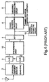
- Fig. 4 is a block diagram showing the configuration of a conventional OFDM demodulator.
- Fig. 5 is a diagram showing a format of an OFDM burst signal.
- a preamble 21 for symbol synchronization and a preamble 22 for estimating a carrier frequency and a channel characteristic are provided.
- an OFDM burst signal is received by an antenna 1.
- An orthogonal component detector 2 performs quasi-synchronous detection (QUASI-SYNC) on the received signal by using a local signal having a frequency which is very close to a carrier frequency to thereby obtain an analog complex baseband signal.
- QASI-SYNC quasi-synchronous detection
- A/D converters 3 and 4 sample and quantize an analog complex baseband signal of an orthogonal component and an in-phase component outputted from the orthogonal component detector 2.
- a synchronization circuit 10 receives a digital complex baseband signal sampled and quantized by the A/D converters 3 and 4 and performs a synchronizing operation.
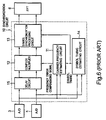
- Fig. 6 is a block diagram showing the synchronization circuit 10.
- a symbol timing estimating circuit 14 which receives the digital complex baseband signal establishes symbol synchronization by the digital complex baseband signal sampled and quantized which is outputted from the A/D converters 3 and 4 at the time of receiving the preamble 21 for symbol synchronization shown in Fig. 5.
- the symbol timing estimating circuit 14 outputs a symbol timing to a carrier frequency estimating circuit 11 and a symbol synchronization processing circuit 13.
- the carrier frequency estimating circuit 11 On receipt of the preamble 22 for estimating the carrier frequency and channel characteristic having repetitive patterns, the carrier frequency estimating circuit 11 detects phase rotation in the same patterns which periodically appears, estimates a carrier frequency error, and outputs a frequency error compensating signal to a complex multiplier 12.
- a specific configuration of a carrier frequency estimating circuit is described in, for example, F. Daffara and O. Adami, "A new frequency detector for orthogonal multicarrier transmission techniques" Proc. of VTC' 95, pp 804 - 809.
- a delay circuit 15 receives the digital complex baseband signal, delays the signal by predetermined time (which is about time of the preamble 22 for estimating the carrier frequency and channel characteristic) and, supplies the resultant signal to the complex multiplier 12.
- the complex multiplier 12 complex-multiplies the frequency error compensated signal by the output of the delay circuit 15, thereby compensating a frequency deviation of the carrier wave.
- the preamble 22 for estimating the carrier frequency/channel characteristic is outputted from the synchronization circuit 10.
- a fast Fourier transform (FFT) circuit 6 in Fig. 4 Fourier transforms an output signal of a synchronization circuit 5 and divides the OFDM modulated signal into signals of subcarriers.
- FFT fast Fourier transform
- a channel distortion estimating circuit 16 On receipt of the preamble 22, a channel distortion estimating circuit 16 receives the signals of subcarriers from the FFT circuit 6 and estimates a channel characteristic H( ⁇ ).
- the preamble 22 for estimating the carrier frequency/channel characteristic is used to estimate the channel characteristic H( ⁇ ) in the channel distortion estimating circuit 16.
- the channel distortion estimating circuit 16 outputs a coefficient 1/H( ⁇ ) for compensating channel distortion to a channel distortion compensating circuit 8.
- the channel distortion compensating circuit 8 receives the signals of respective subcarriers and compensates the channel distortion by complex-multiplying the signal by the coefficient 1/H( ⁇ ) for compensating the channel distortion.
- Fig. 7 is a block diagram of the channel distortion estimating circuit 16.
- the preamble signal 22 for estimating the carrier frequency/channel characteristics is supplied to a complex multiplier 161 in the channel distortion estimating circuit 16.
- the inverse number of the pattern of the preamble signal 22 is stored in a reference signal storing circuit 163 and is supplied to the other input terminal of the complex multiplier 161 in the channel distortion estimating circuit 16.
- Both input signals are multiplied by each other in the complex multiplier 161 and an estimation result H( ⁇ ) of the channel characteristic is obtained as an output of the complex multiplier 161.
- the output H( ⁇ ) of the complex multiplier 161 is supplied to an inverse number circuit 162 and a coefficient 1/H( ⁇ ) for compensating the channel distortion is computed.
- the coefficient 1/H( ⁇ ) is multiplied by an output of the FFT 6 in the complex multiplier 8, thereby compensating the channel distortion.
- a subcarrier demodulating circuit 9 receives the distortion compensating signal and demodulates it every subcarrier.
- the conventional OFDM demodulator has the delay circuit 15 in the synchronization circuit 10 used for compensating the carrier frequency deviation with respect to the preamble for estimating the carrier frequency and channel characteristic.
- OFDM orthogonal frequency division multiplexing
- an orthogonal frequency division multiplexing (OFDM) demodulator for demodulating an OFDM modulated signal, comprising: a quasi-synchronous detector for converting the OFDM modulated signal into a complex baseband signal of two components by quasi-synchronous detection; a synchronization circuit for receiving the complex baseband signal and establishing symbol synchronization; an FFT for Fourier transforming an output of the synchronization circuit into signals of respective subcarriers; a channel distortion estimating circuit for compensating a carrier frequency error on the basis of an output of the FFT and a frequency error compensation signal outputted from the synchronization circuit and estimating channel distortion; a channel distortion compensating circuit for compensating channel distortion in the output of the FFT on the basis of an output of the channel distortion estimating circuit; and a demodulating circuit for demodulating an output of the channel distortion compensating circuit every subcarrier.
- OFDM orthogonal frequency division multiplexing
- a frequency error compensation signal is detected by using a preamble signal for estimating carrier frequency/channel characteristic in a carrier frequency estimating circuit in a synchronization circuit having no delay circuit.
- the frequency error compensation signal is outputted to a complex multiplier in a propagation path distortion estimating circuit. After phase rotation caused by a frequency error is corrected by an output of the complex multiplier, the channel distortion is estimated and compensated.
- the carrier frequency deviation is not compensated in the synchronization at the front stage of the FFT but is compensated after the FFT.
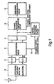
- Fig. 1 is a block diagram showing the configuration of an OFDM demodulator of the invention.
- the format of an OFDM burst signal is as shown in Fig. 5.
- an OFDM burst signal is received by the antenna 1.
- the orthogonal component detector 2 converts the reception signal into an analog complex baseband signal by using a local signal of a frequency which is very close to the carrier frequency by quasi-synchronous detection (QUASI-SYNC).
- QUASI-SYNC quasi-synchronous detection
- the A/D converters 3 and 4 sample and quantize the analog complex baseband signal of an orthogonal component and an in-phase component outputted from the orthogonal component detector 2.
- the synchronization circuit 5 receives a sampled and quantized digital complex baseband signal outputted from the A/D converters 3 and 4 and performs a synchronizing operation.
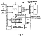
- Fig. 2 shows the configuration of the synchronization circuit 5.
- the symbol timing estimating circuit 14 establishes symbol synchronization by the sampled and quantized digital complex baseband signal outputted from the A/D converters 3 and 4 at the time of receiving the preamble 21 for symbol synchronization.
- the symbol timing estimating circuit 14 outputs a symbol timing to the carrier frequency estimating circuit 15 and the symbol synchronization processing circuit 13.
- the carrier frequency estimating circuit 15 On receipt of the preamble 22 for estimating the carrier frequency and transmission path having repetitive patterns, the carrier frequency estimating circuit 15 detects phase rotation in the same pattern which periodically appears, estimates a carrier frequency error, and outputs it as a frequency error compensating signal 16 to a channel distortion estimating circuit 7. On the other hand, the carrier frequency estimating circuit 15 outputs the result as another output.
- the delay circuit 15 is provided at the front stage of the complex multiplier 12.
- the preamble 22 passes through the complex multiplier 12 before the result of estimation of the carrier frequency is obtained. In the synchronization circuit 5 of the invention, therefore, the frequency is not compensated in the period of the preamble 22.
- the preamble 22 is outputted from the synchronization circuit 5.
- the frequency error compensating signal 16 is supplied from the carrier frequency estimating circuit 15 to the complex multiplier 12 where the frequency is compensated.
- the symbol timing is outputted to the symbol synchronization processing circuit 13 and a symbol synchronizing process is performed.
- the fast Fourier transform (FFT) circuit 6 in Fig. 1 performs Fourier transform on the output signal of the synchronization circuit 5 to divide the OFDM modulation signal into signals of subcarriers.
- the channel distortion estimating circuit 7 On receipt of the preamble 22, the channel distortion estimating circuit 7 receives the signals of respective subcarriers from the FFT circuit 6 and estimates a channel characteristic H( ⁇ ).
- the carrier frequency is compensated by frequency error information from the synchronization circuit 5 in the channel distortion estimating circuit 7 and then the preamble 22 is used to estimate the channel characteristic H( ⁇ ).
- the channel distortion estimating circuit 7 outputs a coefficient 1/H( ⁇ ) for compensating channel distortion to the channel distortion compensating circuit 8.
- the channel distortion compensating circuit 8 receives the signals of respective subcarriers and compensates the channel distortion by complex-multiplying the signal by the coefficient 1/H( ⁇ ) for compensating the channel distortion.
- Fig. 3 is a block diagram of the channel distortion estimating circuit 7.
- the preamble signal 22 for estimating carrier frequency and channel characteristic is supplied to a complex multiplier 71 in the channel distortion estimating circuit 7.
- the frequency error compensation signal 10 outputted from the synchronization circuit 5 is also supplied to the complex multiplier 71.
- phase rotation caused by a frequency error is corrected by using the frequency error information from the frequency error compensation signal 10.
- An output of the complex multiplier 71 is multiplied by an output of a reference signal storing circuit 74 in which the inverse number of the pattern of the preamble 22 is stored by a complex multiplier 72, thereby obtaining a channel distortion estimation result H( ⁇ ).
- the output H( ⁇ ) of the complex multiplier 72 is supplied to an inverse number circuit 75 where a coefficient 1/H( ⁇ ) for compensating the channel distortion is calculated.
- the channel distortion compensating coefficient 1/H( ⁇ ) is multiplied by an output of the FFT 6 by the complex multiplier 8, thereby compensating the channel distortion.
- the subcarrier demodulating circuit 9 receives the distortion compensating signal and demodulates it every subcarrier.
- a reception signal is first subjected to orthogonal component detection and a resultant is A/D converted.
- a resultant is A/D converted.
- the compensation of the carrier frequency deviation of the preamble for estimating the carrier frequency and the channel characteristic is not performed in the synchronization circuit but is performed after the FFT.
Landscapes
- Engineering & Computer Science (AREA)
- Computer Networks & Wireless Communication (AREA)
- Signal Processing (AREA)
- Synchronisation In Digital Transmission Systems (AREA)
- Digital Transmission Methods That Use Modulated Carrier Waves (AREA)
- Radio Transmission System (AREA)
Applications Claiming Priority (2)
| Application Number | Priority Date | Filing Date | Title |
|---|---|---|---|
| JP8456099 | 1999-03-26 | ||
| JP8456099 | 1999-03-26 |
Publications (3)
| Publication Number | Publication Date |
|---|---|
| EP1039713A2 true EP1039713A2 (fr) | 2000-09-27 |
| EP1039713A3 EP1039713A3 (fr) | 2003-11-12 |
| EP1039713B1 EP1039713B1 (fr) | 2006-05-31 |
Family
ID=13834045
Family Applications (1)
| Application Number | Title | Priority Date | Filing Date |
|---|---|---|---|
| EP00105963A Expired - Lifetime EP1039713B1 (fr) | 1999-03-26 | 2000-03-24 | Réduction de délai dans des récepteurs de signaux multiporteuse |
Country Status (3)
| Country | Link |
|---|---|
| US (1) | US6680901B1 (fr) |
| EP (1) | EP1039713B1 (fr) |
| DE (1) | DE60028276T2 (fr) |
Cited By (1)
| Publication number | Priority date | Publication date | Assignee | Title |
|---|---|---|---|---|
| US7474611B2 (en) | 2005-04-21 | 2009-01-06 | Telefonaktiebolaget L M Ericsson (Publ) | Reduced complexity channel estimation in OFDM systems |
Families Citing this family (21)
| Publication number | Priority date | Publication date | Assignee | Title |
|---|---|---|---|---|
| EP1236326A1 (fr) * | 1999-11-27 | 2002-09-04 | Deutsche Telekom AG | Recepteur et procede d'annulation de l'interference entre voies dans un systeme de communication a ondes porteuses multiples |
| EP1821480B1 (fr) | 2000-08-24 | 2009-10-21 | Sony Deutschland Gmbh | Système de communication pour la réception et la transmission de signaux OFDM dans un système de communications sans fil |
| JP3776716B2 (ja) * | 2000-11-17 | 2006-05-17 | 株式会社東芝 | 直交周波数分割多重伝送信号受信装置 |
| WO2002063341A1 (fr) * | 2001-02-02 | 2002-08-15 | Dbi Corporation | Telemetrie de fond et systeme de commande |
| US7136432B2 (en) * | 2001-06-08 | 2006-11-14 | Broadcom Corporation | Robust burst detection and acquisition system and method |
| US7139340B2 (en) * | 2002-06-28 | 2006-11-21 | Hitachi, Ltd. | Robust OFDM carrier recovery methods and apparatus |
| KR100823252B1 (ko) * | 2002-11-07 | 2008-04-21 | 삼성전자주식회사 | Ofdm 기반 동기 검출 장치 및 방법 |
| TWI381702B (zh) * | 2003-06-17 | 2013-01-01 | Semiconductor Energy Lab | 具有攝像功能之顯示裝置及雙向通訊系統 |
| EP1983673B1 (fr) * | 2006-02-06 | 2012-09-05 | Sony Corporation | Dispositif, méthode et programme de démodulation |
| US9083573B2 (en) | 2008-10-15 | 2015-07-14 | Stmicroelectronics Asia Pacific Pte. Ltd. | Simultaneous transmission of signals, such as orthogonal-frequency-division-multiplexed (OFDM) signals, that include a same frequency |
| US9020050B2 (en) * | 2008-10-15 | 2015-04-28 | Stmicroelectronics, Inc. | Accounting for inter-carrier interference in determining a response of an OFDM communication channel |
| US9338033B2 (en) | 2008-10-15 | 2016-05-10 | Stmicroelectronics, Inc. | Recovering data from a primary one of simultaneous signals, such as orthogonal-frequency-division-multiplexed (OFDM) signals, that include a same frequency |
| US9148311B2 (en) | 2008-10-15 | 2015-09-29 | Stmicroelectronics, Inc. | Determining responses of rapidly varying MIMO-OFDM communication channels using observation scalars |
| US9596106B2 (en) | 2008-10-15 | 2017-03-14 | Stmicroelectronics, Inc. | Pilot pattern for observation-scalar MIMO-OFDM |
| US9130788B2 (en) | 2008-10-15 | 2015-09-08 | Stmicroelectronics, Inc. | Determining a response of a rapidly varying OFDM communication channel using an observation scalar |
| US9137054B2 (en) | 2008-10-15 | 2015-09-15 | Stmicroelectronics, Inc. | Pilot pattern for MIMO OFDM |
| US9130789B2 (en) | 2008-10-15 | 2015-09-08 | Stmicroelectronics Asia Pacific Pte. Ltd. | Recovering data from a secondary one of simultaneous signals, such as orthogonal-frequency-division-multiplexed (OFDM) signals, that include a same frequency |
| US9240908B2 (en) | 2008-10-15 | 2016-01-19 | Stmicroelectronics, Inc. | Pilot pattern for observation scalar MIMO-OFDM |
| US8718208B2 (en) * | 2008-10-15 | 2014-05-06 | Stmicroelectronics, Inc. | Recovery of data from a multi carrier signal |
| JP5347792B2 (ja) * | 2009-07-16 | 2013-11-20 | ソニー株式会社 | 信号処理装置、信号処理方法、及び、受信システム |
| US9693240B2 (en) * | 2015-05-29 | 2017-06-27 | Interdigital Technology Corporation | Methods and apparatuses for advanced receiver design |
Family Cites Families (5)
| Publication number | Priority date | Publication date | Assignee | Title |
|---|---|---|---|---|
| SE504787C2 (sv) * | 1994-12-14 | 1997-04-28 | Hd Divine Ab | Metod vid OFDM-mottagning för korrigering av frekvens, tidsfönster, samplingsklocka och långsamma fasvariationer |
| US5682376A (en) * | 1994-12-20 | 1997-10-28 | Matsushita Electric Industrial Co., Ltd. | Method of transmitting orthogonal frequency division multiplex signal, and transmitter and receiver employed therefor |
| US5802117A (en) * | 1996-02-08 | 1998-09-01 | Philips Electronics North America Corporation | Method and apparatus for joint frequency offset and timing estimation of a multicarrier modulation system |
| JPH10257013A (ja) * | 1997-03-14 | 1998-09-25 | Toshiba Corp | 受信装置 |
| US6175550B1 (en) * | 1997-04-01 | 2001-01-16 | Lucent Technologies, Inc. | Orthogonal frequency division multiplexing system with dynamically scalable operating parameters and method thereof |
-
2000
- 2000-03-24 EP EP00105963A patent/EP1039713B1/fr not_active Expired - Lifetime
- 2000-03-24 DE DE60028276T patent/DE60028276T2/de not_active Expired - Lifetime
- 2000-03-27 US US09/534,535 patent/US6680901B1/en not_active Expired - Lifetime
Cited By (1)
| Publication number | Priority date | Publication date | Assignee | Title |
|---|---|---|---|---|
| US7474611B2 (en) | 2005-04-21 | 2009-01-06 | Telefonaktiebolaget L M Ericsson (Publ) | Reduced complexity channel estimation in OFDM systems |
Also Published As
| Publication number | Publication date |
|---|---|
| US6680901B1 (en) | 2004-01-20 |
| EP1039713B1 (fr) | 2006-05-31 |
| EP1039713A3 (fr) | 2003-11-12 |
| DE60028276T2 (de) | 2007-05-03 |
| DE60028276D1 (de) | 2006-07-06 |
Similar Documents
| Publication | Publication Date | Title |
|---|---|---|
| US6680901B1 (en) | OFDM demodulator | |
| EP1041790B1 (fr) | Synchronisation de symbole pour démodulateur OFDM | |
| US7039000B2 (en) | Timing synchronization for OFDM-based wireless networks | |
| EP2315386B1 (fr) | Procédés et appareil de communication OFDM | |
| US6731594B1 (en) | Transmission system for OFDM-signals with optimized synchronisation | |
| KR100807886B1 (ko) | 직교 주파수 분할 다중화 시스템의 수신 장치 | |
| US7283598B2 (en) | OFDM receiver apparatus | |
| EP0851642B1 (fr) | Récepteur de signaux multiporteurs, à compensation de décalages en fréquence et de distortions qui dépendent de fréquence | |
| JP2001094524A (ja) | 通信システム、送信装置、受信装置、送信方法、受信方法、および、情報記録媒体 | |
| EP1195961A2 (fr) | Correction de décalages en fréquence dans des récepteurs multiporteuses | |
| EP1193934B1 (fr) | Corrections de décalages de fréquence dans des récepteurs multiporteuses | |
| US7158476B2 (en) | OFDM receiver using polar coordinate system and method thereof | |
| JP3555843B2 (ja) | 復調装置 | |
| JP3544147B2 (ja) | Ofdm信号受信装置、ofdm信号通信システム及びその通信制御方法 | |
| JP3946893B2 (ja) | ディジタル通信装置 | |
| JP3339490B2 (ja) | Ofdm復調装置 | |
| JP3495962B2 (ja) | 歪み推定装置 | |
| JPH07154129A (ja) | Lms方式のアダプティブアレイアンテナ装置 | |
| JP3583013B2 (ja) | 復調装置 | |
| JP2000022660A (ja) | ディジタル通信装置 | |
| KR20020086161A (ko) | 직교 주파수 분할 다중 전송 시스템의 훈련 심볼 결정방법 및 주파수 옵셋 추정과 동기를 위한 장치 및 방법 | |
| JP3616550B2 (ja) | Ofdm復調装置 | |
| JP4779279B2 (ja) | 受信装置及び受信方法 | |
| KR100195748B1 (ko) | 직교 주파수 분할 다중 수신 시스템 | |
| USRE43829E1 (en) | Transmission system for OFDM-signals with optimized synchronization |
Legal Events
| Date | Code | Title | Description |
|---|---|---|---|
| PUAI | Public reference made under article 153(3) epc to a published international application that has entered the european phase |
Free format text: ORIGINAL CODE: 0009012 |
|
| AK | Designated contracting states |
Kind code of ref document: A2 Designated state(s): AT BE CH CY DE DK ES FI FR GB GR IE IT LI LU MC NL PT SE |
|
| AX | Request for extension of the european patent |
Free format text: AL;LT;LV;MK;RO;SI |
|
| PUAL | Search report despatched |
Free format text: ORIGINAL CODE: 0009013 |
|
| AK | Designated contracting states |
Kind code of ref document: A3 Designated state(s): AT BE CH CY DE DK ES FI FR GB GR IE IT LI LU MC NL PT SE |
|
| AX | Request for extension of the european patent |
Extension state: AL LT LV MK RO SI |
|
| 17P | Request for examination filed |
Effective date: 20031002 |
|
| AKX | Designation fees paid |
Designated state(s): DE NL SE |
|
| 17Q | First examination report despatched |
Effective date: 20040624 |
|
| GRAP | Despatch of communication of intention to grant a patent |
Free format text: ORIGINAL CODE: EPIDOSNIGR1 |
|
| GRAS | Grant fee paid |
Free format text: ORIGINAL CODE: EPIDOSNIGR3 |
|
| GRAA | (expected) grant |
Free format text: ORIGINAL CODE: 0009210 |
|
| AK | Designated contracting states |
Kind code of ref document: B1 Designated state(s): DE NL SE |
|
| PG25 | Lapsed in a contracting state [announced via postgrant information from national office to epo] |
Ref country code: NL Free format text: LAPSE BECAUSE OF FAILURE TO SUBMIT A TRANSLATION OF THE DESCRIPTION OR TO PAY THE FEE WITHIN THE PRESCRIBED TIME-LIMIT Effective date: 20060531 |
|
| REF | Corresponds to: |
Ref document number: 60028276 Country of ref document: DE Date of ref document: 20060706 Kind code of ref document: P |
|
| PG25 | Lapsed in a contracting state [announced via postgrant information from national office to epo] |
Ref country code: SE Free format text: LAPSE BECAUSE OF FAILURE TO SUBMIT A TRANSLATION OF THE DESCRIPTION OR TO PAY THE FEE WITHIN THE PRESCRIBED TIME-LIMIT Effective date: 20060831 |
|
| NLV1 | Nl: lapsed or annulled due to failure to fulfill the requirements of art. 29p and 29m of the patents act | ||
| PLBE | No opposition filed within time limit |
Free format text: ORIGINAL CODE: 0009261 |
|
| STAA | Information on the status of an ep patent application or granted ep patent |
Free format text: STATUS: NO OPPOSITION FILED WITHIN TIME LIMIT |
|
| 26N | No opposition filed |
Effective date: 20070301 |
|
| PGFP | Annual fee paid to national office [announced via postgrant information from national office to epo] |
Ref country code: DE Payment date: 20130320 Year of fee payment: 14 |
|
| REG | Reference to a national code |
Ref country code: DE Ref legal event code: R119 Ref document number: 60028276 Country of ref document: DE |
|
| REG | Reference to a national code |
Ref country code: DE Ref legal event code: R119 Ref document number: 60028276 Country of ref document: DE Effective date: 20141001 |
|
| PG25 | Lapsed in a contracting state [announced via postgrant information from national office to epo] |
Ref country code: DE Free format text: LAPSE BECAUSE OF NON-PAYMENT OF DUE FEES Effective date: 20141001 |