EP1047042A2 - Appareil d'affichage à plasma et méthode de commande d'un tel appareil - Google Patents
Appareil d'affichage à plasma et méthode de commande d'un tel appareil Download PDFInfo
- Publication number
- EP1047042A2 EP1047042A2 EP99309449A EP99309449A EP1047042A2 EP 1047042 A2 EP1047042 A2 EP 1047042A2 EP 99309449 A EP99309449 A EP 99309449A EP 99309449 A EP99309449 A EP 99309449A EP 1047042 A2 EP1047042 A2 EP 1047042A2
- Authority
- EP
- European Patent Office
- Prior art keywords
- erase
- discharge
- cell
- period
- pulse
- Prior art date
- Legal status (The legal status is an assumption and is not a legal conclusion. Google has not performed a legal analysis and makes no representation as to the accuracy of the status listed.)
- Withdrawn
Links
Images


Classifications
-
- G—PHYSICS
- G09—EDUCATION; CRYPTOGRAPHY; DISPLAY; ADVERTISING; SEALS
- G09G—ARRANGEMENTS OR CIRCUITS FOR CONTROL OF INDICATING DEVICES USING STATIC MEANS TO PRESENT VARIABLE INFORMATION
- G09G3/00—Control arrangements or circuits, of interest only in connection with visual indicators other than cathode-ray tubes
- G09G3/20—Control arrangements or circuits, of interest only in connection with visual indicators other than cathode-ray tubes for presentation of an assembly of a number of characters, e.g. a page, by composing the assembly by combination of individual elements arranged in a matrix no fixed position being assigned to or needed to be assigned to the individual characters or partial characters
- G09G3/22—Control arrangements or circuits, of interest only in connection with visual indicators other than cathode-ray tubes for presentation of an assembly of a number of characters, e.g. a page, by composing the assembly by combination of individual elements arranged in a matrix no fixed position being assigned to or needed to be assigned to the individual characters or partial characters using controlled light sources
- G09G3/28—Control arrangements or circuits, of interest only in connection with visual indicators other than cathode-ray tubes for presentation of an assembly of a number of characters, e.g. a page, by composing the assembly by combination of individual elements arranged in a matrix no fixed position being assigned to or needed to be assigned to the individual characters or partial characters using controlled light sources using luminous gas-discharge panels, e.g. plasma panels
- G09G3/288—Control arrangements or circuits, of interest only in connection with visual indicators other than cathode-ray tubes for presentation of an assembly of a number of characters, e.g. a page, by composing the assembly by combination of individual elements arranged in a matrix no fixed position being assigned to or needed to be assigned to the individual characters or partial characters using controlled light sources using luminous gas-discharge panels, e.g. plasma panels using AC panels
- G09G3/291—Control arrangements or circuits, of interest only in connection with visual indicators other than cathode-ray tubes for presentation of an assembly of a number of characters, e.g. a page, by composing the assembly by combination of individual elements arranged in a matrix no fixed position being assigned to or needed to be assigned to the individual characters or partial characters using controlled light sources using luminous gas-discharge panels, e.g. plasma panels using AC panels controlling the gas discharge to control a cell condition, e.g. by means of specific pulse shapes
- G09G3/292—Control arrangements or circuits, of interest only in connection with visual indicators other than cathode-ray tubes for presentation of an assembly of a number of characters, e.g. a page, by composing the assembly by combination of individual elements arranged in a matrix no fixed position being assigned to or needed to be assigned to the individual characters or partial characters using controlled light sources using luminous gas-discharge panels, e.g. plasma panels using AC panels controlling the gas discharge to control a cell condition, e.g. by means of specific pulse shapes for reset discharge, priming discharge or erase discharge occurring in a phase other than addressing
-
- G—PHYSICS
- G09—EDUCATION; CRYPTOGRAPHY; DISPLAY; ADVERTISING; SEALS
- G09G—ARRANGEMENTS OR CIRCUITS FOR CONTROL OF INDICATING DEVICES USING STATIC MEANS TO PRESENT VARIABLE INFORMATION
- G09G3/00—Control arrangements or circuits, of interest only in connection with visual indicators other than cathode-ray tubes
- G09G3/20—Control arrangements or circuits, of interest only in connection with visual indicators other than cathode-ray tubes for presentation of an assembly of a number of characters, e.g. a page, by composing the assembly by combination of individual elements arranged in a matrix no fixed position being assigned to or needed to be assigned to the individual characters or partial characters
- G09G3/2007—Display of intermediate tones
- G09G3/2018—Display of intermediate tones by time modulation using two or more time intervals
- G09G3/2022—Display of intermediate tones by time modulation using two or more time intervals using sub-frames
-
- G—PHYSICS
- G09—EDUCATION; CRYPTOGRAPHY; DISPLAY; ADVERTISING; SEALS
- G09G—ARRANGEMENTS OR CIRCUITS FOR CONTROL OF INDICATING DEVICES USING STATIC MEANS TO PRESENT VARIABLE INFORMATION
- G09G3/00—Control arrangements or circuits, of interest only in connection with visual indicators other than cathode-ray tubes
- G09G3/20—Control arrangements or circuits, of interest only in connection with visual indicators other than cathode-ray tubes for presentation of an assembly of a number of characters, e.g. a page, by composing the assembly by combination of individual elements arranged in a matrix no fixed position being assigned to or needed to be assigned to the individual characters or partial characters
- G09G3/22—Control arrangements or circuits, of interest only in connection with visual indicators other than cathode-ray tubes for presentation of an assembly of a number of characters, e.g. a page, by composing the assembly by combination of individual elements arranged in a matrix no fixed position being assigned to or needed to be assigned to the individual characters or partial characters using controlled light sources
- G09G3/28—Control arrangements or circuits, of interest only in connection with visual indicators other than cathode-ray tubes for presentation of an assembly of a number of characters, e.g. a page, by composing the assembly by combination of individual elements arranged in a matrix no fixed position being assigned to or needed to be assigned to the individual characters or partial characters using controlled light sources using luminous gas-discharge panels, e.g. plasma panels
- G09G3/288—Control arrangements or circuits, of interest only in connection with visual indicators other than cathode-ray tubes for presentation of an assembly of a number of characters, e.g. a page, by composing the assembly by combination of individual elements arranged in a matrix no fixed position being assigned to or needed to be assigned to the individual characters or partial characters using controlled light sources using luminous gas-discharge panels, e.g. plasma panels using AC panels
- G09G3/291—Control arrangements or circuits, of interest only in connection with visual indicators other than cathode-ray tubes for presentation of an assembly of a number of characters, e.g. a page, by composing the assembly by combination of individual elements arranged in a matrix no fixed position being assigned to or needed to be assigned to the individual characters or partial characters using controlled light sources using luminous gas-discharge panels, e.g. plasma panels using AC panels controlling the gas discharge to control a cell condition, e.g. by means of specific pulse shapes
- G09G3/292—Control arrangements or circuits, of interest only in connection with visual indicators other than cathode-ray tubes for presentation of an assembly of a number of characters, e.g. a page, by composing the assembly by combination of individual elements arranged in a matrix no fixed position being assigned to or needed to be assigned to the individual characters or partial characters using controlled light sources using luminous gas-discharge panels, e.g. plasma panels using AC panels controlling the gas discharge to control a cell condition, e.g. by means of specific pulse shapes for reset discharge, priming discharge or erase discharge occurring in a phase other than addressing
- G09G3/2927—Details of initialising
-
- G—PHYSICS
- G09—EDUCATION; CRYPTOGRAPHY; DISPLAY; ADVERTISING; SEALS
- G09G—ARRANGEMENTS OR CIRCUITS FOR CONTROL OF INDICATING DEVICES USING STATIC MEANS TO PRESENT VARIABLE INFORMATION
- G09G3/00—Control arrangements or circuits, of interest only in connection with visual indicators other than cathode-ray tubes
- G09G3/20—Control arrangements or circuits, of interest only in connection with visual indicators other than cathode-ray tubes for presentation of an assembly of a number of characters, e.g. a page, by composing the assembly by combination of individual elements arranged in a matrix no fixed position being assigned to or needed to be assigned to the individual characters or partial characters
- G09G3/22—Control arrangements or circuits, of interest only in connection with visual indicators other than cathode-ray tubes for presentation of an assembly of a number of characters, e.g. a page, by composing the assembly by combination of individual elements arranged in a matrix no fixed position being assigned to or needed to be assigned to the individual characters or partial characters using controlled light sources
- G09G3/28—Control arrangements or circuits, of interest only in connection with visual indicators other than cathode-ray tubes for presentation of an assembly of a number of characters, e.g. a page, by composing the assembly by combination of individual elements arranged in a matrix no fixed position being assigned to or needed to be assigned to the individual characters or partial characters using controlled light sources using luminous gas-discharge panels, e.g. plasma panels
- G09G3/288—Control arrangements or circuits, of interest only in connection with visual indicators other than cathode-ray tubes for presentation of an assembly of a number of characters, e.g. a page, by composing the assembly by combination of individual elements arranged in a matrix no fixed position being assigned to or needed to be assigned to the individual characters or partial characters using controlled light sources using luminous gas-discharge panels, e.g. plasma panels using AC panels
- G09G3/296—Driving circuits for producing the waveforms applied to the driving electrodes
-
- G—PHYSICS
- G09—EDUCATION; CRYPTOGRAPHY; DISPLAY; ADVERTISING; SEALS
- G09G—ARRANGEMENTS OR CIRCUITS FOR CONTROL OF INDICATING DEVICES USING STATIC MEANS TO PRESENT VARIABLE INFORMATION
- G09G2310/00—Command of the display device
- G09G2310/06—Details of flat display driving waveforms
- G09G2310/066—Waveforms comprising a gently increasing or decreasing portion, e.g. ramp
-
- G—PHYSICS
- G09—EDUCATION; CRYPTOGRAPHY; DISPLAY; ADVERTISING; SEALS
- G09G—ARRANGEMENTS OR CIRCUITS FOR CONTROL OF INDICATING DEVICES USING STATIC MEANS TO PRESENT VARIABLE INFORMATION
- G09G2320/00—Control of display operating conditions
- G09G2320/02—Improving the quality of display appearance
- G09G2320/0228—Increasing the driving margin in plasma displays
-
- G—PHYSICS
- G09—EDUCATION; CRYPTOGRAPHY; DISPLAY; ADVERTISING; SEALS
- G09G—ARRANGEMENTS OR CIRCUITS FOR CONTROL OF INDICATING DEVICES USING STATIC MEANS TO PRESENT VARIABLE INFORMATION
- G09G2320/00—Control of display operating conditions
- G09G2320/02—Improving the quality of display appearance
- G09G2320/0238—Improving the black level
Definitions
- the present invention relates to an AC driving type plasma display driving method and Apparatus.
- PDPs plasma display panels
- AC driving type PDP that can realize a large screen, is expected as a display device coping with high-quality digital broadcasting, and is demanded to attain higher image quality than the CRT.
- Fig. 1 is a circuit diagram showing the whole arrangement of an AC driving type PDP apparatus.
- an AC driving type PDP 1 comprises scanning electrodes Y1 to Yn and common electrodes X parallel to each other on one surface, and address electrodes A1 to Am perpendicular to these electrodes Y1 to Yn and X on the opposing surface.
- the common electrodes X are laid out close to the scanning electrodes Y1 to Yn in correspondence with them, and have terminals commonly connected.
- the common terminal of the common electrodes X is connected to the output terminal of an X driver 2, the scanning electrodes Y1 to Yn are connected to the output terminals of a Y driver 3, and the address electrodes A1 to Am are connected to the output terminals of an address driver 4.
- the X driver 2, Y driver 3, and address driver 4 are controlled by control signals from a controller 5.
- the controller 5 generates the control signals on the basis of external display data D, clock CLK indicating the read timing of the display data D, horizontal sync signal HS, and vertical sync signal VS, and supplies the control signals to the X driver 2, Y driver 3, and address driver 4.
- Fig. 2 is a sectional view showing the structure of a cell Cij as one pixel on the i-th row and j-th column.
- a common electrode X and a scanning electrode Yi are formed on a front glass substrate 11.
- the common electrode X and scanning electrode Yi are covered with a dielectric layer 12 for insulating them from a discharge space 17, and the dielectric layer 12 is covered with a MgO (magnesium oxide) protective film 13.
- An address electrode Aj is formed on a rear glass substrate 14 facing the front glass substrate 11, and covered with a phosphor 15. Ribs 16 for preventing color mixing between cells and maintaining a discharge gap are formed at pixel boundaries on the rear glass substrate 14 and address electrode Aj. Ne+Xe Penning gas is sealed in the discharge space 17 between the MgO protective film 13 and phosphor 15.
- Fig. 3 is a voltage waveform chart showing an example of an AC driving type PDP driving method.
- Fig. 3 shows one of the subfields constituting one frame. Each subfield is divided into a reset period comprising a full-surface write period and full-surface erase period, address period, and sustain discharge period.
- address discharges are done line-sequentially in order to turn each cell on/off in accordance with display data. More specifically, a scan pulse of -Vy level (about -150 V) is applied to the scanning electrode Y1 corresponding to the first display line. At the same time, an address pulse of a voltage Va (about 50 V) is selectively applied to a cell that causes sustain discharge among the address electrodes A1 to Am, i.e., the address electrode Aj corresponding to a cell to be turned on.
- a scan pulse of -Vy level about -150 V
- Va about 50 V
- a sustain pulse of a voltage Vs (about 180 V) is alternately applied to the scanning electrodes Y1 to Yn and common electrode X to perform sustain discharges so as to achieve a video display of one subfield.
- Vs a voltage of a voltage
- the length of the sustain discharge period i.e., the number of sustain pulses determine the video luminance.
- each subfield in one frame has the reset period, and a full-surface write discharge by application of the full-surface write pulse is done in each subfield. For this reason, each subfield emits light in the reset period not originally contributing to the video display, which decreases the video display contrast.
- the present applicant has invented and filed a driving method that realizes high contrast by decreasing the number of full-surface write discharges per frame (Japanese Patent Application Laid-Open No. 313598/1993).
- the full-surface write discharge in the reset period is executed in only part of subfields in one frame, and only erase discharges in the reset period are executed in the remaining subfields.
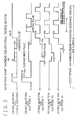
- an erase discharge is performed in the reset period of the next subfield SFn+1 immediately after the sustain discharge (sustain) period of the n-th subfield SFn, as shown in Fig. 4.
- an erase pulse made of a small-width pulse (e.g., a pulse width of 2 ⁇ s or less) is applied to the common electrode X to erase wall charges of each electrode only from the cell which was turned on in the preceding subfield SFn.
- An allowable range (voltage range from the minimum value to the maximum value will be called a driving voltage margin) is defined for the voltage values of various pulses for realizing driving of normally turning an ON cell on based on display data while keeping an OFF cell off. If the discharge starts unexpectedly early owing to nonuniform pixels and temperature condition changes in the small-width erase discharge during the reset period, a necessary wall charge erase fails. In addition, wall charges opposite in polarity to wall charges before an erase may be generated on the common electrode X and scanning electrode Y. This narrows the driving voltage margin.
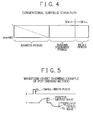
- Fig. 5 shows an example of this driving method.
- Fig. 5 is a driving waveform chart showing part of the reset period in a given subfield.
- positive and negative charges are respectively accumulated in the common electrode X and scanning electrode Y.
- an erase pulse of the voltage Vs made of a small-width pulse is applied to the common electrode X to erase wall charges of the ON cell, as shown in Fig. 5.
- the small-width pulse terminates application of the pulse voltage immediately after a discharge. Most of charge particles generated by the discharge are left in the discharge cell space, attracted by an electrostatic attraction to wall charges of the dielectric layer of the panel, and recombine each other and disappear on the wall surface. Such a strong discharge using a rectangular wave, however, may generate new wall charges opposite in polarity to wall charges before an erase, in the common electrode X and scanning electrode Y, as described above.
- an erase pulse (to be referred to as a positive obtuse wave) which rises to the voltage Vs with a gradual slope and an erase pulse (to be referred to as a negative obtuse wave) which falls to a voltage -Vy with a gradual slope are sequentially applied.
- Wall charges having an inverted polarity which are left owing to an excessive reaction with the small-width pulse, and wall charges which cannot completely be erased by the erase discharge using the small-width pulse are reacted and erased with the potentials of the positive and negative obtuse waves which gradually change with time.
- the amount of wall charges accumulated in a cell which was turned on in the preceding subfield is not always the same in all cells, so the discharge start voltage of each cell varies. If such obtuse waves are applied in this state, discharges sequentially occur from cells in which the pulse voltage during the rise of the positive obtuse wave and the fall of the negative obtuse wave reaches the discharge voltage. Each cell substantially receives the optimum voltage (voltage almost equal to the discharge start voltage). This can erase the residual charges.
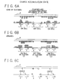
- Figs. 6A to 6C are representations for respectively illustrating the states of charges accumulated in the OFF cell.
- the ON cell accumulates charges enough for satisfactorily starting discharging by the pulse voltage during the rise of the positive obtuse wave and the fall of the negative obtuse wave. By applying these positive and negative obtuse waves, the discharge can occur to erase residual charges. In the OFF cell, however, wall charges accumulated under the influence of the adjacent ON cell are weak. Even if the pulse voltage of the obtuse wave changes to the voltage Vs or -Vy, the OFF cell cannot reach the discharge start voltage, so wall charges cannot be erased and are left.
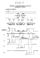
- Fig. 7 is a representation for illustrating this conventional problem.
- a scan pulse of -Vy level is applied to scanning electrodes Yi and Yi+2 of cells C1 and C3 to be turned on in accordance with display data.
- an address pulse of Va level is selectively applied to an address electrode A corresponding to the cells to be turned on, so as to emit light from the cells.
- Embodiments of the present invention aim to overcome the conventional drawbacks, and aim to improve the driving voltage margin in driving a PDP, and reliably to realize driving of normally turning on an ON cell that should be turned on based on display data while keeping an OFF cell off.
- each frame comprises subfields; each of the subfields includes a reset period for performing an erase discharge to make a wall charge distribution in each cell uniform, an address period for generating wall charges in a cell to be turned on in accordance with display data, and a sustain discharge period for discharging the wall charges accumulated in the cell during the address period, to emit light; and the reset period includes first and second erase discharge periods for performing erase discharges for cells having been turned on and not having been turned on, respectively.
- the present invention can apply to a so-called high-contrast driving method.
- erase discharges done separately in the first and second erase discharge periods may be executed in subfields except for a specific subfield.
- the invention also includes a plasma display driving apparatus for driving a plasma display panel in each of the subfields constituting one frame.
- Each of the subfields includes a reset period for performing an erase discharge to make a wall charge distribution in each cell uniform, an address period for generating wall charges in a cell to be turned on in accordance with display data, and a sustain discharge period for discharging the wall charges accumulated in the cell during the address period, to emit light.
- the apparatus comprises control means for performing erase discharges for cells having been turned on and not having been turned on, in first and second erase discharge periods in the reset period, respectively.
- an erase discharge is done in the first erase discharge period for an ON cell turned on in the preceding sustain discharge period, so as to erase wall charges in the ON cell, for example.
- an erase discharge may be done in the second erase discharge period on the basis of a pulse voltage having a different waveform from that for the ON cell. As a result, even weak wall charges accumulated in the OFF cell under the influence of the ON cell can be erased.
- the erase discharge for the OFF cell may be achieved by applying to the first electrode the first erase pulse whose application voltage continuously changes with time in a positive direction, and applying to the second electrode the second erase pulse whose application voltage continuously changes with time in a negative direction. This can widen the potential difference between the first and second electrodes to erase even weak wall charges accumulated in the OFF cell under the influence of the ON cell.
- apparatus may perform erase discharges for ON and OFF cells in the first and second erase discharge periods in the reset period, respectively.
- Weak wall charges that could not completely be erased in the first erase discharge period i.e., weak wall charges accumulated in the OFF cell under the influence of the ON cell can be erased in the second erase discharge period. This makes it possible to prevent an ON operation of the OFF cell that should not be turned on in the subsequent address period and sustain discharge period, and to improve the driving voltage margin.
- the present invention applies to a high-contrast driving method.
- an erase discharge is only done in the reset period without performing any full-surface write discharge.
- Figs. 1 and 2 show the whole arrangement of an AC driving type PDP apparatus and the sectional structure of one cell according to this embodiment, respectively.
- Control means according to the present embodiment comprises a controller 5 in Fig. 1.
- Fig. 8 is a representation of the structure of a subfield for used in explaining a PDP driving method according to this embodiment.
- each subfield is divided into a reset period, an address period, and a sustain discharge (sustain) period.
- the reset period is further divided into the first erase discharge period in which an erase discharge is done for the cell which was turned on in the sustain discharge period of a preceding subfield, and the second erase discharge period in which an erase discharge of wall charges accumulated in an OFF cell under the influence of an adjacent ON cell is done even for the cell which was not turned on in the sustain discharge period of the preceding subfield.
- the residual charges in the ON and OFF cells are respectively erased by different application waveforms.
- a small-width pulse is applied to a common electrode X, and then an erase pulse (to be referred to as the first positive obtuse wave) which gradually rises to a voltage Vs with a gradual slope is applied to a scanning electrode Y.
- Wall charges accumulated in the ON cell by a sustain discharge in the preceding subfield are thereby erased by an erase discharge.
- an erase pulse (corresponding to the first erase pulse in the present invention; to be referred to as the second positive obtuse wave) which gradually rises to a voltage Vax with a gradual slope is applied to the common electrode X (first electrode in the present invention).
- an erase pulse (corresponding to the second erase pulse in the present invention; to be referred to as a negative obtuse wave) which gradually falls to a voltage -Vy with a gradual slope is applied to the scanning electrode Y (second electrode in the present invention).
- Fig. 9 is a waveform chart showing an example of the driving waveform of the AC driving type PDP according to this embodiment, and shows one subfield except for a specific subfield in the high-contrast driving method.
- the scanning electrode Y changes to ground level (0 V).
- a small-width pulse of the voltage Vs (about 180 V) is applied to the common electrode X to erase wall charges in the ON cell.
- the first positive obtuse wave which gradually rises to the voltage Vs with a gradual slope is applied to the scanning electrode Y to erase wall charges having an inverted polarity which are left owing to an excessive reaction with the small-width pulse, and wall charges which cannot completely be erased by the erase discharge using the small-width pulse.
- the negative obtuse wave which gradually falls to the voltage -Vy (about -150 V) with a gradual slope is applied to the scanning electrode Y.
- the second positive obtuse wave, which gradually rises to the voltage Vax with a gradual slope is applied to the common electrode X.
- the residual charges in the OFF cell can be erased before the address period.
- an address pulse is selectively applied to an address electrode A on the basis of display data in the subsequent address period, and a scan pulse is applied to the scanning electrode Y to perform address discharges line-sequentially, any miss discharge on the OFF cell can be prevented.
- the OFF cell which should not be turned on can be prevented from being turned on by the sustain discharge in the OFF cell.
- the application timing of the second positive obtuse wave is the same as the application timing of the negative obtuse wave, for example.
- the pulse widths (rise time and fall time) of the second positive obtuse wave and negative obtuse wave have time widths enough for satisfactorily reaching the ultimate voltages Vax and -Vy at the resistances of circuits for generating these obtuse waves. If the slope of the obtuse wave is steep, the executed erase discharge may become strong. To prevent this, the resistance values of the circuits for generating the second positive obtuse wave and negative obtuse wave are respectively set so as to change these obtuse waves gradually. To allow each obtuse wave to reach a necessary voltage even at such resistances, the rise/fall time is set to, e.g., 100 ⁇ sec or more.
- the final ultimate voltage Vax of the second positive obtuse wave is set such that the potential difference from the ultimate voltage -Vy of the negative obtuse wave is around the discharge start voltage (voltage at which a discharge occurs regardless of the presence/absence of wall charges) between the electrodes X and Y and is lower than this discharge start voltage. This is because a full discharge occurs if the voltage difference between the electrodes X and Y is equal to or larger than the discharge start voltage.
- Fig. 11 shows an example of an arrangement for attaining the purpose.
- Fig. 11 shows part of the AC driving type PDP apparatus shown in Fig. 1, and shows voltage setting means of this embodiment.
- a positive obtuse wave generator 21 is for generating the second positive obtuse wave.
- a negative obtuse wave generator 22 is for generating the negative obtuse wave.
- the positive and negative obtuse wave generators 21 and 22 are respectively incorporated in the X driver 2 and Y driver 3 shown in Fig. 1.
- the positive and negative obtuse wave generators 21 and 22 are connected to the common electrode X and scanning electrode Y of the AC driving type PDP 1, respectively.
- the positive obtuse wave generator 21 comprises a resistor 23 for determining the rise slope of the second positive obtuse wave.
- the negative obtuse wave generator 22 comprises a resistor 24 for determining the fall slope of the negative obtuse wave.
- the resistor 23 for the second positive obtuse wave is variable so as to increase/decrease a resistance value Rx and increase/decrease the value of the ultimate voltage Vax of the second positive obtuse wave.
- the resistor 24 in the negative obtuse wave generator 22 may also be variable so as to increase/decrease a resistance value Ry.
- the negative obtuse wave and second positive obtuse wave have the same application start timing, whereas the resistance values Rx and Ry cannot take the same value because of different final ultimate voltages. If the second positive obtuse wave rises too steeply, residual charges excessively react; if the second positive obtuse wave rises too slowly, the wave does not reach a desired voltage. Considering them, the resistance value Rx for the second positive obtuse wave must be optimized.
- Figs. 12A to 12D are representations for illustrating the respective states of wall charges accumulated in the address electrode A, common electrode X, and scanning electrode Y when the PDP driving method according to this embodiment is applied.
- the charge accumulation states shown in Figs. 12A to 12C correspond to the states shown in Figs. 6A to 6C, respectively. That is, wall charges accumulated in the ON cell at the end of the sustain discharge period are erased by applying the small-width pulse and first positive obtuse wave in the first erase discharge period, and applying the negative obtuse wave in the second erase discharge period.
- the second positive obtuse wave is applied in synchronism with application of the negative obtuse wave in the second erase discharge period, so as to erase even weak residual charges accumulated in the OFF cell under the influence of the ON cell, as shown in Fig. 12D.
- This can prevent an ON operation of the OFF cell that should not be turned on in the subsequent address period and sustain discharge period, and can improve the driving voltage margin.
- an obtuse wave whose change rate per unit time gradually changes is applied as an erase pulse whose application voltage gradually changes with time, to the common electrode X and scanning electrode Y in the reset period.
- the present invention is not limited to this.
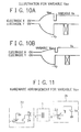
- a triangular wave whose application voltage gradually changes at a constant change rate per unit time may be applied, as shown in Fig. 13.
- the rise start timing of the second positive obtuse wave and the fall start timing of the negative obtuse wave are synchronized.
- the present invention is not limited to this.
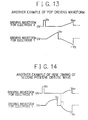
- the rise start timing of the second positive obtuse wave applied to the common electrode X may be delayed from the fall start timing of the negative obtuse wave applied to the scanning electrode Y, so as to narrow the pulse width of the second positive obtuse wave, as shown in Fig. 14.
- the positive obtuse wave that rises in a positive direction is applied as an obtuse wave applied to the common electrode X in synchronism with the negative obtuse wave to the scanning electrode Y.
- a negative obtuse wave that falls in a negative direction may be applied to the common electrode X in synchronism with the first positive obtuse wave to the scanning electrode Y.
- the alternative method can be taken only when a time margin (e.g., an interval of 10 ⁇ sec or more) is set between the fall of the small-width pulse and application of the negative obtuse wave. This is because an erase may undesirably be done in an unstable charge state if the interval between the small-width pulse and negative obtuse wave is less than 10 ⁇ sec.
- This embodiment has exemplified the high-contrast driving method. That is, a full-surface write and full-surface erase are performed during the reset period in the first subfield of each frame, and the above-described driving method is executed in the second and subsequent subfields. But, the principle of this embodiment is not limited to the high-contrast driving method.
- the same driving method as in this embodiment can apply to each of the subfields to produce the same effects as in the embodiment. Even when small-width erase discharges are done in the reset periods of all subfields without performing full-surface write discharges, the present invention is effective.
Landscapes
- Engineering & Computer Science (AREA)
- Physics & Mathematics (AREA)
- Computer Hardware Design (AREA)
- General Physics & Mathematics (AREA)
- Theoretical Computer Science (AREA)
- Power Engineering (AREA)
- Plasma & Fusion (AREA)
- Control Of Gas Discharge Display Tubes (AREA)
- Control Of Indicators Other Than Cathode Ray Tubes (AREA)
- Transforming Electric Information Into Light Information (AREA)
- Devices For Indicating Variable Information By Combining Individual Elements (AREA)
Applications Claiming Priority (2)
| Application Number | Priority Date | Filing Date | Title |
|---|---|---|---|
| JP11377399 | 1999-04-21 | ||
| JP11377399A JP4124305B2 (ja) | 1999-04-21 | 1999-04-21 | プラズマディスプレイの駆動方法および駆動装置 |
Publications (2)
| Publication Number | Publication Date |
|---|---|
| EP1047042A2 true EP1047042A2 (fr) | 2000-10-25 |
| EP1047042A3 EP1047042A3 (fr) | 2002-08-21 |
Family
ID=14620768
Family Applications (1)
| Application Number | Title | Priority Date | Filing Date |
|---|---|---|---|
| EP99309449A Withdrawn EP1047042A3 (fr) | 1999-04-21 | 1999-11-26 | Appareil d'affichage à plasma et méthode de commande d'un tel appareil |
Country Status (6)
| Country | Link |
|---|---|
| US (1) | US6836261B1 (fr) |
| EP (1) | EP1047042A3 (fr) |
| JP (1) | JP4124305B2 (fr) |
| KR (2) | KR100638151B1 (fr) |
| CN (1) | CN1192343C (fr) |
| TW (1) | TW561444B (fr) |
Cited By (6)
| Publication number | Priority date | Publication date | Assignee | Title |
|---|---|---|---|---|
| EP1288896A3 (fr) * | 2001-08-08 | 2005-08-24 | Fujitsu Hitachi Plasma Display Limited | Méthode de commande d'un panneau d'affichage à plasma |
| EP1598801A1 (fr) | 2004-05-21 | 2005-11-23 | Samsung SDI Co., Ltd. | Procédé de commande d'écran à plasma, et écran à plasma |
| DE10260612B4 (de) * | 2002-03-30 | 2007-04-12 | Samsung Electronics Co., Ltd., Suwon | Vorrichtung und Verfahren für das automatische Einstellen einer Rücksetzrampenwellenform eines Plasmaanzeigefeldes |
| EP1758076A4 (fr) * | 2004-05-25 | 2007-10-31 | Shinoda Plasma Corp | Procede pour entrainer le dispositif d'affichage de decharge de gaz |
| EP1324301A3 (fr) * | 2001-11-14 | 2009-04-08 | Samsung SDI Co. Ltd. | Procédé et appareil de commande d'un panneau d'affichage à plasma |
| EP1768092A3 (fr) * | 2005-09-26 | 2009-10-14 | LG Electronics Inc. | Appareil d'affichage à plasma et son procédé de commande |
Families Citing this family (30)
| Publication number | Priority date | Publication date | Assignee | Title |
|---|---|---|---|---|
| JP3424587B2 (ja) * | 1998-06-18 | 2003-07-07 | 富士通株式会社 | プラズマディスプレイパネルの駆動方法 |
| JP2002162931A (ja) * | 2000-11-24 | 2002-06-07 | Nec Corp | プラズマディスプレイパネルの駆動方法 |
| JP4656742B2 (ja) * | 2001-02-27 | 2011-03-23 | パナソニック株式会社 | プラズマディスプレイパネルの駆動方法 |
| JP2002328648A (ja) * | 2001-04-26 | 2002-11-15 | Nec Corp | Ac型プラズマディスプレイパネルの駆動方法および駆動装置 |
| KR100385882B1 (ko) * | 2001-05-28 | 2003-06-02 | 엘지전자 주식회사 | 플라즈마 디스플레이 패널의 소거방전 구동방법 및 그의구동장치 |
| US6867754B2 (en) * | 2001-06-04 | 2005-03-15 | Samsung Sdi Co., Ltd. | Method for resetting plasma display panel for improving contrast |
| JP2003005701A (ja) * | 2001-06-20 | 2003-01-08 | Pioneer Electronic Corp | プラズマディスプレイパネルの駆動方法 |
| KR100433212B1 (ko) * | 2001-08-21 | 2004-05-28 | 엘지전자 주식회사 | 어드레스 소비전력 저감을 위한 플라즈마 디스플레이패널의 구동방법 및 장치 |
| TWI239026B (en) * | 2001-08-29 | 2005-09-01 | Au Optronics Corp | Plasma display panel structure and its driving method |
| KR100493912B1 (ko) * | 2001-11-24 | 2005-06-10 | 엘지전자 주식회사 | 플라즈마 디스플레이 패널의 구동장치 및 방법 |
| KR100458569B1 (ko) * | 2002-02-15 | 2004-12-03 | 삼성에스디아이 주식회사 | 플라즈마 디스플레이 패널의 구동방법 |
| JP4170713B2 (ja) * | 2002-09-13 | 2008-10-22 | パイオニア株式会社 | 表示パネルの駆動方法 |
| KR100490620B1 (ko) * | 2002-11-28 | 2005-05-17 | 삼성에스디아이 주식회사 | 플라즈마 디스플레이 패널의 구동 방법 |
| KR100489276B1 (ko) * | 2003-01-16 | 2005-05-17 | 엘지전자 주식회사 | 플라즈마 디스플레이 패널의 구동방법 |
| JP4321675B2 (ja) * | 2003-03-31 | 2009-08-26 | 株式会社日立プラズマパテントライセンシング | プラズマディスプレイパネルの駆動方法 |
| EP1471491A3 (fr) * | 2003-04-22 | 2005-03-23 | Samsung SDI Co., Ltd. | Panneau d'affichage à plasma et son procédé de commande |
| KR100515341B1 (ko) * | 2003-09-02 | 2005-09-15 | 삼성에스디아이 주식회사 | 플라즈마 디스플레이 패널의 구동 장치 |
| KR100570611B1 (ko) * | 2003-10-29 | 2006-04-12 | 삼성에스디아이 주식회사 | 플라즈마 디스플레이 패널과 그의 구동방법 |
| JP2005257880A (ja) * | 2004-03-10 | 2005-09-22 | Pioneer Electronic Corp | 表示パネルの駆動方法 |
| JP4576139B2 (ja) * | 2004-03-22 | 2010-11-04 | パナソニック株式会社 | 表示パネルの駆動方法 |
| JP2005301053A (ja) * | 2004-04-14 | 2005-10-27 | Pioneer Electronic Corp | プラズマディスプレイパネルの駆動方法、駆動回路及び駆動プログラム |
| CN100369083C (zh) * | 2004-10-10 | 2008-02-13 | 东南大学 | 槽型等离子体显示板行电极的驱动电路及其驱动方法 |
| CN100369084C (zh) * | 2004-10-14 | 2008-02-13 | 东南大学 | 槽型等离子体显示板的高电压扫描维持驱动电路及其驱动方法 |
| KR100739052B1 (ko) * | 2005-06-03 | 2007-07-12 | 삼성에스디아이 주식회사 | 플라즈마 표시 장치 및 그 구동 방법 |
| JPWO2007088601A1 (ja) * | 2006-02-01 | 2009-06-25 | 日立プラズマディスプレイ株式会社 | プラズマディスプレイパネルの駆動方法およびプラズマディスプレイ装置 |
| JP4902601B2 (ja) * | 2008-07-08 | 2012-03-21 | 日立プラズマディスプレイ株式会社 | プラズマディスプレイ装置の駆動方法 |
| JP4902724B2 (ja) * | 2009-11-19 | 2012-03-21 | 日立プラズマディスプレイ株式会社 | プラズマディスプレイ装置の駆動方法 |
| JP4902766B2 (ja) * | 2010-04-19 | 2012-03-21 | 日立プラズマディスプレイ株式会社 | プラズマディスプレイ装置の駆動方法 |
| JP4657376B2 (ja) * | 2010-07-29 | 2011-03-23 | パナソニック株式会社 | プラズマディスプレイパネルの駆動方法 |
| JP5099238B2 (ja) * | 2011-02-14 | 2012-12-19 | 株式会社日立製作所 | プラズマディスプレイ装置 |
Family Cites Families (11)
| Publication number | Priority date | Publication date | Assignee | Title |
|---|---|---|---|---|
| JP2756053B2 (ja) | 1992-05-11 | 1998-05-25 | 富士通株式会社 | 交流駆動型プラズマディスプレイパネル駆動方法 |
| JP3370405B2 (ja) | 1993-12-17 | 2003-01-27 | 富士通株式会社 | 平面表示装置及びその駆動方法 |
| US5745086A (en) * | 1995-11-29 | 1998-04-28 | Plasmaco Inc. | Plasma panel exhibiting enhanced contrast |
| JP3433032B2 (ja) | 1995-12-28 | 2003-08-04 | パイオニア株式会社 | 面放電交流型プラズマディスプレイ装置及びその駆動方法 |
| JP3704813B2 (ja) * | 1996-06-18 | 2005-10-12 | 三菱電機株式会社 | プラズマディスプレイパネルの駆動方法及びプラズマディスプレイ |
| JP3348610B2 (ja) * | 1996-11-12 | 2002-11-20 | 富士通株式会社 | プラズマディスプレイパネルの駆動方法及び装置 |
| JP3517551B2 (ja) * | 1997-04-16 | 2004-04-12 | パイオニア株式会社 | 面放電型プラズマディスプレイパネルの駆動方法 |
| JP3573968B2 (ja) * | 1997-07-15 | 2004-10-06 | 富士通株式会社 | プラズマディスプレイの駆動方法及び駆動装置 |
| JP3582964B2 (ja) * | 1997-08-29 | 2004-10-27 | パイオニア株式会社 | プラズマディスプレイパネルの駆動装置 |
| JPH11209040A (ja) * | 1998-01-20 | 1999-08-03 | Mitsubishi Electric Corp | エレベーター装置 |
| TW451182B (en) | 1998-11-20 | 2001-08-21 | Acer Media Technology Inc | Driving method of image to improve the dynamic image profile of display |
-
1999
- 1999-04-21 JP JP11377399A patent/JP4124305B2/ja not_active Expired - Fee Related
- 1999-10-23 KR KR1019990046179A patent/KR100638151B1/ko not_active Expired - Fee Related
- 1999-11-16 US US09/440,704 patent/US6836261B1/en not_active Expired - Fee Related
- 1999-11-19 TW TW088120225A patent/TW561444B/zh not_active IP Right Cessation
- 1999-11-26 EP EP99309449A patent/EP1047042A3/fr not_active Withdrawn
- 1999-12-22 CN CNB991265114A patent/CN1192343C/zh not_active Expired - Fee Related
-
2006
- 2006-06-29 KR KR1020060059443A patent/KR100658481B1/ko not_active Expired - Fee Related
Cited By (12)
| Publication number | Priority date | Publication date | Assignee | Title |
|---|---|---|---|---|
| EP1288896A3 (fr) * | 2001-08-08 | 2005-08-24 | Fujitsu Hitachi Plasma Display Limited | Méthode de commande d'un panneau d'affichage à plasma |
| US7212177B2 (en) | 2001-08-08 | 2007-05-01 | Fujitsu Hitachi Plasma Display Limited | Method of driving a plasma display apparatus |
| EP1515296A3 (fr) * | 2001-08-08 | 2007-05-02 | Fujitsu Hitachi Plasma Display Limited | Méthode de commande d'un panneau d'affichage à plasma |
| EP1873743A3 (fr) * | 2001-08-08 | 2008-07-16 | Fujitsu Hitachi Plasma Display Limited | Méthode de commande d'un panneau d'affichage à plasma |
| US7868852B2 (en) | 2001-08-08 | 2011-01-11 | Fujitsu Hitachi Plasma Display Ltd. | Method of driving a plasma display apparatus to suppress background light emission |
| US8094092B2 (en) | 2001-08-08 | 2012-01-10 | Fujitsu Hitachi Plasma Display Limited | Plasma display apparatus and a method of driving the plasma display apparatus |
| US8797237B2 (en) | 2001-08-08 | 2014-08-05 | Hitachi Maxell, Ltd. | Plasma display apparatus and method of driving the plasma display apparatus |
| EP1324301A3 (fr) * | 2001-11-14 | 2009-04-08 | Samsung SDI Co. Ltd. | Procédé et appareil de commande d'un panneau d'affichage à plasma |
| DE10260612B4 (de) * | 2002-03-30 | 2007-04-12 | Samsung Electronics Co., Ltd., Suwon | Vorrichtung und Verfahren für das automatische Einstellen einer Rücksetzrampenwellenform eines Plasmaanzeigefeldes |
| EP1598801A1 (fr) | 2004-05-21 | 2005-11-23 | Samsung SDI Co., Ltd. | Procédé de commande d'écran à plasma, et écran à plasma |
| EP1758076A4 (fr) * | 2004-05-25 | 2007-10-31 | Shinoda Plasma Corp | Procede pour entrainer le dispositif d'affichage de decharge de gaz |
| EP1768092A3 (fr) * | 2005-09-26 | 2009-10-14 | LG Electronics Inc. | Appareil d'affichage à plasma et son procédé de commande |
Also Published As
| Publication number | Publication date |
|---|---|
| US6836261B1 (en) | 2004-12-28 |
| JP2000305519A (ja) | 2000-11-02 |
| KR20000067792A (ko) | 2000-11-25 |
| KR100638151B1 (ko) | 2006-10-26 |
| EP1047042A3 (fr) | 2002-08-21 |
| KR20060088087A (ko) | 2006-08-03 |
| CN1192343C (zh) | 2005-03-09 |
| KR100658481B1 (ko) | 2006-12-19 |
| JP4124305B2 (ja) | 2008-07-23 |
| CN1271156A (zh) | 2000-10-25 |
| TW561444B (en) | 2003-11-11 |
Similar Documents
| Publication | Publication Date | Title |
|---|---|---|
| US6836261B1 (en) | Plasma display driving method and apparatus | |
| US6512501B1 (en) | Method and device for driving plasma display | |
| US8179342B2 (en) | Method and apparatus for driving plasma display panel | |
| KR100711034B1 (ko) | 플라즈마 표시 장치 및 그 구동 방법 | |
| EP1585096A2 (fr) | Dispositif d'affichage d'image par plasma et son procédé de commande | |
| KR20040094225A (ko) | 플라즈마 디스플레이 패널의 구동방법 및 장치 | |
| JP4205865B2 (ja) | Ac型プラズマディスプレイ装置 | |
| US7583241B2 (en) | Plasma display apparatus and driving method of the same | |
| US20060262041A1 (en) | Apparatus and method for operating plasma display panel | |
| WO2006112233A1 (fr) | Panneau d’affichage a plasma et son procede d’attaque | |
| US7006060B2 (en) | Plasma display panel and method of driving the same capable of providing high definition and high aperture ratio | |
| US7911421B2 (en) | Driving device and method for plasma display panel | |
| US20050212723A1 (en) | Driving method of plasma display panel and plasma display device | |
| US7642992B2 (en) | Plasma display apparatus and driving method thereof | |
| US20060007062A1 (en) | Plasma display panel and driving method and apparatus thereof | |
| US20060109212A1 (en) | Plasma display device and method for driving the same | |
| US7408532B2 (en) | Plasma display device and drive method for use in plasma display device | |
| US20070013616A1 (en) | Plasma display apparatus and driving method thereof | |
| JP4130460B2 (ja) | プラズマディスプレイの駆動方法および駆動装置 | |
| US20070069986A1 (en) | Plasma display apparatus and driving method thereof | |
| EP1775697A2 (fr) | Appareil d'affichage à plasma | |
| US20070008248A1 (en) | Plasma display apparatus and driving method thereof | |
| KR20050040558A (ko) | 플라즈마 디스플레이 패널의 구동 방법 및 플라즈마 표시장치 |
Legal Events
| Date | Code | Title | Description |
|---|---|---|---|
| PUAI | Public reference made under article 153(3) epc to a published international application that has entered the european phase |
Free format text: ORIGINAL CODE: 0009012 |
|
| AK | Designated contracting states |
Kind code of ref document: A2 Designated state(s): AT BE CH CY DE DK ES FI FR GB GR IE IT LI LU MC NL PT SE |
|
| AX | Request for extension of the european patent |
Free format text: AL;LT;LV;MK;RO;SI |
|
| PUAL | Search report despatched |
Free format text: ORIGINAL CODE: 0009013 |
|
| AK | Designated contracting states |
Kind code of ref document: A3 Designated state(s): AT BE CH CY DE DK ES FI FR GB GR IE IT LI LU MC NL PT SE |
|
| AX | Request for extension of the european patent |
Free format text: AL;LT;LV;MK;RO;SI |
|
| 17P | Request for examination filed |
Effective date: 20021113 |
|
| AKX | Designation fees paid |
Designated state(s): DE FR GB |
|
| RAP1 | Party data changed (applicant data changed or rights of an application transferred) |
Owner name: HITACHI, LTD. |
|
| RAP1 | Party data changed (applicant data changed or rights of an application transferred) |
Owner name: HITACHI PLASMA PATENT LICENSING CO., LTD. |
|
| GRAP | Despatch of communication of intention to grant a patent |
Free format text: ORIGINAL CODE: EPIDOSNIGR1 |
|
| STAA | Information on the status of an ep patent application or granted ep patent |
Free format text: STATUS: THE APPLICATION IS DEEMED TO BE WITHDRAWN |
|
| 18D | Application deemed to be withdrawn |
Effective date: 20101203 |